EP1050951A2 - Schaltungsanordnung für eine getaktete Stromversorgung - Google Patents
Schaltungsanordnung für eine getaktete Stromversorgung Download PDFInfo
- Publication number
- EP1050951A2 EP1050951A2 EP00108178A EP00108178A EP1050951A2 EP 1050951 A2 EP1050951 A2 EP 1050951A2 EP 00108178 A EP00108178 A EP 00108178A EP 00108178 A EP00108178 A EP 00108178A EP 1050951 A2 EP1050951 A2 EP 1050951A2
- Authority
- EP
- European Patent Office
- Prior art keywords
- semiconductor switch
- power supply
- circuit arrangement
- clocked power
- supply according
- Prior art date
- Legal status (The legal status is an assumption and is not a legal conclusion. Google has not performed a legal analysis and makes no representation as to the accuracy of the status listed.)
- Granted
Links
Images


Classifications
-
- H—ELECTRICITY
- H02—GENERATION; CONVERSION OR DISTRIBUTION OF ELECTRIC POWER
- H02M—APPARATUS FOR CONVERSION BETWEEN AC AND AC, BETWEEN AC AND DC, OR BETWEEN DC AND DC, AND FOR USE WITH MAINS OR SIMILAR POWER SUPPLY SYSTEMS; CONVERSION OF DC OR AC INPUT POWER INTO SURGE OUTPUT POWER; CONTROL OR REGULATION THEREOF
- H02M3/00—Conversion of DC power input into DC power output
- H02M3/02—Conversion of DC power input into DC power output without intermediate conversion into AC
- H02M3/04—Conversion of DC power input into DC power output without intermediate conversion into AC by static converters
- H02M3/10—Conversion of DC power input into DC power output without intermediate conversion into AC by static converters using discharge tubes with control electrode or semiconductor devices with control electrode
- H02M3/145—Conversion of DC power input into DC power output without intermediate conversion into AC by static converters using discharge tubes with control electrode or semiconductor devices with control electrode using devices of a triode or transistor type requiring continuous application of a control signal
- H02M3/155—Conversion of DC power input into DC power output without intermediate conversion into AC by static converters using discharge tubes with control electrode or semiconductor devices with control electrode using devices of a triode or transistor type requiring continuous application of a control signal using semiconductor devices only
- H02M3/156—Conversion of DC power input into DC power output without intermediate conversion into AC by static converters using discharge tubes with control electrode or semiconductor devices with control electrode using devices of a triode or transistor type requiring continuous application of a control signal using semiconductor devices only with automatic control of output voltage or current, e.g. switching regulators
- H02M3/158—Conversion of DC power input into DC power output without intermediate conversion into AC by static converters using discharge tubes with control electrode or semiconductor devices with control electrode using devices of a triode or transistor type requiring continuous application of a control signal using semiconductor devices only with automatic control of output voltage or current, e.g. switching regulators including plural semiconductor devices as final control devices for a single load
-
- H—ELECTRICITY
- H02—GENERATION; CONVERSION OR DISTRIBUTION OF ELECTRIC POWER
- H02M—APPARATUS FOR CONVERSION BETWEEN AC AND AC, BETWEEN AC AND DC, OR BETWEEN DC AND DC, AND FOR USE WITH MAINS OR SIMILAR POWER SUPPLY SYSTEMS; CONVERSION OF DC OR AC INPUT POWER INTO SURGE OUTPUT POWER; CONTROL OR REGULATION THEREOF
- H02M1/00—Details of apparatus for conversion
- H02M1/0048—Circuits or arrangements for reducing losses
-
- H—ELECTRICITY
- H02—GENERATION; CONVERSION OR DISTRIBUTION OF ELECTRIC POWER
- H02M—APPARATUS FOR CONVERSION BETWEEN AC AND AC, BETWEEN AC AND DC, OR BETWEEN DC AND DC, AND FOR USE WITH MAINS OR SIMILAR POWER SUPPLY SYSTEMS; CONVERSION OF DC OR AC INPUT POWER INTO SURGE OUTPUT POWER; CONTROL OR REGULATION THEREOF
- H02M1/00—Details of apparatus for conversion
- H02M1/44—Circuits or arrangements for compensating for electromagnetic interference in converters or inverters
-
- Y—GENERAL TAGGING OF NEW TECHNOLOGICAL DEVELOPMENTS; GENERAL TAGGING OF CROSS-SECTIONAL TECHNOLOGIES SPANNING OVER SEVERAL SECTIONS OF THE IPC; TECHNICAL SUBJECTS COVERED BY FORMER USPC CROSS-REFERENCE ART COLLECTIONS [XRACs] AND DIGESTS
- Y02—TECHNOLOGIES OR APPLICATIONS FOR MITIGATION OR ADAPTATION AGAINST CLIMATE CHANGE
- Y02B—CLIMATE CHANGE MITIGATION TECHNOLOGIES RELATED TO BUILDINGS, e.g. HOUSING, HOUSE APPLIANCES OR RELATED END-USER APPLICATIONS
- Y02B70/00—Technologies for an efficient end-user side electric power management and consumption
- Y02B70/10—Technologies improving the efficiency by using switched-mode power supplies [SMPS], i.e. efficient power electronics conversion e.g. power factor correction or reduction of losses in power supplies or efficient standby modes
Definitions
- the invention relates to a circuit arrangement for a clocked Power supply with an integrated circuit, the one with a first and a second supply potential connection is connected and the one switching device, a control circuit controlling the switching device and has a diode.
- a coil is also provided with the switching device and a first output terminal connected is. Between the first and a second output terminal is a load interconnect that is a charge storage is connected in parallel.
- Step-down converters also called step-down regulators, are used mainly used where there is a high degree of efficiency generates a lower one from a high supply voltage shall be.
- a high degree of efficiency is particularly important for battery-operated ones Devices.
- the heating of the electronic stands for high efficiency Components due to power loss in the foreground. This is especially in applications of automotive electronics Case.
- clocked power supplies are in automotive electronics due to electromagnetic Compatibility has not been used so far. Instead, were used to generate a regulated supply voltage Linear controller used, which, however, in Warm up operation.
- Linear controllers are common in automotive electronics operated with a nominal current of 400 mA. On a lateral one The difference between the input and bipolar transistor drops the output voltage. The product of the differential voltage and the nominal current is converted into heat loss. The greater the voltage difference between the input and the Output of the bipolar transistor is, the higher the Losses.
- the use of a linear regulator in a 42 volt electrical system are due to the rapidly increasing power loss therefore unsuitable. The use of a switching regulator for load currents around 1 A is therefore desirable.
- EMC electromagnetic compatibility
- the object of the present invention is therefore to a circuit arrangement for a clocked power supply to provide, on the one hand, the requirements for electromagnetic Compatibility fulfilled and on the other hand only one low power dissipation.
- This task is accomplished with a circuit arrangement according to the Features of claim 1 fulfilled, wherein the switching device a first and a second semiconductor switch having. This makes it possible, even at high clock frequencies to produce slow switching edges, which causes the heating the semiconductor switch remains low.
- An essential finding of the invention is that the electromagnetic radiation mainly through short Current rise times of switching operations is caused during steep voltage increases with constant current for the electromagnetic compatibility of rather minor Meaning. Generate common clocked power supplies but slow voltage edges and fast current transitions, which means that the EMC requirement cannot be met. The generation of a slow current transition and one comparatively fast voltage edge is with the Switching device allows a first and a has second semiconductor switch.
- the first and second semiconductor switches are advantageously with their load routes in parallel and are each controlled separately from the control.
- the Semiconductor switches are advantageously designed in such a way that that with the same threshold voltage, the first semiconductor switch a larger one compared to the second semiconductor switch Can carry electricity.
- the first semiconductor switch thus has a low on resistance on that in conjunction with its gate-drain capacitance a sufficiently high slope of the voltage edges guaranteed.
- the second semiconductor switch is dimensioned so that its drain saturation current is just sufficient, to take over the entire load current.
- To switch on becomes the gate-source voltage with a defined edge steepness slowly from a value below the threshold voltage increased to its maximum value.
- To switch off the Gate-source voltage with a comparable slope diminished again.
- the desired, slow slope of the current can be at the second semiconductor switch, which has a small area and thus a small input capacity has, very easy to adjust.
- the required small current rise rate results and therefore a low level of EMC radiation.
- the two semiconductor switches are advantageously activated such that the second semiconductor switch before the first semiconductor switch is turned on. Farther it is advantageous if the second semiconductor switch after the first semiconductor switch is turned off. this has as a result that the load current essentially always over a single semiconductor switch flows. For a short time only the switching processes find a distribution of the load current instead, which the current rise - depending on the time transition of the current from the first to the second semiconductor switch - enlarge shortly before reaching the nominal current can. At this point, however, the EMC emission is no longer critical.
- Load path of the first semiconductor switch a series connection from a first resistance and the load path of the second semiconductor switch connected in parallel.
- the first Resistance is preferably designed as a discrete component.
- the first resistor can be dimensioned that at nominal voltage at the first supply potential connection and at maximum load current through the second semiconductor switch the nominal voltage drops. This is how the heat loss is generated for the most part in the resistance that is outside of the integrated circuit. A strong warming the integrated circuit is thus prevented.
- the first resistance during switching operations can be done with linear rise and no waiting time between switching operations of the first and the second semiconductor switch approx. 75% of switching losses. As a result, only 25% of the heat loss from the integrated circuit must be dealt with.
- the heat loss share of the resistance can be enlarged even further if there is a wait between the switching operations of the first and second semiconductor switches is provided.
- the advantage of this design is that in the simplest and very inexpensive Way the power dissipation in the integrated circuit can be kept low.
- a second resistor is also included connected to the diode and the first output terminal.
- the second Charge storage is preferably designed as a discrete component, while the second resistor and the second diode in the integrated circuit can be provided. This Design is particularly advantageous if the Voltage rise, d. H. the switching process of the first semiconductor switch is chosen much faster than the current rise, caused by the second semiconductor switch is. Furthermore, there is the advantage that the total resulting heat loss is very low.
- the control advantageously has a clock, one Pulse width modulator and a driver arrangement for the Switching device on.
- FIG. 1 shows a first embodiment of the invention Circuit arrangement for a clocked power supply.
- the circuit arrangement according to the invention has one integrated circuit IC on with a first supply potential connection 1 and a second supply potential connection 2 is connected. Furthermore, in the integrated Circuit IC provided a drive circuit AS, the one Control device SV controls.
- the switching device SV is on the input side with the first supply potential connection 1 connected.
- the switching device SV is on the output side a coil is connected to a first output terminal A1. Between the first output terminal A1 and a second output terminal A load Z is provided for A2.
- the load Z is a first charge storage C1 connected in parallel.
- the coil L, the first charge storage C1 and the load Z are outside of the integrated circuit IC.
- the first output terminal A1 is connected via a feedback branch RS to the control circuit AS connected.
- the control circuit AS has a clock 3, a pulse width modulator 4 and one Driver arrangement 5.
- the driver arrangement 5 generates a first control signal AS1 and a second control signal AS2, each a first semiconductor switch T1 and a second semiconductor switch T2 supplied to the control device SV become.
- the first and the second semiconductor switch T1, T2 is designed as a MOSFET, however, bipolar transistors could also be used instead or any other controllable switch can be used.
- the MOSFETs T1, T2 are parallel with their drain-source paths switched, the Dram connections each with the first supply potential connection are connected.
- the supply voltage is connected to the operating voltage, while at the second supply potential connection a reference potential, e.g. B. mass.
- the source connections of the MOSFETs T1, T2 are connected to the first terminal of the coil L.
- the MOSFETs T1, T2 are dimensioned so that the same Threshold voltage, d. H. Gate-source voltage the first MOSFET T1 can carry a high current while the second MOSFET T2 carries a much lower current. this means nothing other than that of the MOSFET T1 an essential has a larger number of MOS cells than the MOSFET T2.
- a first diode D1 is provided, wherein the anode connection with the second supply potential connection 2 communicates.
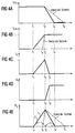
- FIG. 4a shows the drain-source voltage of the semiconductor switches T1 and T2, while FIG. 4b shows the associated total current I Ges .
- the dashed lines represent the switching behavior of an arrangement according to the prior art.
- a semiconductor switch is switched on according to the prior art.
- the total current I Ges has risen to its nominal current. The rate of current rise is relatively steep. From time t 2 , the current remains at its nominal current I N.
- the drain-source voltage U ds drops until time t b .
- the associated power loss is shown in broken lines in FIG. 4e.
- the power loss is represented by the area shown under the dashed line.
- the current rise rate ie the time difference between switching on and reaching the nominal current (t 2 - t 1 ) must be increased compared to the prior art (t 2 - t a ).
- the flat current rise is achieved by means of the second MOSFET t 2 , as shown in FIG. 4c.
- the gate-source voltage of the second MOSFET T 2 is increased with a defined edge steepness, as shown in FIG. 4c, from a value below the threshold voltage up to its maximum value.
- the lower edge steepness can be easily set in a MOSFET with a small area and small input capacitance.
- FIG 2 shows a second embodiment of the invention Circuit arrangement. Compared to the embodiment This preferred embodiment differs from FIG only in that between the drain connection of the second MOSFETs T2 and the first supply potential connection 1 a first resistor R1 is connected. This means nothing but that of the drain-source load path of the first MOSFET T1 the series circuit from a first Resistor R1 and the drain-source path of the second MOSFET T2 is connected in parallel.
- the first resistor R1 is located itself outside of the integrated circuit IC. Through this arrangement, a large part of the accruing Power loss implemented in the first resistor R1 be so that for in the integrated circuit IC converted power loss of the dash-dotted line in Figure 4e Set course 2.
- the power loss area is consequently only represented by two paraboloid surfaces.
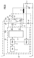
- FIG. 3 shows a third preferred embodiment the circuit arrangement according to the invention.
- the first resistance R1 from FIG. 2 is made up of a series circuit second charge storage C2 and a second diode D2 replaced.
- the cathode of the second diode D2 is with the Drain connection of the second semiconductor switch T2 connected, during the anode connection with the second charge store C2 connected is.
- the connection point between the charge storage C2 and the second diode D2 is connected to the first terminal a resistor R2 connected, the other connection with the first output terminal A1 is connected.
- the second charge store C2 is advantageously outside the integrated Circuit IC arranged while the second resistor R2 and the second diode D2 on the integrated Circuit IC can be integrated.
- the second charge store C2 is on the differential voltage between the first supply potential connection 1 and the first output terminal A1 is charged.
- the first off Semiconductor switch falls on the drain-source path of the second semiconductor switch T2 approximately at the output terminal AK1 applied voltage, i. H. the resulting power loss is very small.
- the Current of the coil L slowly via the first diode D1 to the first Charge storage C1. If the first semiconductor switch T1 is switched on or off, the current goes off very quickly second semiconductor switch T2 to the first semiconductor switch T1 over (or vice versa).
- connection has the advantage that a maximum of one external Component (charge storage C2) required. As a consequence, that of the integrated circuit and the external charge storage C2 area kept very small can be. Furthermore, the electromagnetic radiation in the third embodiment reduced to an absolute minimum.
- the third example is in particular advantageous if the voltage increase, i.e. H. the switching process of the first semiconductor switch selected much faster is called the current rise by the second semiconductor switch is conditional. The resulting heat loss again significantly reduced.
Landscapes
- Engineering & Computer Science (AREA)
- Power Engineering (AREA)
- Dc-Dc Converters (AREA)
Abstract
Description
- Figur 1
- ein erstes Ausführungsbeispiel der erfindungsgemäßen Schaltungsanordnung,
- Figur 2
- ein zweites Ausführungsbeispiel der erfindungsgemäßen Anordnung,
- Figur 3
- ein drittes Ausführungsbeispiel der erfindungsgemäßen Schaltungsanordnung und
- Figur 4
- die zeitlichen Spannungs-/Strom-Verläufe an den Halbleiterschaltern sowie die entstehende Verlustleistung.
- 1
- erste Versorgungspotentialanschluß
- 2
- zweiter Versorgungspotentialanschluß
- 3
- Taktgeber
- 4
- Pulsweitenmodulator
- 5
- Treiberanordnung
- IC
- integrierter Schaltkreis
- AS
- Ansteuerschaltung
- AS1
- erstes Ansteuersignal
- AS2
- zweites Ansteuersignal
- SV
- Schaltvorrichtung
- T1
- erster HL-Schalter
- T2
- zweiter HL-Schalter
- A1
- erste Ausgangsklemme
- A2
- zweite Ausgangsklemme
- Z
- Last
- L
- Spule
- D1
- Diode
- D2
- Diode
- C1
- Ladungsspeicher
- C2
- Ladungsspeicher
- R1
- Widerstand
- R2
- Widerstand
- I1
- Strom
- I2
- Strom
- IGes
- Strom
- t1..t4
- Zeitpunkt
- ta, tb
- Zeitpunkt
- RS
- Rückkoppelzweig
Claims (11)
- Schaltungsanordnung für eine getaktete Stromversorgung mit:einem integrierten Schaltkreis (IC), der mit einem ersten und einem zweiten Versorgungspotentialanschluß (1, 2) verbunden ist und der eine Schaltvorrichtung (SV), eine die Schaltvorrichtung (SV) steuernde Ansteuerschaltung (AS) und eine Diode (D1) aufweist,eine Spule (L), die mit der Schaltvorrichtung (SV) und einer ersten Ausgangsklemme (A1) verbunden ist,einer zwischen der ersten und einer zweiten Ausgangsklemme verschaltbaren Last (Z), der ein Ladungsspeicher (1) parallel geschaltet ist,
dadurch gekennzeichnet,
daß die Schaltvorrichtung (SV) einen ersten und einen zweiten Halbleiterschalter (T1,T2) aufweist. - Schaltungsanordnung für eine getaktete Stromversorgung nach Anspruch 1,
dadurch gekennzeichnet,
daß der erste und der zweite Halbleiterschalter (T1, T2) mit ihren Laststrecken parallel geschalten sind und jeweils getrennt von der Ansteuerung angesteuert werden. - Schaltungsanordnung für eine getaktete Stromversorgung nach Anspruch 1 oder 2,
dadurch gekennzeichnet,
daß bei gleicher Einsatzspannung der erste Halbleiterschalter (T1) im Vergleich zum zweiten Halbleiterschalter (T2) einen größeren Strom tragen kann. - Schaltungsanordnung für eine getaktete Stromversorgung nach einem der Ansprüche 1 bis 3,
dadurch gekennzeichnet,
daß der zweite Halbleiterschalter (T2) vor dem ersten Halbleiterschalter (T1) eingeschaltet wird. - Schaltungsanordnung für eine getaktete Stromversorgung nach einem der Ansprüche 1 bis 4,
dadurch gekennzeichnet,
daß der zweite Halbleiterschalter (T2) nach dem ersten Halbleiterschalter (T1) ausgeschaltet wird. - Schaltungsanordnung für eine getaktete Stromversorgung nach einem der Ansprüche 1 bis 5,
dadurch gekennzeichnet,
daß der Laststrecke des ersten Halbleiterschalters (T1) die Serienschaltung aus einem ersten Widerstand (R1) und der Laststrecke des zweiten Halbleiterschalters (T2) parallelgeschalten ist. - Schaltungsanordnung für eine getaktete Stromversorgung nach Anspruch 6,
dadurch gekennzeichnet,
daß an dem ersten Widerstand (R1) bei maximalem Laststrom durch den zweiten Halbleiterschalter (T2) die Nennspannung abfällt. - Schaltungsanordnung für eine getaktete Stromversorgung nach Anspruch 6 oder 7,
dadurch gekennzeichnet,
daß der erste Widerstand als diskretes Bauelement ausgeführt ist. - Schaltungsanordnung für eine getaktete Stromversorgung nach einem der Ansprüche 1 bis 5,
dadurch gekennzeichnet,
daß der Laststrecke des ersten Halbleiterschalters (T1) die Serienschaltung aus einem zweiten Ladungsspeicher (C2), eine zweite Diode (D2) und der Laststrecke des zweiten Halbleiterschalters (T2) parallelgeschalten ist und daß ein zweiter Widerstand mit der Diode (D2) und der ersten Ausgangsklemme (A1) verbunden ist. - Schaltungsanordnung für eine getaktete Stromversorgung nach Anspruch 9,
dadurch gekennzeichnet,
daß der zweite Ladungsspeicher (C2) als diskretes Bauelement ausgeführt ist. - Schaltungsanordnung für eine getaktete Stromversorgung nach einem der Ansprüche 1 bis 10,
dadurch gekennzeichnet,
daß die Ansteuerschaltung (AS) einen Taktgeber (3), einen Pulsweitenmodulator (4) und eine Treiberanordnung (5) enthält.
Applications Claiming Priority (2)
| Application Number | Priority Date | Filing Date | Title |
|---|---|---|---|
| DE19916914 | 1999-04-14 | ||
| DE19916914 | 1999-04-14 |
Publications (3)
| Publication Number | Publication Date |
|---|---|
| EP1050951A2 true EP1050951A2 (de) | 2000-11-08 |
| EP1050951A3 EP1050951A3 (de) | 2002-05-08 |
| EP1050951B1 EP1050951B1 (de) | 2015-08-05 |
Family
ID=7904579
Family Applications (1)
| Application Number | Title | Priority Date | Filing Date |
|---|---|---|---|
| EP00108178.5A Expired - Lifetime EP1050951B1 (de) | 1999-04-14 | 2000-04-13 | Schaltungsanordnung für eine getaktete Stromversorgung |
Country Status (2)
| Country | Link |
|---|---|
| US (1) | US6310468B1 (de) |
| EP (1) | EP1050951B1 (de) |
Cited By (1)
| Publication number | Priority date | Publication date | Assignee | Title |
|---|---|---|---|---|
| DE10355509A1 (de) * | 2003-11-27 | 2005-07-07 | Infineon Technologies Ag | Schaltung und Verfahren zum verzögerten Einschalten einer elektrischen Last |
Families Citing this family (13)
| Publication number | Priority date | Publication date | Assignee | Title |
|---|---|---|---|---|
| US6930473B2 (en) * | 2001-08-23 | 2005-08-16 | Fairchild Semiconductor Corporation | Method and circuit for reducing losses in DC-DC converters |
| FR2842042A1 (fr) * | 2002-07-04 | 2004-01-09 | Valeo Equip Electr Moteur | Module de controle et de puissance d'un alterno-demarreur integrale |
| US7737666B2 (en) * | 2003-08-04 | 2010-06-15 | Marvell World Trade Ltd. | Split gate drive scheme to improve reliable voltage operation range |
| FR2873869B1 (fr) * | 2004-07-29 | 2006-10-06 | Valeo Equip Electr Moteur | Dispositif de controle et de puissance pour une machine electrique tournante |
| FR2874764B1 (fr) * | 2004-08-31 | 2007-09-21 | Valeo Equip Electr Moteur | Module de commande et de puissance pour une machine electrique tournante |
| US20080111529A1 (en) * | 2006-11-10 | 2008-05-15 | Dell Products L.P. | Methods, apparatus and media for control scheme for parallel high-side switching mosfets |
| US8053920B2 (en) * | 2007-07-30 | 2011-11-08 | GM Global Technology Operations LLC | Compact terminal assembly for power converters |
| US8462529B2 (en) * | 2007-07-30 | 2013-06-11 | GM Global Technology Operations LLC | Power converter assembly with symmetrical layout of power modules |
| US20090284213A1 (en) * | 2008-05-15 | 2009-11-19 | Gm Global Technology Operations, Inc. | Power module layout for automotive power converters |
| US8179109B2 (en) * | 2008-03-06 | 2012-05-15 | Infineon Technologies Austria Ag | Methods and apparatus for a power supply with sequentially-activated segmented power switch |
| US8183892B2 (en) | 2009-06-05 | 2012-05-22 | Fairchild Semiconductor Corporation | Monolithic low impedance dual gate current sense MOSFET |
| EP2704326B1 (de) * | 2012-08-29 | 2018-05-23 | Siemens Aktiengesellschaft | Ausgabebaugruppe und Verfahren zum Betrieb |
| US10298134B1 (en) * | 2018-03-19 | 2019-05-21 | Dialog Semiconductor (Uk) Limited | Switching converter soft start method using scaled switch size |
Family Cites Families (11)
| Publication number | Priority date | Publication date | Assignee | Title |
|---|---|---|---|---|
| JPS5465351A (en) * | 1977-11-01 | 1979-05-25 | Toshiba Corp | Parallel operating system of switching elements |
| JPS5879472A (ja) | 1981-11-02 | 1983-05-13 | Hitachi Ltd | Dc―dcコンバータのスイッチング方法 |
| FR2614154A1 (fr) | 1987-04-17 | 1988-10-21 | Thomson Semiconducteurs | Reseau d'aide a la commutation d'un transistor bipolaire de puissance |
| FR2618276B1 (fr) * | 1987-07-15 | 1994-04-29 | Crouzet Sa | Dispositif de commutation electronique. |
| US5399908A (en) * | 1992-06-26 | 1995-03-21 | Kollmorgen Corporation | Apparatus and method for forced sharing of parallel MOSFET switching losses |
| US5483188A (en) * | 1994-09-27 | 1996-01-09 | Intel Corporation | Gil edge rate control circuit |
| JPH08149804A (ja) * | 1994-11-18 | 1996-06-07 | Canon Inc | スイッチングレギュレータ方式の電源回路 |
| FR2744299B1 (fr) * | 1996-01-26 | 1998-04-30 | Sgs Thomson Microelectronics | Convertisseur continu/continu a faible tension d'alimentation |
| JPH09285120A (ja) * | 1996-04-19 | 1997-10-31 | Oki Electric Ind Co Ltd | 電源装置の主スイッチ制御回路 |
| US6429633B1 (en) * | 1998-08-28 | 2002-08-06 | Matsushita Electric Industrial Co., Ltd. | Switching regulator and LSI system |
| US6040686A (en) * | 1999-01-07 | 2000-03-21 | Linear Technology Corporation | Low noise step-down switching regulator circuits with programmable slew rate limiter and methods of use |
-
2000
- 2000-04-13 EP EP00108178.5A patent/EP1050951B1/de not_active Expired - Lifetime
- 2000-04-14 US US09/550,224 patent/US6310468B1/en not_active Expired - Lifetime
Cited By (2)
| Publication number | Priority date | Publication date | Assignee | Title |
|---|---|---|---|---|
| DE10355509A1 (de) * | 2003-11-27 | 2005-07-07 | Infineon Technologies Ag | Schaltung und Verfahren zum verzögerten Einschalten einer elektrischen Last |
| US7183816B2 (en) | 2003-11-27 | 2007-02-27 | Infineon Technologies Ag | Circuit and method for switching an electrical load on after a delay |
Also Published As
| Publication number | Publication date |
|---|---|
| EP1050951A3 (de) | 2002-05-08 |
| US6310468B1 (en) | 2001-10-30 |
| EP1050951B1 (de) | 2015-08-05 |
Similar Documents
| Publication | Publication Date | Title |
|---|---|---|
| DE60118161T2 (de) | Stromwandler | |
| DE10040413B4 (de) | Schaltungsanordnung zur Erzeugung eines Schaltsignals für ein stromgesteuertes Schaltnetzteil | |
| DE60129969T2 (de) | Abwärtsregler mit doppelantrieb | |
| DE102018126779B4 (de) | Gate-Treiber-Schaltung mit Spannungsinvertierung für einen Leistungshalbleiterschalter | |
| DE102013002266B4 (de) | Bootstrap-Schaltungsanordnung für einen IGBT | |
| DE102008039351B3 (de) | Schaltungsanordnung zum Betrieb mindestens einer Halbleiterlichtquelle | |
| DE102004018823B3 (de) | Schaltungsanordnung mit einem Leistungstransistor und einer Ansteuerschaltung für den Leistungstransistor | |
| DE102019102311A1 (de) | Gate-Treiber-Schaltung mit Spannungsinvertierung für einen Leistungshalbleiterschalter | |
| EP1050951B1 (de) | Schaltungsanordnung für eine getaktete Stromversorgung | |
| DE112018005857T5 (de) | Gate-treiberschaltung | |
| EP1438784B1 (de) | Synchrongleichrichterschaltung | |
| EP3627681A1 (de) | Schaltnetzteil mit einer induktivität und mehreren regelbaren ausgängen | |
| EP1710898A2 (de) | Umschaltbarer Spannungswandler | |
| EP1389359B1 (de) | Gleichspannungswandler mit schaltregler | |
| DE102014225195A1 (de) | Gleichspannungswandlersystem, Gleichspannungsversorgungssystem, und Leiterplatte für ein Gleichspannungswandlersystem | |
| DE102005027442A1 (de) | Schaltungsanordnung zum Schalten einer Last | |
| DE102011108091A1 (de) | Versorgungsschaltung und Verfahren zur Versorgung einer elektrischen Last | |
| DE102016223312A1 (de) | Leistungshalbleiterbaugruppe für ein Kraftfahrzeug, Kraftfahrzeug und Verfahren zum Betreiben einer Leistungshalbleiterbaugruppe | |
| EP1532726B1 (de) | Schaltregler | |
| DE10348265A1 (de) | Elektronischer Schaltkreis und Verfahren zum Ansteuern eines induktiven Verbrauchers | |
| WO2024200315A1 (de) | Laserdiodentreiber und verfahren zum betreiben eines optoelektronischen baueelements | |
| DE102017223482A1 (de) | Vorrichtung zur Hochvolt-Gleichspannungsversorgung | |
| DE112016002747T5 (de) | Niedrigwärme-Design für DC-DC-Wandler | |
| DE102014214490A1 (de) | Schaltwandler und Verfahren zum Wandeln einer Eingangsspannung in eine Ausgangsspannung | |
| DE102014108775A1 (de) | Tiefsetzer sowie LED-Einrichtung, insbesondere LED-Scheinwerfer oder LED-Signallicht, mit einem solchen Tiefsetzer |
Legal Events
| Date | Code | Title | Description |
|---|---|---|---|
| PUAI | Public reference made under article 153(3) epc to a published international application that has entered the european phase |
Free format text: ORIGINAL CODE: 0009012 |
|
| AK | Designated contracting states |
Kind code of ref document: A2 Designated state(s): AT BE CH CY DE DK ES FI FR GB GR IE IT LI LU MC NL PT SE |
|
| AX | Request for extension of the european patent |
Free format text: AL;LT;LV;MK;RO;SI |
|
| PUAL | Search report despatched |
Free format text: ORIGINAL CODE: 0009013 |
|
| AK | Designated contracting states |
Kind code of ref document: A3 Designated state(s): AT BE CH CY DE DK ES FI FR GB GR IE IT LI LU MC NL PT SE |
|
| AX | Request for extension of the european patent |
Free format text: AL;LT;LV;MK;RO;SI |
|
| 17P | Request for examination filed |
Effective date: 20021004 |
|
| AKX | Designation fees paid |
Designated state(s): DE FR IT |
|
| 17Q | First examination report despatched |
Effective date: 20090409 |
|
| RAP1 | Party data changed (applicant data changed or rights of an application transferred) |
Owner name: INFINEON TECHNOLOGIES AG |
|
| GRAP | Despatch of communication of intention to grant a patent |
Free format text: ORIGINAL CODE: EPIDOSNIGR1 |
|
| INTG | Intention to grant announced |
Effective date: 20150313 |
|
| GRAS | Grant fee paid |
Free format text: ORIGINAL CODE: EPIDOSNIGR3 |
|
| GRAA | (expected) grant |
Free format text: ORIGINAL CODE: 0009210 |
|
| AK | Designated contracting states |
Kind code of ref document: B1 Designated state(s): DE FR IT |
|
| RBV | Designated contracting states (corrected) |
Designated state(s): DE FR IT |
|
| REG | Reference to a national code |
Ref country code: DE Ref legal event code: R096 Ref document number: 50016413 Country of ref document: DE |
|
| REG | Reference to a national code |
Ref country code: FR Ref legal event code: PLFP Year of fee payment: 17 |
|
| PG25 | Lapsed in a contracting state [announced via postgrant information from national office to epo] |
Ref country code: IT Free format text: LAPSE BECAUSE OF FAILURE TO SUBMIT A TRANSLATION OF THE DESCRIPTION OR TO PAY THE FEE WITHIN THE PRESCRIBED TIME-LIMIT Effective date: 20150805 |
|
| REG | Reference to a national code |
Ref country code: DE Ref legal event code: R097 Ref document number: 50016413 Country of ref document: DE |
|
| PLBE | No opposition filed within time limit |
Free format text: ORIGINAL CODE: 0009261 |
|
| STAA | Information on the status of an ep patent application or granted ep patent |
Free format text: STATUS: NO OPPOSITION FILED WITHIN TIME LIMIT |
|
| 26N | No opposition filed |
Effective date: 20160509 |
|
| REG | Reference to a national code |
Ref country code: FR Ref legal event code: PLFP Year of fee payment: 18 |
|
| REG | Reference to a national code |
Ref country code: FR Ref legal event code: PLFP Year of fee payment: 19 |
|
| PGFP | Annual fee paid to national office [announced via postgrant information from national office to epo] |
Ref country code: DE Payment date: 20180609 Year of fee payment: 19 |
|
| PGFP | Annual fee paid to national office [announced via postgrant information from national office to epo] |
Ref country code: FR Payment date: 20180420 Year of fee payment: 19 |
|
| REG | Reference to a national code |
Ref country code: DE Ref legal event code: R119 Ref document number: 50016413 Country of ref document: DE |
|
| PG25 | Lapsed in a contracting state [announced via postgrant information from national office to epo] |
Ref country code: DE Free format text: LAPSE BECAUSE OF NON-PAYMENT OF DUE FEES Effective date: 20191101 |
|
| PG25 | Lapsed in a contracting state [announced via postgrant information from national office to epo] |
Ref country code: FR Free format text: LAPSE BECAUSE OF NON-PAYMENT OF DUE FEES Effective date: 20190430 |