EP1050598A2 - Vakuum-Beschichtungsanlage - Google Patents
Vakuum-Beschichtungsanlage Download PDFInfo
- Publication number
- EP1050598A2 EP1050598A2 EP00107654A EP00107654A EP1050598A2 EP 1050598 A2 EP1050598 A2 EP 1050598A2 EP 00107654 A EP00107654 A EP 00107654A EP 00107654 A EP00107654 A EP 00107654A EP 1050598 A2 EP1050598 A2 EP 1050598A2
- Authority
- EP
- European Patent Office
- Prior art keywords
- circuit
- coating system
- vacuum coating
- measurement data
- primary
- Prior art date
- Legal status (The legal status is an assumption and is not a legal conclusion. Google has not performed a legal analysis and makes no representation as to the accuracy of the status listed.)
- Granted
Links
Images
Classifications
-
- C—CHEMISTRY; METALLURGY
- C23—COATING METALLIC MATERIAL; COATING MATERIAL WITH METALLIC MATERIAL; CHEMICAL SURFACE TREATMENT; DIFFUSION TREATMENT OF METALLIC MATERIAL; COATING BY VACUUM EVAPORATION, BY SPUTTERING, BY ION IMPLANTATION OR BY CHEMICAL VAPOUR DEPOSITION, IN GENERAL; INHIBITING CORROSION OF METALLIC MATERIAL OR INCRUSTATION IN GENERAL
- C23C—COATING METALLIC MATERIAL; COATING MATERIAL WITH METALLIC MATERIAL; SURFACE TREATMENT OF METALLIC MATERIAL BY DIFFUSION INTO THE SURFACE, BY CHEMICAL CONVERSION OR SUBSTITUTION; COATING BY VACUUM EVAPORATION, BY SPUTTERING, BY ION IMPLANTATION OR BY CHEMICAL VAPOUR DEPOSITION, IN GENERAL
- C23C14/00—Coating by vacuum evaporation, by sputtering or by ion implantation of the coating forming material
- C23C14/22—Coating by vacuum evaporation, by sputtering or by ion implantation of the coating forming material characterised by the process of coating
- C23C14/54—Controlling or regulating the coating process
- C23C14/541—Heating or cooling of the substrates
-
- G—PHYSICS
- G02—OPTICS
- G02B—OPTICAL ELEMENTS, SYSTEMS OR APPARATUS
- G02B1/00—Optical elements characterised by the material of which they are made; Optical coatings for optical elements
- G02B1/10—Optical coatings produced by application to, or surface treatment of, optical elements
-
- C—CHEMISTRY; METALLURGY
- C23—COATING METALLIC MATERIAL; COATING MATERIAL WITH METALLIC MATERIAL; CHEMICAL SURFACE TREATMENT; DIFFUSION TREATMENT OF METALLIC MATERIAL; COATING BY VACUUM EVAPORATION, BY SPUTTERING, BY ION IMPLANTATION OR BY CHEMICAL VAPOUR DEPOSITION, IN GENERAL; INHIBITING CORROSION OF METALLIC MATERIAL OR INCRUSTATION IN GENERAL
- C23C—COATING METALLIC MATERIAL; COATING MATERIAL WITH METALLIC MATERIAL; SURFACE TREATMENT OF METALLIC MATERIAL BY DIFFUSION INTO THE SURFACE, BY CHEMICAL CONVERSION OR SUBSTITUTION; COATING BY VACUUM EVAPORATION, BY SPUTTERING, BY ION IMPLANTATION OR BY CHEMICAL VAPOUR DEPOSITION, IN GENERAL
- C23C14/00—Coating by vacuum evaporation, by sputtering or by ion implantation of the coating forming material
- C23C14/22—Coating by vacuum evaporation, by sputtering or by ion implantation of the coating forming material characterised by the process of coating
- C23C14/24—Vacuum evaporation
-
- C—CHEMISTRY; METALLURGY
- C23—COATING METALLIC MATERIAL; COATING MATERIAL WITH METALLIC MATERIAL; CHEMICAL SURFACE TREATMENT; DIFFUSION TREATMENT OF METALLIC MATERIAL; COATING BY VACUUM EVAPORATION, BY SPUTTERING, BY ION IMPLANTATION OR BY CHEMICAL VAPOUR DEPOSITION, IN GENERAL; INHIBITING CORROSION OF METALLIC MATERIAL OR INCRUSTATION IN GENERAL
- C23C—COATING METALLIC MATERIAL; COATING MATERIAL WITH METALLIC MATERIAL; SURFACE TREATMENT OF METALLIC MATERIAL BY DIFFUSION INTO THE SURFACE, BY CHEMICAL CONVERSION OR SUBSTITUTION; COATING BY VACUUM EVAPORATION, BY SPUTTERING, BY ION IMPLANTATION OR BY CHEMICAL VAPOUR DEPOSITION, IN GENERAL
- C23C14/00—Coating by vacuum evaporation, by sputtering or by ion implantation of the coating forming material
- C23C14/22—Coating by vacuum evaporation, by sputtering or by ion implantation of the coating forming material characterised by the process of coating
- C23C14/50—Substrate holders
- C23C14/505—Substrate holders for rotation of the substrates
-
- H—ELECTRICITY
- H01—ELECTRIC ELEMENTS
- H01F—MAGNETS; INDUCTANCES; TRANSFORMERS; SELECTION OF MATERIALS FOR THEIR MAGNETIC PROPERTIES
- H01F38/00—Adaptations of transformers or inductances for specific applications or functions
- H01F38/14—Inductive couplings
- H01F2038/143—Inductive couplings for signals
-
- H—ELECTRICITY
- H01—ELECTRIC ELEMENTS
- H01F—MAGNETS; INDUCTANCES; TRANSFORMERS; SELECTION OF MATERIALS FOR THEIR MAGNETIC PROPERTIES
- H01F38/00—Adaptations of transformers or inductances for specific applications or functions
- H01F38/18—Rotary transformers
Definitions
- the present invention relates to a vacuum coating system for vapor deposition of coating layers on optical substrates, such as plastic eyeglass lenses, which are clamped on dome-shaped carrier means, which in one evacuable recipients above evaporation sources and if necessary circulate additional heat radiators.
- the object of the present invention is now in a Vacuum coating system for the vapor deposition of coating layers on optical substrates, such as plastic eyeglass lenses, which on dome-shaped carriers can be clamped in an evacuable recipient above Evaporation sources and possibly additional heat radiators, to detect the temperature in the coating plane of the substrates.
- At least one sensor, in particular temperature sensors, on the rotating carrier means for the substrates is arranged in at least approximately their coating level, wherein the sensor with electrical circuit means in operative connection stands for transformative energy transfer between the stationary part the coating system and circulating carriers.
- the circuit means comprise a primary circuit and a secondary circuit, the primary circuit using a transformer with the secondary circuit is coupled without contact. Furthermore, the Transformer a primary coil in the primary circuit on a stationary Core and a secondary coil in the secondary circuit on a relative to stationary core movable core.
- a voltage source and one in the primary circuit Evaluation device for the induced measurement data and in the secondary circuit In addition to the temperature sensor that generates the measurement data, a temperature sensor that digitizes the measurement data Evaluation device, the output signals of a short-circuit generator Taxes.
- the primary coil with the stationary core and the secondary coil with the movable core coaxial and relative to each other are arranged all around.
- the sensor moved with the secondary circuit receives its Transformer energy from the primary circuit, with that from the sensor generated current and voltage measurement data to the evaluation device arrive and the measurement data converted into digital output signals Control short-circuit generator, which according to the current in the secondary circuit short-circuits the measurement data history.
- Control short-circuit generator which according to the current in the secondary circuit short-circuits the measurement data history.
- the induced here in the primary circuit equivalent current and voltage change signals then arrive to the evaluation device in the primary circuit and are there in usable output signals convertible, for example to readjust the heat radiators.
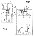
- the vacuum coating system shown serves for the vapor deposition of coating layers on optical substrates 10, such as plastic glasses, which can be clamped onto dome-shaped carrier means 1 in an evacuable recipient 2 above evaporation sources 20 and possibly additional ones Radiate heat radiators 21.
- At least one sensor 3, in particular Temperature sensor, on the rotating carrier means 1 for the substrates 10 is arranged in at least approximately the coating level thereof, the sensor 3 with electrical circuit means 11, 13 in operative connection stands for transformative energy transfer between stationary Part 2 of the coating system and rotating carriers 1.
- the circuit means comprise a primary circuit 11 and one Secondary circuit 13, the primary circuit 11 via a transformer 4 is coupled to the secondary circuit 13 without contact.
- This transformer 4 comprises a primary coil 5 in the primary circuit a stationary core 6 and a secondary coil 7 in the secondary circuit on a core 8 movable relative to the stationary core.
- a voltage source 12 and a are in the primary circuit Evaluation device 16 for the induced measurement data and in the secondary circuit, in addition to the temperature sensor 3 generating measurement data, a Evaluation device 14 digitizing measurement data, the output signals of which are one Control short circuit generator 15.
- the primary coil with the stationary core and the secondary coil with the movable one Core are arranged coaxially and circumferentially relative to each other, such as 1 shows.
- the sensor 3 moved with the secondary circuit 13 now receives its Transformer energy from the primary circuit 11, which from the sensor 3 generated current and voltage measurement data to the evaluation device 14 arrive, the then converted into digital output signals Measurement data control a short-circuit generator 15, which the current in the secondary circuit 13 short-circuits according to the measurement data history.
- Measurement data control a short-circuit generator 15, which the current in the secondary circuit 13 short-circuits according to the measurement data history.
- the one in the primary circuit 11 induced equivalent current and voltage change signals are then usable with the evaluation device 16 in the primary circuit 1 Output signals convertible.
- these measures make it possible to use an electrical one Energy transfer from a stationary primary circuit to a relative one to this movable secondary circuit as well as a retransmission of Measurement data generated in the secondary circuit to the primary circuit in a reasonable way today to allow one in the primary circuit Primary voltage generated and this transformer on the secondary circuit is transmitted and then those generated in the secondary circuit Measurement data digitally transformed and on the same transformer path retransmit the primary circuit and be evaluated there.
- the senor can be of any kind.
- the secondary circuit can continue also include several identical or different sensors.
- the evaluation device and short-circuit generator are then correspondingly in the secondary circuit and to design the evaluation device in the primary circuit.
Landscapes
- Chemical & Material Sciences (AREA)
- Materials Engineering (AREA)
- Metallurgy (AREA)
- Organic Chemistry (AREA)
- Chemical Kinetics & Catalysis (AREA)
- Engineering & Computer Science (AREA)
- Mechanical Engineering (AREA)
- Physics & Mathematics (AREA)
- Optics & Photonics (AREA)
- General Physics & Mathematics (AREA)
- Physical Vapour Deposition (AREA)
- Surface Treatment Of Optical Elements (AREA)
- Polymers With Sulfur, Phosphorus Or Metals In The Main Chain (AREA)
- Agricultural Chemicals And Associated Chemicals (AREA)
- Fertilizers (AREA)
Abstract
Description
- Fig.1
- eine Vakuum-Beschichtungsanlage, im Schnitt, mit einem Temperaturfühler, der mit elektrischen Schaltungsmitteln in Wirkungsverbindung steht zur tranformatorischen Energieübertragung zwischen stillstehendem Teil der Beschichtungsanlage und umlaufenden Trägermitteln; und
- Fig.2
- ein Schaltschema der Schaltungsmittel gemäss Fig. 1 mit einem Primär-Schaltkreis, der über einen Transformator mit einem Sekundär-Schaltkreis berührungsfrei gekoppelt ist.
Claims (7)
- Vakuum-Beschichtungsanlage zum Aufdampfen von Vergütungsschichten auf optische Substrate (10), wie Kunststoff-Brillengläser, welche auf domförmige Trägermittel (1) aufspannbar sind, die in einem evakuierbaren Rezipienten (2) oberhalb von Verdampfungsquellen (20) und gegebenenfalls zusätzlichen Wärmestrahlern (21) umlaufen,
dadurch gekennzeichnet,
dass mindestens ein Messfühler (3), insbesondere Temperaturfühler, an den umlaufenden Trägermitteln (1) für die Substrate (10) in mindestens angenähert deren Beschichtungsebene angeordnet ist, wobei der Messfühler (3) mit elektrischen Schaltungsmitteln (11,13) in Wirkungsverbindung steht zur tranformatorischen Energieübertragung zwischen stillstehendem Teil (2) der Beschichtungsanlage und umlaufenden Trägermitteln (1). - Vakuum-Beschichtungsanlage nach Anspruch 1, dadurch gekennzeichnet, dass die Schaltungsmittel einen Primär-Schaltkreis (11) und einen Sekundär-Schaltkreis (13) umfassen, wobei der Primär-Schaltkreis (11) über einen Transformator (4) mit dem Sekundär-Schaltkreis (13) berührungsfrei gekoppelt ist.
- Vakuum-Beschichtungsanlage nach Anspruch 2, dadurch gekennzeichnet, dass der Transformator (4) eine Primär-Spule (5) im Primär-Schaltkreis auf einem stationären Kern (6) und eine Sekundär-Spule (7) im Sekundär-Schaltkreis auf einem relativ zum stationären Kern bewegbaren Kern (8) umfasst.
- Vakuum-Beschichtungsanlage nach Anspruch 3, dadurch gekennzeichnet, dass sich im Primär-Schaltkreis eine Spannungsquelle (12) sowie eine Auswerteeinrichtung (16) für die induzierten Messdaten befinden und sich im Sekundär-Schaltkreis neben dem Messdaten erzeugenden Temperaturfühler (3) eine die Messdaten digitalisierende Auswerteeinrichtung (14) befindet, deren Ausgangssignale einen Kurzschlusserzeuger (15) steuern.
- Vakuum-Beschichtungsanlage nach Anspruch 3, dadurch gekennzeichnet, dass die Primär-Spule mit dem stationären Kern und die Sekundär-Spule mit dem bewegbaren Kern koaxial und relativ zueinander umlaufend angeordnet sind.
- Vakuum-Beschichtungsanlage nach Anspruch 3, dadurch gekennzeichnet, dass der mit dem Sekundär-Schaltkreis (13) bewegte Messfühler (3) seine Energie transformatorisch aus dem Primär-Schaltkreis (11) erhält, dass die vom Messfühler (3) erzeugten Strom- und Spannungs-Messdaten zu der Auswerteeinrichtung (14) gelangen und dass die in digitale Ausgangssignale umgeformten Messdaten einen Kurzschlusserzeuger (15) steuern, welcher den Strom im Sekundär-Schaltkreis (13) gemäss dem Messdatenverlauf kurzschliesst.
- Vakuum-Beschichtungsanlage nach Anspruch 4 oder 6, dadurch gekennzeichnet, dass die im Primär-Schaltkreis (11) induzierten äquivalenten Strom- und Spannungsänderungssignale über die Auswerteeinrichtung (16) im Primär-Schaltkreis (1) gelangen und dort in verwertbare Ausgangssignale überführbar sind.
Applications Claiming Priority (2)
| Application Number | Priority Date | Filing Date | Title |
|---|---|---|---|
| CH82399 | 1999-05-04 | ||
| CH00823/99A CH693748A5 (de) | 1999-05-04 | 1999-05-04 | Vakuum-Beschichtungsanlage zum Aufdampfen von Verguetungsschichten auf optische Substrate. |
Publications (3)
| Publication Number | Publication Date |
|---|---|
| EP1050598A2 true EP1050598A2 (de) | 2000-11-08 |
| EP1050598A3 EP1050598A3 (de) | 2004-01-21 |
| EP1050598B1 EP1050598B1 (de) | 2005-06-15 |
Family
ID=4196036
Family Applications (1)
| Application Number | Title | Priority Date | Filing Date |
|---|---|---|---|
| EP00107654A Expired - Lifetime EP1050598B1 (de) | 1999-05-04 | 2000-04-10 | Vakuum-Beschichtungsanlage |
Country Status (6)
| Country | Link |
|---|---|
| EP (1) | EP1050598B1 (de) |
| JP (1) | JP2000336472A (de) |
| KR (1) | KR100705527B1 (de) |
| AT (1) | ATE298012T1 (de) |
| CH (1) | CH693748A5 (de) |
| DE (1) | DE50010545D1 (de) |
Families Citing this family (2)
| Publication number | Priority date | Publication date | Assignee | Title |
|---|---|---|---|---|
| KR100980258B1 (ko) * | 2008-03-01 | 2010-09-06 | 주식회사 유성진공 | 다층막 증착장치에 사용되는 증착제품 고정용 돔 |
| JP2023016212A (ja) * | 2021-07-21 | 2023-02-02 | 株式会社昭和真空 | 基板処置装置、基板処理方法、及び光学素子の製造方法 |
Family Cites Families (8)
| Publication number | Priority date | Publication date | Assignee | Title |
|---|---|---|---|---|
| JPS505063B1 (de) * | 1969-05-24 | 1975-02-27 | ||
| JPS50143578U (de) * | 1974-05-15 | 1975-11-27 | ||
| CH668430A5 (de) * | 1986-07-31 | 1988-12-30 | Satis Vacuum Ag | Vakuum-beschichtungsanlage fuer optische substrate. |
| JPH063503A (ja) * | 1992-06-18 | 1994-01-14 | Seiko Epson Corp | 眼鏡用レンズの反射防止膜蒸着装置 |
| US5468299A (en) * | 1995-01-09 | 1995-11-21 | Tsai; Charles S. | Device comprising a flat susceptor rotating parallel to a reference surface about a shaft perpendicular to this surface |
| TW331652B (en) * | 1995-06-16 | 1998-05-11 | Ebara Corp | Thin film vapor deposition apparatus |
| DE19701419A1 (de) * | 1997-01-17 | 1998-07-23 | Geesthacht Gkss Forschung | Substrathaltereinrichtung |
| JP5468299B2 (ja) * | 2009-05-15 | 2014-04-09 | 旭化成ファーマ株式会社 | Impdh含有組成物及びimpdhの安定化方法 |
-
1999
- 1999-05-04 CH CH00823/99A patent/CH693748A5/de not_active IP Right Cessation
-
2000
- 2000-04-10 EP EP00107654A patent/EP1050598B1/de not_active Expired - Lifetime
- 2000-04-10 DE DE50010545T patent/DE50010545D1/de not_active Expired - Lifetime
- 2000-04-10 AT AT00107654T patent/ATE298012T1/de not_active IP Right Cessation
- 2000-04-25 JP JP2000124649A patent/JP2000336472A/ja active Pending
- 2000-05-03 KR KR1020000023622A patent/KR100705527B1/ko not_active Expired - Fee Related
Also Published As
| Publication number | Publication date |
|---|---|
| EP1050598B1 (de) | 2005-06-15 |
| ATE298012T1 (de) | 2005-07-15 |
| JP2000336472A (ja) | 2000-12-05 |
| KR100705527B1 (ko) | 2007-04-10 |
| KR20000077133A (ko) | 2000-12-26 |
| DE50010545D1 (de) | 2005-07-21 |
| EP1050598A3 (de) | 2004-01-21 |
| CH693748A5 (de) | 2004-01-15 |
Similar Documents
| Publication | Publication Date | Title |
|---|---|---|
| EP1462770B1 (de) | Offset-reduzierter Hall-Sensor | |
| DE60126389T2 (de) | Ein verbesserter optischer Querverbindungsschalter | |
| DE3884921T2 (de) | Verfahren zur Temperaturkontrolle einer Halbleiterscheibe auf einer Einspannvorrichtung. | |
| DE69732862T2 (de) | Halbleiteranordnung zur aufnahme von infrarotbildern | |
| EP0023574B1 (de) | Opto-elektronisches Prüfsystem zur automatischen Beschaffenheitsprüfung von Leiterplatten, deren Zwischenprodukte und Druckwerkzeuge | |
| DE102016223215A1 (de) | Bestrahlungseinrichtung und Bearbeitungsmaschine damit | |
| DE102014221829B4 (de) | Verfahren zur Herstellung eines Sensorboards für ein Detektormodul und damit hergestelltes Detektormodul | |
| DE69421522T2 (de) | Verfahren zur reparatur einer leitung eines dünnfilm-bildsensors oder einer dünnfilm-anzeige und die dadurch hergestellte struktur | |
| DE69017529T2 (de) | Bildinformation verarbeitende Vorrichtung. | |
| DE102005047482A1 (de) | Magnetoresistives Sensormodul und Verfahren zum Herstellen desselben | |
| DE3019454A1 (de) | Drahtverbindungsvorrichtung | |
| DE3500645A1 (de) | Fotosensoranordnung | |
| EP0225559A1 (de) | Kontaktbildsensorzeile | |
| EP1050598A2 (de) | Vakuum-Beschichtungsanlage | |
| EP1077129A2 (de) | Verfahren und Vorrichtung zum reversiblen Bebildern einer Druckform | |
| DE102019009361B4 (de) | Widerstandselement-array-schaltung, widerstandselement-array-schaltungseinheit und infrarotsensor | |
| EP0125390A1 (de) | Semitransparente Sensoren sowie deren Herstellung und Anwendung | |
| DE10102540B4 (de) | Anordnung und Verfahren zur Identifikation von Substraten | |
| DE2243979C3 (de) | Magnetoresistive Abfühlanordnung mit Rauschunterdrückung | |
| DE112019006654T5 (de) | Bildgebungsvorrichtung und bildgebungssystem | |
| CH648964A5 (de) | ||
| DE3424785C2 (de) | ||
| DE1904827A1 (de) | Analogspeicher-Verstaerkersystem | |
| EP3526816A1 (de) | Mikrostrukturiertes organisches sensorbauelement und verfahren zu dessen herstellung | |
| DE1622378B2 (de) | Elektrofraktophotographisches oder elektrofraktographisches verfahren |
Legal Events
| Date | Code | Title | Description |
|---|---|---|---|
| PUAI | Public reference made under article 153(3) epc to a published international application that has entered the european phase |
Free format text: ORIGINAL CODE: 0009012 |
|
| AK | Designated contracting states |
Kind code of ref document: A2 Designated state(s): AT BE CH CY DE DK ES FI FR GB GR IE IT LI LU MC NL PT SE |
|
| AX | Request for extension of the european patent |
Free format text: AL;LT;LV;MK;RO;SI |
|
| PUAL | Search report despatched |
Free format text: ORIGINAL CODE: 0009013 |
|
| AK | Designated contracting states |
Kind code of ref document: A3 Designated state(s): AT BE CH CY DE DK ES FI FR GB GR IE IT LI LU MC NL PT SE |
|
| AX | Request for extension of the european patent |
Extension state: AL LT LV MK RO SI |
|
| RIC1 | Information provided on ipc code assigned before grant |
Ipc: 7C 23C 14/50 A Ipc: 7C 23C 14/54 B Ipc: 7G 02B 1/10 B |
|
| 17P | Request for examination filed |
Effective date: 20040721 |
|
| AKX | Designation fees paid |
Designated state(s): AT BE CH CY DE DK ES FI FR GB GR IE IT LI LU MC NL PT SE |
|
| GRAP | Despatch of communication of intention to grant a patent |
Free format text: ORIGINAL CODE: EPIDOSNIGR1 |
|
| GRAS | Grant fee paid |
Free format text: ORIGINAL CODE: EPIDOSNIGR3 |
|
| GRAA | (expected) grant |
Free format text: ORIGINAL CODE: 0009210 |
|
| AK | Designated contracting states |
Kind code of ref document: B1 Designated state(s): AT BE CH CY DE DK ES FI FR GB GR IE IT LI LU MC NL PT SE |
|
| PG25 | Lapsed in a contracting state [announced via postgrant information from national office to epo] |
Ref country code: NL Free format text: LAPSE BECAUSE OF FAILURE TO SUBMIT A TRANSLATION OF THE DESCRIPTION OR TO PAY THE FEE WITHIN THE PRESCRIBED TIME-LIMIT Effective date: 20050615 Ref country code: IE Free format text: LAPSE BECAUSE OF FAILURE TO SUBMIT A TRANSLATION OF THE DESCRIPTION OR TO PAY THE FEE WITHIN THE PRESCRIBED TIME-LIMIT Effective date: 20050615 Ref country code: FI Free format text: LAPSE BECAUSE OF FAILURE TO SUBMIT A TRANSLATION OF THE DESCRIPTION OR TO PAY THE FEE WITHIN THE PRESCRIBED TIME-LIMIT Effective date: 20050615 |
|
| REG | Reference to a national code |
Ref country code: CH Ref legal event code: EP Ref country code: GB Ref legal event code: FG4D Free format text: NOT ENGLISH |
|
| REF | Corresponds to: |
Ref document number: 50010545 Country of ref document: DE Date of ref document: 20050721 Kind code of ref document: P |
|
| REG | Reference to a national code |
Ref country code: IE Ref legal event code: FG4D Free format text: LANGUAGE OF EP DOCUMENT: GERMAN |
|
| GBT | Gb: translation of ep patent filed (gb section 77(6)(a)/1977) |
Effective date: 20050817 |
|
| PG25 | Lapsed in a contracting state [announced via postgrant information from national office to epo] |
Ref country code: SE Free format text: LAPSE BECAUSE OF FAILURE TO SUBMIT A TRANSLATION OF THE DESCRIPTION OR TO PAY THE FEE WITHIN THE PRESCRIBED TIME-LIMIT Effective date: 20050915 Ref country code: DK Free format text: LAPSE BECAUSE OF FAILURE TO SUBMIT A TRANSLATION OF THE DESCRIPTION OR TO PAY THE FEE WITHIN THE PRESCRIBED TIME-LIMIT Effective date: 20050915 Ref country code: GR Free format text: LAPSE BECAUSE OF FAILURE TO SUBMIT A TRANSLATION OF THE DESCRIPTION OR TO PAY THE FEE WITHIN THE PRESCRIBED TIME-LIMIT Effective date: 20050915 |
|
| PG25 | Lapsed in a contracting state [announced via postgrant information from national office to epo] |
Ref country code: ES Free format text: LAPSE BECAUSE OF FAILURE TO SUBMIT A TRANSLATION OF THE DESCRIPTION OR TO PAY THE FEE WITHIN THE PRESCRIBED TIME-LIMIT Effective date: 20050926 |
|
| PG25 | Lapsed in a contracting state [announced via postgrant information from national office to epo] |
Ref country code: PT Free format text: LAPSE BECAUSE OF FAILURE TO SUBMIT A TRANSLATION OF THE DESCRIPTION OR TO PAY THE FEE WITHIN THE PRESCRIBED TIME-LIMIT Effective date: 20051123 |
|
| NLV1 | Nl: lapsed or annulled due to failure to fulfill the requirements of art. 29p and 29m of the patents act | ||
| REG | Reference to a national code |
Ref country code: IE Ref legal event code: FD4D |
|
| ET | Fr: translation filed | ||
| PG25 | Lapsed in a contracting state [announced via postgrant information from national office to epo] |
Ref country code: AT Free format text: LAPSE BECAUSE OF NON-PAYMENT OF DUE FEES Effective date: 20060410 |
|
| PG25 | Lapsed in a contracting state [announced via postgrant information from national office to epo] |
Ref country code: BE Free format text: LAPSE BECAUSE OF NON-PAYMENT OF DUE FEES Effective date: 20060430 Ref country code: CH Free format text: LAPSE BECAUSE OF NON-PAYMENT OF DUE FEES Effective date: 20060430 Ref country code: LI Free format text: LAPSE BECAUSE OF NON-PAYMENT OF DUE FEES Effective date: 20060430 Ref country code: MC Free format text: LAPSE BECAUSE OF NON-PAYMENT OF DUE FEES Effective date: 20060430 |
|
| PLBE | No opposition filed within time limit |
Free format text: ORIGINAL CODE: 0009261 |
|
| STAA | Information on the status of an ep patent application or granted ep patent |
Free format text: STATUS: NO OPPOSITION FILED WITHIN TIME LIMIT |
|
| 26N | No opposition filed |
Effective date: 20060316 |
|
| REG | Reference to a national code |
Ref country code: CH Ref legal event code: PL |
|
| BERE | Be: lapsed |
Owner name: SATIS VACUUM INDUSTRIES VERTRIEBS - A.G. Effective date: 20060430 |
|
| PG25 | Lapsed in a contracting state [announced via postgrant information from national office to epo] |
Ref country code: LU Free format text: LAPSE BECAUSE OF NON-PAYMENT OF DUE FEES Effective date: 20060410 |
|
| PG25 | Lapsed in a contracting state [announced via postgrant information from national office to epo] |
Ref country code: CY Free format text: LAPSE BECAUSE OF FAILURE TO SUBMIT A TRANSLATION OF THE DESCRIPTION OR TO PAY THE FEE WITHIN THE PRESCRIBED TIME-LIMIT Effective date: 20050615 |
|
| REG | Reference to a national code |
Ref country code: FR Ref legal event code: CD Ref country code: FR Ref legal event code: CA |
|
| PGFP | Annual fee paid to national office [announced via postgrant information from national office to epo] |
Ref country code: GB Payment date: 20140530 Year of fee payment: 15 |
|
| PGFP | Annual fee paid to national office [announced via postgrant information from national office to epo] |
Ref country code: IT Payment date: 20140424 Year of fee payment: 15 Ref country code: FR Payment date: 20140411 Year of fee payment: 15 Ref country code: DE Payment date: 20140422 Year of fee payment: 15 |
|
| REG | Reference to a national code |
Ref country code: DE Ref legal event code: R119 Ref document number: 50010545 Country of ref document: DE |
|
| GBPC | Gb: european patent ceased through non-payment of renewal fee |
Effective date: 20150410 |
|
| PG25 | Lapsed in a contracting state [announced via postgrant information from national office to epo] |
Ref country code: GB Free format text: LAPSE BECAUSE OF NON-PAYMENT OF DUE FEES Effective date: 20150410 Ref country code: DE Free format text: LAPSE BECAUSE OF NON-PAYMENT OF DUE FEES Effective date: 20151103 Ref country code: IT Free format text: LAPSE BECAUSE OF NON-PAYMENT OF DUE FEES Effective date: 20150410 |
|
| REG | Reference to a national code |
Ref country code: FR Ref legal event code: ST Effective date: 20151231 |
|
| PG25 | Lapsed in a contracting state [announced via postgrant information from national office to epo] |
Ref country code: FR Free format text: LAPSE BECAUSE OF NON-PAYMENT OF DUE FEES Effective date: 20150430 |