EP1046891A2 - Vorrichtung zum Abgleichen einer Messbrückenschaltung und Drehmomentmesswelle - Google Patents
Vorrichtung zum Abgleichen einer Messbrückenschaltung und Drehmomentmesswelle Download PDFInfo
- Publication number
- EP1046891A2 EP1046891A2 EP00106538A EP00106538A EP1046891A2 EP 1046891 A2 EP1046891 A2 EP 1046891A2 EP 00106538 A EP00106538 A EP 00106538A EP 00106538 A EP00106538 A EP 00106538A EP 1046891 A2 EP1046891 A2 EP 1046891A2
- Authority
- EP
- European Patent Office
- Prior art keywords
- trimming
- resistors
- bridge circuit
- printed
- area
- Prior art date
- Legal status (The legal status is an assumption and is not a legal conclusion. Google has not performed a legal analysis and makes no representation as to the accuracy of the status listed.)
- Granted
Links
Images


Classifications
-
- G—PHYSICS
- G01—MEASURING; TESTING
- G01L—MEASURING FORCE, STRESS, TORQUE, WORK, MECHANICAL POWER, MECHANICAL EFFICIENCY, OR FLUID PRESSURE
- G01L3/00—Measuring torque, work, mechanical power, or mechanical efficiency, in general
- G01L3/02—Rotary-transmission dynamometers
- G01L3/04—Rotary-transmission dynamometers wherein the torque-transmitting element comprises a torsionally-flexible shaft
- G01L3/10—Rotary-transmission dynamometers wherein the torque-transmitting element comprises a torsionally-flexible shaft involving electric or magnetic means for indicating
- G01L3/108—Rotary-transmission dynamometers wherein the torque-transmitting element comprises a torsionally-flexible shaft involving electric or magnetic means for indicating involving resistance strain gauges
-
- G—PHYSICS
- G01—MEASURING; TESTING
- G01R—MEASURING ELECTRIC VARIABLES; MEASURING MAGNETIC VARIABLES
- G01R17/00—Measuring arrangements involving comparison with a reference value, e.g. bridge
- G01R17/02—Arrangements in which the value to be measured is automatically compared with a reference value
- G01R17/06—Automatic balancing arrangements
-
- G—PHYSICS
- G01—MEASURING; TESTING
- G01L—MEASURING FORCE, STRESS, TORQUE, WORK, MECHANICAL POWER, MECHANICAL EFFICIENCY, OR FLUID PRESSURE
- G01L25/00—Testing or calibrating of apparatus for measuring force, torque, work, mechanical power, or mechanical efficiency
- G01L25/003—Testing or calibrating of apparatus for measuring force, torque, work, mechanical power, or mechanical efficiency for measuring torque
Definitions
- the invention relates to a device for adjusting a measuring bridge circuit with at least two layer-like printed on a substrate electrical trimming resistors with also printed contacts, whose resistance values for balancing the bridge circuit Incisions in the resistance material are changeable, as well as a torque measuring shaft.
- Thick film resistors are used in arrangements for measuring the elastic strain of mechanical components, such as for monitoring torsional moment on steering columns are used in motor vehicles. Such resistors are on the relevant component including the complete wiring is printed on and are therefore very easy and inexpensive to manufacture in large quantities. Because of of manufacturing tolerances must be ways to match the printed Circuits are provided. The one on the circuits, mostly If Wheatstone bridges are involved, the adjustment to be carried out is either on the bridge resistors themselves, or on specially designed ones Trimmer resistances performed.
- the object of the present invention is to provide a device which is inexpensive to manufacture and saves space and enables precise adjustment.
- the invention is based on the knowledge that these requirements are met can be satisfied if the geometric shape and the connection the trimming resistors are designed so that the imaginary electrical Streamlines in the balanced state essentially along one middle direction. This means that the streamlines through the Incision can be forced to convergence or divergence, on average, however, not be deflected by large angles, but along run in a central direction through the cut. In this way, an essentially straight, unbroken line in the middle direction between the two Pull the contacts of each resistor.
- At least a balancing resistor essentially has an elongated basic shape, that a first connector at one end and a second connector arranged at least partially along the trimming resistor is and that a trimming cut is substantially parallel to and with little Distance from the second connection contact is to be arranged.
- a trimming resistor is formed by a resistance layer one side of which has at least one connection contact and on the opposite side Page essentially parallel to it at least two more Terminal contacts are arranged, the resistance layer for adjustment can be divided into two differently sized areas using a matching cut is, so that there are two resistors of different resistance values.
- This embodiment of the invention is in addition to use as a voltage balancer a bridge circuit also advantageous for voltage distribution usable by the two resistors in a manner known per se can be switched as a voltage divider.
- the Geometric shape of at least one balancing resistor in the unbalanced State composed of two areas that the first area is such it is formed that there the average length of the imaginary electrical current lines between the connection contacts is smaller than the average width of the resistance layer (sub-square) and that the second area is formed in such a way is that there is the mean length of the imaginary electrical current lines between the connection contacts is greater than the average width of the resistance layer (over-square).
- Such a form is in a first embodiment of the invention formed that in each case a first connection contact of at least one trimming resistor this is at least two sides essentially L-shaped to C-shaped surrounds that the second connection contact is arranged inside this shape, including a short leg of the first contact including of the sub-square area essentially parallel with a distance faces that is less than the length of the short leg, and that the area between the contacts filled with resistance material is.
- This geometric shape of the resistors has proven very useful in the experiment proven appropriate.
- the streamlines run in this embodiment the invention without much interference, what the cut very well makes controllable.
- the influence of the cutting length on the change in resistance is linear, the slope in the sub-square area is small because the rest of the resistor is like a resistor in parallel acts and thus reduces the slope.
- the trimming resistors according to the invention have a small one
- the basic resistance with this cut is initially quite flat, linear Characteristic on. So the resistance value in this area can be very sensitive can be controlled by continuously extending the adjustment cut. If the adjustment cut is continued in the vertical area, the Characteristic curve somewhat steeper, but remains essentially linear. So there is a big one Setting range available with a relatively small space requirement and high Setting accuracy.
- two trimming resistors a single structure are united by two of the contacts of the Resistors are combined into a single, central connection contact.
- This measure makes circuits considerably simpler, since there are no longer four, but only three connecting lines for each pair of resistors must be performed.
- the space requirement decreases because of the area for a complete connection contact and otherwise for manufacturing reasons necessary space between the resistors can be saved.
- the pair of resistors can also because of its small size The whole can be arranged in a stretch-neutral area of the component, which is why further measures to compensate for interference are not required can.
- At least one measuring bridge circuit made of strain-sensitive Resistors arranged on a torque measuring shaft as a substrate is that a pair of trimming resistors after a of the preceding claims printed in thick-film technology on the substrate and are connected to the bridge circuits for adjustment.
- the Torque measuring shaft is exposed to a torque to be measured. Out the surface elongation of the shaft measured by the bridge circuits can on their torsional deformation and thus on the applied torque getting closed.
- the trimming resistors arranged in a stretch-neutral region of the substrate are.
- the trimming resistors are on the neutral fiber of the component to be monitored. If this is not possible, you can the trimming resistors are also arranged symmetrically to the neutral fiber so that the effects of expansion are compensated for.
- the trimming resistors to be made from a material that is stretchable and temperature changes have a low and constant sensitivity.
- the trimming resistors Ranges of different resistance values are composed, whereby the areas can advantageously be arranged such that the area subdivision runs essentially along the central direction of the streamlines.
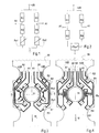
- FIG. 1 shows a conventional bridge circuit for measuring material expansions, those with four strain-sensitive resistors R1 to R4, as well with two trimming resistors Rv1 and Rv2 for trimming the zero voltage between the connections A1 and A2.
- Fig. 2 is the same bridge circuit with an inventive Pair Rv of trimming resistors shown.
- the pair of resistors Rv can also consist of a one-piece resistance layer, wherein in in this case the adjustment by a single cut for both resistance values is made.
- the resistance material printed on a substrate The trimming resistors are used for this purpose by means of a laser beam evaporated along the cutting line.
- Fig. 3 shows the arrangement of two measuring bridges, consisting of strain-dependent Resistors R1 to R4, for measuring a torque MT with conventional hat resistors Rv1 and Rv2 as trimming resistors.
- the Circuit is on a steel torsion shaft 30 with a rectangular cross section printed on.
- the shaft converts a torsional moment into a longitudinal one Expansion of the expansion-dependent resistors R1 to R4.
- the shaft 30 is provided with various recesses 31.
- the hat resistors Rv1 and Rv2 are used to adjust the measuring bridges Provide adjustment cuts S.
- the voltage relationships of the bridge circuits can be used for exact adjustment during the cutting process continuously be measured.
- the trimming resistors are used to compensate for Strain influences symmetrical to the strain neutral area the shaft 30 arranged.
- FIG. 4 shows the same arrangement with the aid of two pairs Rv according to the invention realized by trimming resistors.
- the cable routing is essential here easier than when using individual resistors.
- the trimming resistors Rv can be placed directly on the strain neutral fiber of the shaft are so that strain influences are excluded. Furthermore, this causes crack formation on the adjustment cuts S due to permanent alternating loads avoided.
- the intended arrangement of the resistance material 60 between the connection contacts 61, 62 is shown in Fig. 6a).
- a further improvement of the adjustment can be achieved by an arrangement as shown in Fig. 6b) and Fig. 6c).
- the balancing resistance 65 from a sub-square area between the horizontal Sections of the contacts 64 and 65 and an oversquare Area along the long leg of the contact 65.
- the first adjustment resistor is used for rough adjustment 63 a section according to FIG. 6c) is performed.
- a second Trimming resistor 63 is then cut in according to FIG. 6b) for fine adjustment.
- FIG. 7 shows trimming resistors assembled to form a pair of resistors 70.
- Such an arrangement takes up even less space than that previously and can therefore be used as a whole in a stretch-neutral range be arranged on a component to be monitored. Simplified further the wiring of the bridge circuit built up with it considerably only three connection lines are necessary, which are connected to the three connection contacts 71, 72 are introduced.
- FIG. 8 Another possibility, the undisturbed streamline course according to the invention to achieve is shown in Fig. 8.
- a one piece resistor 80 which is between parallel connection contacts 81, 82 is embedded for adjustment cut in a predetermined place. This creates two Resistors of different resistance values, the trimming resistors represent. This arrangement can advantageously also be compared Voltage dividers are used.
- the characteristic curve R (x) of the trimming resistor 60 is shown in FIG. R denotes the resistance value, x the length of the adjustment section S. Between With the coordinates xmin and xmax, the characteristic curve is approximately linear, see above that a precise and simple comparison is possible here.
- FIG. 10 shows the characteristic curve of the trimming resistor according to FIG. 6b) and FIG. 6c).
- the individual sections of the characteristic curve run approximately linear.
- FIG. 11 Further exemplary embodiments of trimming resistors according to the invention are shown in Fig. 11.
- Figures 11a) to 11c) show further one-piece trimming resistors at which the resistance layer W by a straight trimming cut in two Resistors of different resistance values can be subdivided.
- the resistances are each via the connection contacts A, B and C with a circuit connectable.
- the streamlines i also run essentially with these resistors along a central direction between the respective connection contacts.
- the resistance layer W is of a ring shape in the raw state
- Conductor 111 surrounded by laser cuts SA in the connection contacts A, B and C can be subdivided.
- 11b) are conductor loops 110 is provided, which on the provided for possible alignment cuts Points are arranged and can be divided by separating cuts SA, so that the connection contacts A and B arise. Allow the loops it, the cut through the conductive material of the connection contacts with higher Perform laser power than it is for the resistive material Due to the accuracy of the adjustment is required. In the event that no adjustment the conductor loops are not cut.
- Figures 11d) to 11f) show further paired adjustment resistors, the each consist of two modified resistors according to FIG. 6a).
- the two Resistance elements W1 and W2 are each pairwise resistor by means of a centrally arranged connection contact to form a pair connected.
- the trimming resistor of FIG. 11e) again points out the above Establish conductor loops 110, which are severed for adjustment.
- Fig. 12 shows a trimming resistor which is different from two areas W, W ' Resistance materials is composed.
- the area W points a resistance value ten times higher than the range W '.
- the Resistance itself again has a sub-square area 121 and one square area 122.
- a matching cut is made so that it cuts through area W after a start in area 121 in order to to achieve a high adjustment speed there and shortly before reaching it of the matching target changes into the area W ', and there the matching target continues controls. This enables a very fine adjustment with a single cut.
- FIG. 13 shows the resistance characteristic of the trimming resistor shown in FIG. 12.
- the characteristic curve runs flat in sub-square area (131), then first by changing over to become steeper in the over-square area W (132). After switching in the area W 'runs flat again.
- the adjustment cut is to be carried out to position xE.
Landscapes
- Physics & Mathematics (AREA)
- General Physics & Mathematics (AREA)
- Apparatuses And Processes For Manufacturing Resistors (AREA)
- Measuring Instrument Details And Bridges, And Automatic Balancing Devices (AREA)
- Length Measuring Devices With Unspecified Measuring Means (AREA)
- Measurement Of Length, Angles, Or The Like Using Electric Or Magnetic Means (AREA)
Abstract
Description
- Fig. 1
- eine Brückenschaltung mit herkömmlichen Abgleichwiderständen,
- Fig. 2
- eine Brückenschaltung mit einem erfindungsgemäßen Paar von Abgleichwiderständen,
- Fig. 3
- eine Drehmomentmeßwelle mit in Dickschichttechnik gedruckter Meßschaltung mit herkömmlichen Abgleichwiderständen,
- Fig. 4
- eine Drehmomentmeßwelle mit in Dickschichttechnik gedruckter Meßschaltung mit erfindungsgemäßen Paaren von Abgleichwiderständen,
- Fig. 5
- einen herkömmlichen Abgleichwiderstand,
- Fig. 6
- erfindungsgemäße einzelne Abgleichwiderstände,
- Fig. 7
- ein erfindungsgemäßes Paar von Abgleichwiderständen,
- Fig. 8
- einen erfindungsgemäßen einstückigen Abgleichwiderstand,
- Fig. 9
- die Kennlinie des Abgleichwiderstands nach Fig. 6a),
- Fig. 10
- die Kennlinie des Abgleichwiderstands nach Fig. 6b) und 6c),
- Fig. 11
- weitere Ausführungsbeispiele erfindungsgemäßer Abgleichwiderstände,
- Fig. 12
- einen Abgleichwiderstand mit zwei verschiedenen Widerstandsmaterialien und
- Fig. 13
- die dazu gehörige Schnittlängen-Widerstands-Kennlinie.
Claims (13)
- Vorrichtung zum Abgleichen einer Meßbrückenschaltung mit wenigstens zwei auf einem Substrat aufgedruckten schichtartigen elektrischen Abgleichwiderständen mit ebenfalls aufgedruckten Anschlußkontakten, deren Widerstandswerte zum Abgleich der Brückenschaltung durch Einschnitte in das Widerstandsmaterial veränderbar sind, dadurch gekennzeichnet, daß die geometrische Form und die Anschlußkontaktierung der Abgleichwiderstände derart angelegt sind, daß die gedachten elektrischen Stromlinien im abgeglichenen Zustand im wesentlichen entlang einer mittleren Richtung verlaufen.
- Vorrichtung zum Abgleichen einer Meßbrückenschaltung mit wenigstens zwei auf einem Substrat aufgedruckten schichtartigen elektrischen Abgleichwiderständen mit ebenfalls aufgedruckten Anschlußkontakten, deren Widerstandswerte zum Abgleich der Brückenschaltung durch Einschnitte in das Widerstandsmaterial veränderbar sind, dadurch gekennzeichnet, daß wenigstens ein Abgleichwiderstand (60) im wesentlichen eine längliche Grundform aufweist, daß ein erster Anschlußkontakt (61) an einem Ende und ein zweiter Anschlußkontakt (62) wenigstens teilweise längs des Abgleichwiderstands (60) angeordnet ist und daß ein Abgleichschnitt (S) im wesentlichen parallel zu und mit geringem Abstand von dem zweiten Anschlußkontakt (62) anzuordnen ist.
- Vorrichtung zum Abgleichen einer Meßbrückenschaltung mit wenigstens zwei auf einem Substrat aufgedruckten schichtartigen elektrischen Abgleichwiderständen mit ebenfalls aufgedruckten Anschlußkontakten, deren Widerstandswerte zum Abgleich der Brückenschaltung durch Einschnitte in das Widerstandsmaterial veränderbar sind, dadurch gekennzeichnet, daß wenigstens ein Abgleichwiderstand (80) durch eine Widerstandsschicht (80) gebildet ist, auf deren einer Seite wenigstens ein Anschlußkontakt (82) und auf der dieser Seite gegenüberliegenden Seite im wesentlichen parallel dazu wenigstens zwei weitere Anschlußkontakte angeordnet sind, wobei die Widerstandsschicht (80) zum Abgleich durch einen Abgleichschnitt (S) in zwei unterschiedlich große Bereiche teilbar ist, so daß sich zwei Widerstände unterschiedlicher Widerstandswerte ergeben.
- Vorrichtung zum Abgleichen einer Meßbrückenschaltung mit wenigstens zwei auf einem Substrat aufgedruckten schichtartigen elektrischen Abgleichwiderständen mit ebenfalls aufgedruckten Anschlußkontakten, deren Widerstandswerte zum Abgleich der Brückenschaltung durch Einschnitte in das Widerstandsmaterial veränderbar sind, dadurch gekennzeichnet, daß die geometrische Form wenigstens eines Abgleichwiderstands (63) im unabgeglichenen Zustand aus zwei Bereichen (63', 63'') zusammengesetzt ist, daß der erste Bereich (63') derart ausgebildet ist, daß dort die mittlere Länge der gedachten elektrischen Stromlinien (i) zwischen den Anschlußkontakten (64, 65) kleiner ist als die mittlere Breite (l) der Widerstandsschicht (63) (unterquadratisch) und daß der zweite Bereich (63'') derart ausgebildet ist, daß dort die mittlere Länge der gedachten elektrischen Stromlinien (i) zwischen den Anschlußkontakten (64, 65) größer ist als die mittlere Breite der Widerstandsschicht (63) (überquadratisch).
- Vorrichtung nach Anspruch 4, dadurch gekennzeichnet, daß jeweils ein erster Anschlußkontakt (65) wenigstens eines Abgleichwiderstands (63) diesen an wenigstens zwei Seiten im wesentlichen L- bis C-förmig umgibt, daß der zweite Anschlußkontakt (64) im Innern dieser Form (65) angeordnet ist, wobei er einem kurzen Schenkel des ersten Anschlußkontakts (65) unter Einschluß des unterquadratischen Bereichs (63') im wesentlichen parallel mit einem Abstand gegenübersteht, der geringer ist als die Länge (l) des kurzen Schenkels, und daß der Bereich (63', 63'') zwischen den Anschlußkontakten (64, 65) mit Widerstandsmaterial (63) ausgefüllt ist.
- Vorrichtung nach Anspruch 3, dadurch gekennzeichnet, daß wenigstens in einem Anfangsbereich (63') ein Abgleichschnitt (S) im wesentlichen parallel zu dem kurzen Schenkel verläuft.
- Vorrichtung nach Anspruch 6, dadurch gekennzeichnet, daß der Abgleichschnitt (S) in einem weiteren, an den Anfangsbereich anschließenden Bereich (63'') im wesentlichen parallel zu dem langen Schenkel verläuft.
- Vorrichtung nach einem der vorhergehenden Ansprüche, dadurch gekennzeichnet, daß zwei Abgleichwiderstände zu einer einzigen Struktur vereinigt sind, indem zwei der Anschlußkontakte der Widerstände zu einem einzigen, zentralen Anschlußkontakt vereinigt sind.
- Vorrichtung nach einem der vorhergehenden Ansprüche, dadurch gekennzeichnet, daß wenigstens eine Meßbrückenschaltung aus dehnungsempfindlichen Widerständen (R1 bis R4) auf einer Momentenmeßwelle (30) als Substrat angeordnet ist, daß je Brückenschaltung ein Paar (Rv) von Abgleichwiderständen nach einem der vorhergehenden Ansprüche in Dickschichttechnik auf dem Substrat (30) aufgedruckt und mit den Brückenschaltungen zum Abgleich verschaltet sind.
- Vorrichtung nach einem der vorhergehenden Ansprüche, dadurch gekennzeichnet, daß die Abgleichwiderstände in einem dehnungsneutralen Bereich des Substrats (30) angeordnet sind.
- Vorrichtung nach einem der vorhergehenden Ansprüche, dadurch gekennzeichnet, daß die Abgleichwiderstände aus Bereichen (W, W') unterschiedlicher Widerstandswerte zusammengesetzt sind.
- Vorrichtung nach Anspruch 11, dadurch gekennzeichnet, daß die Bereichsunterteilung im wesentlichen längs der mittleren Richtung der Stromlinien verläuft.
- Vorrichtung nach einem der vorhergehenden Ansprüche 11 oder 12, dadurch gekennzeichnet, daß ein Abgleichschnitt nach Durchschneiden eines Bereichs hohen spezifischen Widerstands (W) in einem Bereich niedrigen spezifischen Widerstands (W') endet.
Applications Claiming Priority (2)
| Application Number | Priority Date | Filing Date | Title |
|---|---|---|---|
| DE19917443 | 1999-04-17 | ||
| DE19917443A DE19917443A1 (de) | 1999-04-17 | 1999-04-17 | Abgleichwiderstand und Drehmomentmeßwelle |
Publications (3)
| Publication Number | Publication Date |
|---|---|
| EP1046891A2 true EP1046891A2 (de) | 2000-10-25 |
| EP1046891A3 EP1046891A3 (de) | 2001-05-23 |
| EP1046891B1 EP1046891B1 (de) | 2002-12-11 |
Family
ID=7904950
Family Applications (1)
| Application Number | Title | Priority Date | Filing Date |
|---|---|---|---|
| EP00106538A Expired - Lifetime EP1046891B1 (de) | 1999-04-17 | 2000-03-27 | Vorrichtung zum Abgleichen einer Messbrückenschaltung und Drehmomentmesswelle |
Country Status (5)
| Country | Link |
|---|---|
| EP (1) | EP1046891B1 (de) |
| JP (1) | JP2000329794A (de) |
| KR (1) | KR20010014743A (de) |
| AT (1) | ATE229644T1 (de) |
| DE (2) | DE19917443A1 (de) |
Cited By (1)
| Publication number | Priority date | Publication date | Assignee | Title |
|---|---|---|---|---|
| KR20010014743A (ko) * | 1999-04-17 | 2001-02-26 | 요한 요트너,헤르베르트 코네감프 | 평형 저항 및 회전모멘트 측정축 |
Family Cites Families (11)
| Publication number | Priority date | Publication date | Assignee | Title |
|---|---|---|---|---|
| DD109466A1 (de) * | 1974-01-25 | 1974-11-05 | ||
| DE2555226C3 (de) * | 1975-12-09 | 1982-04-29 | Daimler-Benz Ag, 7000 Stuttgart | Anordnung zur elektronischen Kalibrierung von an rotierenden Elementen angeordneten Meßeinrichtungen |
| DE2724817A1 (de) * | 1977-06-02 | 1978-12-07 | Philips Patentverwaltung | Verfahren zum abgleichen einer dehnungsmesstreifenvollbruecke |
| US4505032A (en) * | 1983-06-27 | 1985-03-19 | Analogic Corporation | Method of making a voltage divider |
| DE3544984A1 (de) * | 1985-12-19 | 1987-06-25 | Bosch Gmbh Robert | Abgleichbarer widerstand |
| US4907460A (en) * | 1987-10-30 | 1990-03-13 | Koyo Seiko Co., Ltd. | Torque sensor |
| KR970005700Y1 (ko) * | 1994-04-14 | 1997-06-10 | 최동길 | 밸런스 장치 |
| DE19547352B4 (de) * | 1995-12-19 | 2004-10-14 | Hottinger Baldwin Messtechnik Gmbh | Einrichtung zum Messen von Kräften und/oder Momenten |
| DE19548563A1 (de) * | 1995-12-23 | 1997-06-26 | Vdo Schindling | Verfahren zum Abgleich von Widerständen |
| JPH11101816A (ja) * | 1997-09-29 | 1999-04-13 | Mazda Motor Corp | 角加速度センサ及び角加速度検出方法 |
| DE19917443A1 (de) * | 1999-04-17 | 2000-10-19 | Mannesmann Vdo Ag | Abgleichwiderstand und Drehmomentmeßwelle |
-
1999
- 1999-04-17 DE DE19917443A patent/DE19917443A1/de not_active Withdrawn
-
2000
- 2000-03-27 AT AT00106538T patent/ATE229644T1/de not_active IP Right Cessation
- 2000-03-27 DE DE50000897T patent/DE50000897D1/de not_active Expired - Fee Related
- 2000-03-27 EP EP00106538A patent/EP1046891B1/de not_active Expired - Lifetime
- 2000-04-14 JP JP2000113868A patent/JP2000329794A/ja active Pending
- 2000-04-17 KR KR1020000019978A patent/KR20010014743A/ko not_active Ceased
Cited By (1)
| Publication number | Priority date | Publication date | Assignee | Title |
|---|---|---|---|---|
| KR20010014743A (ko) * | 1999-04-17 | 2001-02-26 | 요한 요트너,헤르베르트 코네감프 | 평형 저항 및 회전모멘트 측정축 |
Also Published As
| Publication number | Publication date |
|---|---|
| EP1046891A3 (de) | 2001-05-23 |
| DE19917443A1 (de) | 2000-10-19 |
| DE50000897D1 (de) | 2003-01-23 |
| JP2000329794A (ja) | 2000-11-30 |
| EP1046891B1 (de) | 2002-12-11 |
| ATE229644T1 (de) | 2002-12-15 |
| KR20010014743A (ko) | 2001-02-26 |
Similar Documents
| Publication | Publication Date | Title |
|---|---|---|
| DE69409614T2 (de) | Elektrischer Widerstand | |
| DE3401587C2 (de) | Meßwandler zum Messen eines Stromes | |
| EP0858665A1 (de) | In hybridtechnik hergestellte abgleichbare spannungsteiler-anordnung | |
| EP1324063B1 (de) | Magnetoresistiver Sensor | |
| DE19843579C2 (de) | Mechanisch-elektrischer Wandler | |
| EP2446449A1 (de) | Strommesswiderstand | |
| DE102007001847A1 (de) | Stromsensor und Verfahren zum Montieren desselben | |
| EP0250620B1 (de) | Verfahren und Vorrichtung zum elektrischen Prüfen von Leiterplatten | |
| DE3203334A1 (de) | Kraftmesseinrichtung zur steuerung der position eines von einer landwirtschaftlichen maschine zu schleppenden werkzeugs | |
| DE3218577A1 (de) | Kraftwandler | |
| DE3340720C2 (de) | Spannungsteiler mit mindestens einem stromlosen Abgriff und Verfahren zu seiner Herstellung | |
| DE19722834A1 (de) | Magnetoresistives Gradiometer in Form einer Wheatstone-Brücke zur Messung von Magnetfeldgradienten | |
| EP1046891B1 (de) | Vorrichtung zum Abgleichen einer Messbrückenschaltung und Drehmomentmesswelle | |
| DE2923799C2 (de) | Diffundierter Halbleiterwiderstand | |
| DE2840278A1 (de) | Einstellbare daempfungsvorrichtung | |
| DE3740872C2 (de) | ||
| DE68925117T2 (de) | Insbesondere für temperaturmessung gedachter thermistor und verfahren zur herstellung | |
| DE19826411C2 (de) | Dehnungsmeßstreifen | |
| EP0450107B1 (de) | Verfahren zum Herstellen eines Widerstandselementes | |
| DE68906044T2 (de) | Supraleitende logische vorrichtung. | |
| DE102010029074B4 (de) | Anbindungsstruktur für Mikroschwingeneinrichtungen | |
| EP0188771A2 (de) | Magnetfeldsensor | |
| DE69530253T2 (de) | Magnetoresistiver Strommesser | |
| EP3738211B1 (de) | Verfahren zur bestimmung der auslenkung des betätigungsglieds eines kapazitiven mehrwege-kraftsensorbausteins | |
| DE2651071B2 (de) | Verfahren zur Herstellung eines abgeglichenen Widerstandes in Dickschichttechnik |
Legal Events
| Date | Code | Title | Description |
|---|---|---|---|
| PUAI | Public reference made under article 153(3) epc to a published international application that has entered the european phase |
Free format text: ORIGINAL CODE: 0009012 |
|
| AK | Designated contracting states |
Kind code of ref document: A2 Designated state(s): AT DE FR GB |
|
| AX | Request for extension of the european patent |
Free format text: AL;LT;LV;MK;RO;SI |
|
| PUAL | Search report despatched |
Free format text: ORIGINAL CODE: 0009013 |
|
| AK | Designated contracting states |
Kind code of ref document: A3 Designated state(s): AT BE CH CY DE DK ES FI FR GB GR IE IT LI LU MC NL PT SE |
|
| AX | Request for extension of the european patent |
Free format text: AL;LT;LV;MK;RO;SI |
|
| RIC1 | Information provided on ipc code assigned before grant |
Free format text: 7G 01L 1/22 A, 7G 01L 3/10 B, 7G 01R 17/00 B, 7H 01C 17/24 B |
|
| 17P | Request for examination filed |
Effective date: 20010414 |
|
| 17Q | First examination report despatched |
Effective date: 20010720 |
|
| RAP1 | Party data changed (applicant data changed or rights of an application transferred) |
Owner name: SIEMENS AKTIENGESELLSCHAFT |
|
| GRAG | Despatch of communication of intention to grant |
Free format text: ORIGINAL CODE: EPIDOS AGRA |
|
| AKX | Designation fees paid |
Free format text: AT DE FR GB |
|
| GRAG | Despatch of communication of intention to grant |
Free format text: ORIGINAL CODE: EPIDOS AGRA |
|
| GRAH | Despatch of communication of intention to grant a patent |
Free format text: ORIGINAL CODE: EPIDOS IGRA |
|
| GRAG | Despatch of communication of intention to grant |
Free format text: ORIGINAL CODE: EPIDOS AGRA |
|
| GRAH | Despatch of communication of intention to grant a patent |
Free format text: ORIGINAL CODE: EPIDOS IGRA |
|
| GRAH | Despatch of communication of intention to grant a patent |
Free format text: ORIGINAL CODE: EPIDOS IGRA |
|
| GRAA | (expected) grant |
Free format text: ORIGINAL CODE: 0009210 |
|
| AK | Designated contracting states |
Kind code of ref document: B1 Designated state(s): AT DE FR GB |
|
| REF | Corresponds to: |
Ref document number: 229644 Country of ref document: AT Date of ref document: 20021215 Kind code of ref document: T |
|
| REG | Reference to a national code |
Ref country code: GB Ref legal event code: FG4D Free format text: NOT ENGLISH |
|
| GRAH | Despatch of communication of intention to grant a patent |
Free format text: ORIGINAL CODE: EPIDOS IGRA |
|
| REF | Corresponds to: |
Ref document number: 50000897 Country of ref document: DE Date of ref document: 20030123 |
|
| GBT | Gb: translation of ep patent filed (gb section 77(6)(a)/1977) |
Effective date: 20030315 |
|
| ET | Fr: translation filed | ||
| PLBE | No opposition filed within time limit |
Free format text: ORIGINAL CODE: 0009261 |
|
| STAA | Information on the status of an ep patent application or granted ep patent |
Free format text: STATUS: NO OPPOSITION FILED WITHIN TIME LIMIT |
|
| 26N | No opposition filed |
Effective date: 20030912 |
|
| PGFP | Annual fee paid to national office [announced via postgrant information from national office to epo] |
Ref country code: AT Payment date: 20060310 Year of fee payment: 7 |
|
| PGFP | Annual fee paid to national office [announced via postgrant information from national office to epo] |
Ref country code: FR Payment date: 20060324 Year of fee payment: 7 |
|
| PGFP | Annual fee paid to national office [announced via postgrant information from national office to epo] |
Ref country code: DE Payment date: 20060522 Year of fee payment: 7 |
|
| PG25 | Lapsed in a contracting state [announced via postgrant information from national office to epo] |
Ref country code: AT Free format text: LAPSE BECAUSE OF NON-PAYMENT OF DUE FEES Effective date: 20070327 |
|
| GBPC | Gb: european patent ceased through non-payment of renewal fee |
Effective date: 20070327 |
|
| REG | Reference to a national code |
Ref country code: FR Ref legal event code: ST Effective date: 20071130 |
|
| PG25 | Lapsed in a contracting state [announced via postgrant information from national office to epo] |
Ref country code: DE Free format text: LAPSE BECAUSE OF NON-PAYMENT OF DUE FEES Effective date: 20071002 |
|
| PG25 | Lapsed in a contracting state [announced via postgrant information from national office to epo] |
Ref country code: GB Free format text: LAPSE BECAUSE OF NON-PAYMENT OF DUE FEES Effective date: 20070327 |
|
| PG25 | Lapsed in a contracting state [announced via postgrant information from national office to epo] |
Ref country code: FR Free format text: LAPSE BECAUSE OF NON-PAYMENT OF DUE FEES Effective date: 20070402 |
|
| PGFP | Annual fee paid to national office [announced via postgrant information from national office to epo] |
Ref country code: GB Payment date: 20060308 Year of fee payment: 7 |