EP1032088A1 - Connecteur électrique blindé - Google Patents
Connecteur électrique blindé Download PDFInfo
- Publication number
- EP1032088A1 EP1032088A1 EP00101995A EP00101995A EP1032088A1 EP 1032088 A1 EP1032088 A1 EP 1032088A1 EP 00101995 A EP00101995 A EP 00101995A EP 00101995 A EP00101995 A EP 00101995A EP 1032088 A1 EP1032088 A1 EP 1032088A1
- Authority
- EP
- European Patent Office
- Prior art keywords
- connector
- shielding plate
- contact
- plug
- connection
- Prior art date
- Legal status (The legal status is an assumption and is not a legal conclusion. Google has not performed a legal analysis and makes no representation as to the accuracy of the status listed.)
- Granted
Links
Images


Classifications
-
- H—ELECTRICITY
- H01—ELECTRIC ELEMENTS
- H01R—ELECTRICALLY-CONDUCTIVE CONNECTIONS; STRUCTURAL ASSOCIATIONS OF A PLURALITY OF MUTUALLY-INSULATED ELECTRICAL CONNECTING ELEMENTS; COUPLING DEVICES; CURRENT COLLECTORS
- H01R12/00—Structural associations of a plurality of mutually-insulated electrical connecting elements, specially adapted for printed circuits, e.g. printed circuit boards [PCB], flat or ribbon cables, or like generally planar structures, e.g. terminal strips, terminal blocks; Coupling devices specially adapted for printed circuits, flat or ribbon cables, or like generally planar structures; Terminals specially adapted for contact with, or insertion into, printed circuits, flat or ribbon cables, or like generally planar structures
- H01R12/70—Coupling devices
- H01R12/71—Coupling devices for rigid printing circuits or like structures
- H01R12/72—Coupling devices for rigid printing circuits or like structures coupling with the edge of the rigid printed circuits or like structures
- H01R12/73—Coupling devices for rigid printing circuits or like structures coupling with the edge of the rigid printed circuits or like structures connecting to other rigid printed circuits or like structures
- H01R12/735—Printed circuits including an angle between each other
- H01R12/737—Printed circuits being substantially perpendicular to each other
-
- H—ELECTRICITY
- H01—ELECTRIC ELEMENTS
- H01R—ELECTRICALLY-CONDUCTIVE CONNECTIONS; STRUCTURAL ASSOCIATIONS OF A PLURALITY OF MUTUALLY-INSULATED ELECTRICAL CONNECTING ELEMENTS; COUPLING DEVICES; CURRENT COLLECTORS
- H01R12/00—Structural associations of a plurality of mutually-insulated electrical connecting elements, specially adapted for printed circuits, e.g. printed circuit boards [PCB], flat or ribbon cables, or like generally planar structures, e.g. terminal strips, terminal blocks; Coupling devices specially adapted for printed circuits, flat or ribbon cables, or like generally planar structures; Terminals specially adapted for contact with, or insertion into, printed circuits, flat or ribbon cables, or like generally planar structures
- H01R12/70—Coupling devices
- H01R12/71—Coupling devices for rigid printing circuits or like structures
- H01R12/712—Coupling devices for rigid printing circuits or like structures co-operating with the surface of the printed circuit or with a coupling device exclusively provided on the surface of the printed circuit
- H01R12/716—Coupling device provided on the PCB
-
- H—ELECTRICITY
- H01—ELECTRIC ELEMENTS
- H01R—ELECTRICALLY-CONDUCTIVE CONNECTIONS; STRUCTURAL ASSOCIATIONS OF A PLURALITY OF MUTUALLY-INSULATED ELECTRICAL CONNECTING ELEMENTS; COUPLING DEVICES; CURRENT COLLECTORS
- H01R12/00—Structural associations of a plurality of mutually-insulated electrical connecting elements, specially adapted for printed circuits, e.g. printed circuit boards [PCB], flat or ribbon cables, or like generally planar structures, e.g. terminal strips, terminal blocks; Coupling devices specially adapted for printed circuits, flat or ribbon cables, or like generally planar structures; Terminals specially adapted for contact with, or insertion into, printed circuits, flat or ribbon cables, or like generally planar structures
- H01R12/70—Coupling devices
- H01R12/77—Coupling devices for flexible printed circuits, flat or ribbon cables or like structures
- H01R12/771—Details
- H01R12/775—Ground or shield arrangements
-
- H—ELECTRICITY
- H01—ELECTRIC ELEMENTS
- H01R—ELECTRICALLY-CONDUCTIVE CONNECTIONS; STRUCTURAL ASSOCIATIONS OF A PLURALITY OF MUTUALLY-INSULATED ELECTRICAL CONNECTING ELEMENTS; COUPLING DEVICES; CURRENT COLLECTORS
- H01R13/00—Details of coupling devices of the kinds covered by groups H01R12/70 or H01R24/00 - H01R33/00
- H01R13/648—Protective earth or shield arrangements on coupling devices, e.g. anti-static shielding
- H01R13/658—High frequency shielding arrangements, e.g. against EMI [Electro-Magnetic Interference] or EMP [Electro-Magnetic Pulse]
- H01R13/6581—Shield structure
- H01R13/6582—Shield structure with resilient means for engaging mating connector
Definitions
- the invention relates to a shielded electrical connector for Printed circuit boards, in particular surface-mounted connectors, flatter Design consisting of a connector in which electrical connection elements are arranged in isolation, for contacting pin contacts a complementary connector are provided, wherein at least one side of the connector is covered with a shielding plate is which connection ends for connecting to conductor tracks one Has printed circuit board, and wherein the electrical contacting of the shielding plate of the connector with the shielding plate of the complementary Connector takes place by means of contact elements.
- Shielding electrical connectors is to improve the Transmission properties in the RF range, as well as for the greatest possible reduction own and third-party interference signals required.
- EP 0 637 858 A1 is a shielded electrical one Plug connection for printed circuit boards, consisting of a connector, in the electrical connection elements are arranged insulated, which for Contacting of pin contacts of a complementary connector provided are, with at least one side of the connector with a Shielding plate are covered, which connection ends for connection with Has conductor tracks of a circuit board, known.
- WO 98/09 354 A1 describes a shielded connector for Printed circuit boards, being used for shielding between the rows of A shield plate is provided in each connector in the contact elements and wherein the contact elements are on the same level as the shield plates lie.
- the invention has for its object a shielded connector of the type mentioned in the beginning to form a shield to be provided, which reduces the overall height to a minimum.
- the advantages achieved by the invention are in particular that the overall height of the connector is significantly reduced. Furthermore is due to the constant distance between the plug contacts and the shielding has a constant impedance curve across the entire connector width reached along the signal path.
- the ring-shaped, closed spring tongues also show a better shielding effect than conventional narrow shielding tongues.
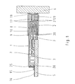
- 1 and 2 is a connector, consisting of a connector 1 and a mating connector 2 shown.
- FIG. 1 shows that applied to a printed circuit board 5 Connector 1 with its protruding electrical spring contacts 20 inside the insulating case 3 in rows and Columns are arranged.
- the contact with the mating connector 2 takes place via the knife contacts 21, which are guided in bushings 23 within the insulating housing 4 and enable the electrical signal connection to a printed circuit board 6.
- the shielding plate 7 on the upper and lower side of the connector 1 is connected to conductor tracks 16 of the printed circuit board 5 by means of contact tabs 15, shown here in a resilient manner, the shielding plate 7 being locked in the channel 25 with the insulating body 3.
- the shielding plates 8 of the mating connector 2 are connected by means of pin-shaped shielding contacts 17, which are guided through openings 18 in the insulating body 4, via conductor tracks 19 to the ground potential of the printed circuit board 6.
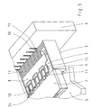
- Fig. 2 are the two connectors in a perspective view 1 and 2 shown in a position just before plugging together. It can be seen that the shielding plates 8 of the mating connector 2, arranged within the outer boundary of the insulating body 4 - above and below are while the knife contacts 23 for electrical signal transmission arranged in rows and columns, inserted in between are. (see also Fig. 1)
- rectangular recesses 22 are provided, in which the flat fastening hooks 24 for the shielding plate 7 of the connector 1 when plugging the two connectors together so that a seamless surface transition between the two connectors is achieved becomes.
- the shielding plate 7 during its assembly, first with its contact tongues 9 in inserted the front flat fastening hooks 24 of the connector 1 and then with locking tabs 13 in corresponding recesses 14 locked in the insulating housing 3 of the connector 1. Doing so simultaneously the shielding plate 7 with its rear end part bent by 90 ° 26 in a correspondingly shaped groove 25 in the insulating housing 3 of Inserted connector 1 and there by means of not shown locking elements locked. This is an electrical connection via the spring here trained contact tabs 15 which on the conductor tracks 16 of the Press circuit board 5, ensured.
- the two plug connectors are connected to one another, so the shielding plates 7 and 8 of the two connectors 1 and 2 contacted each other by the Contact tongues 9 and 10 side by side on one level in each mutually provided gaps so that the ring-shaped trained contact tongues 9 and 10 on the lateral contact surfaces 11 and touch 12.
- the oval rings shown in the example are used slightly compressed and result in a safe electrical contact.
Landscapes
- Details Of Connecting Devices For Male And Female Coupling (AREA)
- Multi-Conductor Connections (AREA)
Applications Claiming Priority (2)
| Application Number | Priority Date | Filing Date | Title |
|---|---|---|---|
| DE19907635 | 1999-02-23 | ||
| DE19907635A DE19907635C1 (de) | 1999-02-23 | 1999-02-23 | Abgeschirmte elektrische Steckverbindung |
Publications (2)
| Publication Number | Publication Date |
|---|---|
| EP1032088A1 true EP1032088A1 (fr) | 2000-08-30 |
| EP1032088B1 EP1032088B1 (fr) | 2001-10-31 |
Family
ID=7898476
Family Applications (1)
| Application Number | Title | Priority Date | Filing Date |
|---|---|---|---|
| EP00101995A Expired - Lifetime EP1032088B1 (fr) | 1999-02-23 | 2000-02-02 | Connecteur électrique blindé |
Country Status (4)
| Country | Link |
|---|---|
| US (1) | US6196875B1 (fr) |
| EP (1) | EP1032088B1 (fr) |
| DE (2) | DE19907635C1 (fr) |
| ES (1) | ES2165834T3 (fr) |
Families Citing this family (2)
| Publication number | Priority date | Publication date | Assignee | Title |
|---|---|---|---|---|
| DE10119695B4 (de) * | 2001-04-20 | 2006-04-13 | Erni Elektroapparate Gmbh | Steckverbinder für elektronische Bauelemente |
| DE102005059990B4 (de) * | 2005-12-13 | 2008-03-20 | Erni Electronics Gmbh | Steckverbinder zur Verbindung elektronischer Bauelemente |
Citations (3)
| Publication number | Priority date | Publication date | Assignee | Title |
|---|---|---|---|---|
| EP0637858A1 (fr) * | 1993-08-06 | 1995-02-08 | Siemens Aktiengesellschaft | Connecteur pour cartes de circuits à deux réglettes de contacts blindées perpendiculaires entre eux |
| DE19508409C1 (de) * | 1995-03-09 | 1996-05-09 | Harting Elektronik Gmbh | Steckverbinder mit Befestigungsmitteln |
| WO1998009354A1 (fr) * | 1996-08-30 | 1998-03-05 | The Whitaker Corporation | Connecteur a plan de masse et d'alimentation |
Family Cites Families (3)
| Publication number | Priority date | Publication date | Assignee | Title |
|---|---|---|---|---|
| NL9200119A (nl) * | 1992-01-22 | 1993-08-16 | Du Pont Nederland | Connector met plaatvormige, interne afscherming. |
| FR2747516B1 (fr) | 1996-04-12 | 1998-06-05 | Framatome Connectors France | Connecteur blinde, notamment du type comprenant une fiche et une embase destinee a etre fixee a un support plan |
| TW371526U (en) * | 1998-06-06 | 1999-10-01 | Hon Hai Prec Ind Co Ltd | Electrical connector |
-
1999
- 1999-02-23 DE DE19907635A patent/DE19907635C1/de not_active Expired - Fee Related
-
2000
- 2000-01-28 US US09/493,972 patent/US6196875B1/en not_active Expired - Lifetime
- 2000-02-02 EP EP00101995A patent/EP1032088B1/fr not_active Expired - Lifetime
- 2000-02-02 ES ES00101995T patent/ES2165834T3/es not_active Expired - Lifetime
- 2000-02-02 DE DE50000023T patent/DE50000023D1/de not_active Expired - Lifetime
Patent Citations (3)
| Publication number | Priority date | Publication date | Assignee | Title |
|---|---|---|---|---|
| EP0637858A1 (fr) * | 1993-08-06 | 1995-02-08 | Siemens Aktiengesellschaft | Connecteur pour cartes de circuits à deux réglettes de contacts blindées perpendiculaires entre eux |
| DE19508409C1 (de) * | 1995-03-09 | 1996-05-09 | Harting Elektronik Gmbh | Steckverbinder mit Befestigungsmitteln |
| WO1998009354A1 (fr) * | 1996-08-30 | 1998-03-05 | The Whitaker Corporation | Connecteur a plan de masse et d'alimentation |
Also Published As
| Publication number | Publication date |
|---|---|
| DE50000023D1 (de) | 2001-12-06 |
| DE19907635C1 (de) | 2000-09-07 |
| EP1032088B1 (fr) | 2001-10-31 |
| US6196875B1 (en) | 2001-03-06 |
| ES2165834T3 (es) | 2002-04-01 |
Similar Documents
| Publication | Publication Date | Title |
|---|---|---|
| DE69506878T2 (de) | Verbesserte erdabdeckung für elektrische verbinder | |
| DE69409831T2 (de) | Koaxialverbinder mit impedanzsteuerung | |
| DE68921165T2 (de) | Abgeschirmte Steckbuchse mit niedrigem Profil. | |
| DE60314228T2 (de) | Verbinderanordnung für l-förmige erdungsabschirmungen und differentialkontaktpaare | |
| DE69103652T3 (de) | Verbinderanordnung für gedruckte Leiterplatten. | |
| DE69520905T2 (de) | Auf einer Oberfläche montierbarer Kartenrandverbinder | |
| DE10063994B4 (de) | Elektronische Komponente, Koaxialverbinder und Kommunikationsvorrichtung | |
| EP0862243B1 (fr) | Connecteur à fiches coaxial à haute fréquence | |
| DE60036250T2 (de) | Modularer Jack-Verbinder mit Filtereinsatz und Kontakt dafür | |
| EP3216088B1 (fr) | Ensemble carte de circuit imprimé | |
| DE10310502A1 (de) | Elektrischer Verbinder mit Erdungsanschluss | |
| EP1251591B1 (fr) | Connecteur pour des composants électroniques | |
| DE69803920T2 (de) | Koaxialverbinder für gedruckte schaltungen | |
| DE102012105256A1 (de) | Isolierkörper eines Steckverbinders | |
| DE102012105257B4 (de) | Isolierkörper eines Steckverbinders | |
| EP1083630B1 (fr) | Connecteur coaxial à fiche | |
| DE4000407A1 (de) | Elektrische steckverbindung | |
| DE202007002248U1 (de) | Kodiereinrichtung für Steckverbinder | |
| DE69420144T2 (de) | Elektrisches Stiftfeld auf einer Leiterplatte | |
| EP2037541A2 (fr) | Connecteur à fiche doté d'une platine | |
| WO2020021091A1 (fr) | Connecteur de bord enfichable et ensemble de carte de circuit imprimé | |
| EP1032088B1 (fr) | Connecteur électrique blindé | |
| DE10029925C1 (de) | Leiterplattensteckverbindung | |
| DE69927662T2 (de) | Verbinder zum Abschliessen von Fernmeldekabeln | |
| EP0658955A2 (fr) | Filtre plan pour un connecteur à plusieurs pôles |
Legal Events
| Date | Code | Title | Description |
|---|---|---|---|
| PUAI | Public reference made under article 153(3) epc to a published international application that has entered the european phase |
Free format text: ORIGINAL CODE: 0009012 |
|
| AK | Designated contracting states |
Kind code of ref document: A1 Designated state(s): DE ES FI FR GB SE |
|
| AX | Request for extension of the european patent |
Free format text: AL;LT;LV;MK;RO;SI |
|
| 17P | Request for examination filed |
Effective date: 20001016 |
|
| GRAG | Despatch of communication of intention to grant |
Free format text: ORIGINAL CODE: EPIDOS AGRA |
|
| GRAG | Despatch of communication of intention to grant |
Free format text: ORIGINAL CODE: EPIDOS AGRA |
|
| GRAH | Despatch of communication of intention to grant a patent |
Free format text: ORIGINAL CODE: EPIDOS IGRA |
|
| 17Q | First examination report despatched |
Effective date: 20010125 |
|
| AKX | Designation fees paid |
Free format text: DE ES FI FR GB SE |
|
| GRAH | Despatch of communication of intention to grant a patent |
Free format text: ORIGINAL CODE: EPIDOS IGRA |
|
| GRAA | (expected) grant |
Free format text: ORIGINAL CODE: 0009210 |
|
| AK | Designated contracting states |
Kind code of ref document: B1 Designated state(s): DE ES FI FR GB SE |
|
| REF | Corresponds to: |
Ref document number: 50000023 Country of ref document: DE Date of ref document: 20011206 |
|
| REG | Reference to a national code |
Ref country code: GB Ref legal event code: IF02 |
|
| GBT | Gb: translation of ep patent filed (gb section 77(6)(a)/1977) |
Effective date: 20020110 |
|
| REG | Reference to a national code |
Ref country code: ES Ref legal event code: FG2A Ref document number: 2165834 Country of ref document: ES Kind code of ref document: T3 |
|
| PG25 | Lapsed in a contracting state [announced via postgrant information from national office to epo] |
Ref country code: FR Free format text: LAPSE BECAUSE OF FAILURE TO SUBMIT A TRANSLATION OF THE DESCRIPTION OR TO PAY THE FEE WITHIN THE PRESCRIBED TIME-LIMIT Effective date: 20020906 |
|
| PLBE | No opposition filed within time limit |
Free format text: ORIGINAL CODE: 0009261 |
|
| STAA | Information on the status of an ep patent application or granted ep patent |
Free format text: STATUS: NO OPPOSITION FILED WITHIN TIME LIMIT |
|
| 26N | No opposition filed | ||
| ET | Fr: translation filed | ||
| EN | Fr: translation not filed |
Free format text: BO 2002/36, PAGES: 179: IL Y A LIEU DE SUPPRIMER: LA MENTION DE LA NON REMISE. LA TRADUCTION EST PUBLIEE DANS LE PRESENT BOPI. |
|
| REG | Reference to a national code |
Ref country code: GB Ref legal event code: 732E |
|
| REG | Reference to a national code |
Ref country code: FR Ref legal event code: TP |
|
| REG | Reference to a national code |
Ref country code: ES Ref legal event code: PC2A |
|
| PGFP | Annual fee paid to national office [announced via postgrant information from national office to epo] |
Ref country code: FI Payment date: 20120221 Year of fee payment: 13 Ref country code: SE Payment date: 20120221 Year of fee payment: 13 Ref country code: GB Payment date: 20120221 Year of fee payment: 13 |
|
| PGFP | Annual fee paid to national office [announced via postgrant information from national office to epo] |
Ref country code: ES Payment date: 20120213 Year of fee payment: 13 |
|
| REG | Reference to a national code |
Ref country code: SE Ref legal event code: EUG |
|
| GBPC | Gb: european patent ceased through non-payment of renewal fee |
Effective date: 20130202 |
|
| PG25 | Lapsed in a contracting state [announced via postgrant information from national office to epo] |
Ref country code: FI Free format text: LAPSE BECAUSE OF NON-PAYMENT OF DUE FEES Effective date: 20130202 Ref country code: SE Free format text: LAPSE BECAUSE OF NON-PAYMENT OF DUE FEES Effective date: 20130203 |
|
| PG25 | Lapsed in a contracting state [announced via postgrant information from national office to epo] |
Ref country code: GB Free format text: LAPSE BECAUSE OF NON-PAYMENT OF DUE FEES Effective date: 20130202 |
|
| REG | Reference to a national code |
Ref country code: ES Ref legal event code: FD2A Effective date: 20140409 |
|
| PG25 | Lapsed in a contracting state [announced via postgrant information from national office to epo] |
Ref country code: ES Free format text: LAPSE BECAUSE OF NON-PAYMENT OF DUE FEES Effective date: 20130203 |
|
| REG | Reference to a national code |
Ref country code: FR Ref legal event code: PLFP Year of fee payment: 17 |
|
| PGFP | Annual fee paid to national office [announced via postgrant information from national office to epo] |
Ref country code: DE Payment date: 20160127 Year of fee payment: 17 |
|
| PGFP | Annual fee paid to national office [announced via postgrant information from national office to epo] |
Ref country code: FR Payment date: 20160108 Year of fee payment: 17 |
|
| REG | Reference to a national code |
Ref country code: DE Ref legal event code: R119 Ref document number: 50000023 Country of ref document: DE |
|
| REG | Reference to a national code |
Ref country code: FR Ref legal event code: ST Effective date: 20171031 |
|
| PG25 | Lapsed in a contracting state [announced via postgrant information from national office to epo] |
Ref country code: FR Free format text: LAPSE BECAUSE OF FAILURE TO SUBMIT A TRANSLATION OF THE DESCRIPTION OR TO PAY THE FEE WITHIN THE PRESCRIBED TIME-LIMIT Effective date: 20170228 Ref country code: DE Free format text: LAPSE BECAUSE OF NON-PAYMENT OF DUE FEES Effective date: 20170901 |