EP1031994B1 - Speicherschaltungen mit eingebautem Selbsttest - Google Patents
Speicherschaltungen mit eingebautem Selbsttest Download PDFInfo
- Publication number
- EP1031994B1 EP1031994B1 EP99103478A EP99103478A EP1031994B1 EP 1031994 B1 EP1031994 B1 EP 1031994B1 EP 99103478 A EP99103478 A EP 99103478A EP 99103478 A EP99103478 A EP 99103478A EP 1031994 B1 EP1031994 B1 EP 1031994B1
- Authority
- EP
- European Patent Office
- Prior art keywords
- test
- memory
- memory device
- macro
- dram
- Prior art date
- Legal status (The legal status is an assumption and is not a legal conclusion. Google has not performed a legal analysis and makes no representation as to the accuracy of the status listed.)
- Expired - Lifetime
Links
- 238000012360 testing method Methods 0.000 title claims abstract description 106
- 230000015654 memory Effects 0.000 title claims description 53
- 238000000034 method Methods 0.000 claims abstract description 28
- 230000004044 response Effects 0.000 claims description 32
- 230000006870 function Effects 0.000 claims description 4
- 230000007246 mechanism Effects 0.000 claims description 3
- 238000013461 design Methods 0.000 abstract description 7
- 230000015572 biosynthetic process Effects 0.000 abstract description 3
- 230000008569 process Effects 0.000 abstract description 3
- 238000003786 synthesis reaction Methods 0.000 abstract description 3
- 238000005516 engineering process Methods 0.000 abstract description 2
- 230000007704 transition Effects 0.000 description 7
- 230000009471 action Effects 0.000 description 4
- 238000013459 approach Methods 0.000 description 2
- 230000015556 catabolic process Effects 0.000 description 2
- 238000004891 communication Methods 0.000 description 2
- 238000006731 degradation reaction Methods 0.000 description 2
- 238000010586 diagram Methods 0.000 description 2
- 238000012986 modification Methods 0.000 description 2
- 230000004048 modification Effects 0.000 description 2
- 230000001360 synchronised effect Effects 0.000 description 2
- 238000004458 analytical method Methods 0.000 description 1
- 230000007547 defect Effects 0.000 description 1
- 230000001934 delay Effects 0.000 description 1
- 230000009977 dual effect Effects 0.000 description 1
- 239000000428 dust Substances 0.000 description 1
- 230000000694 effects Effects 0.000 description 1
- 238000011990 functional testing Methods 0.000 description 1
- 238000004519 manufacturing process Methods 0.000 description 1
- 238000005457 optimization Methods 0.000 description 1
- 239000002245 particle Substances 0.000 description 1
- 238000012545 processing Methods 0.000 description 1
- 230000003068 static effect Effects 0.000 description 1
- 238000012546 transfer Methods 0.000 description 1
- 238000013519 translation Methods 0.000 description 1
Images
Classifications
-
- G—PHYSICS
- G11—INFORMATION STORAGE
- G11C—STATIC STORES
- G11C29/00—Checking stores for correct operation ; Subsequent repair; Testing stores during standby or offline operation
- G11C29/04—Detection or location of defective memory elements, e.g. cell constructio details, timing of test signals
- G11C29/08—Functional testing, e.g. testing during refresh, power-on self testing [POST] or distributed testing
- G11C29/12—Built-in arrangements for testing, e.g. built-in self testing [BIST] or interconnection details
- G11C29/14—Implementation of control logic, e.g. test mode decoders
- G11C29/16—Implementation of control logic, e.g. test mode decoders using microprogrammed units, e.g. state machines
Definitions
- the invention relates to a test and a test hardware of a memory. More particularly, the invention relates to a built-in self-test circuit for memories embedded on the same chip.
- Memories are susceptible to fabrication process related failures caused by dust particles on the chips or masks, scratches and gate oxide pinholes, which may result open or short circuits. Many methods or hardwares have been developed to test whether a memory can function normally. However, as the integrated circuit art becomes more and more advanced, functions of memories become much more and more complex. Consequently, it often takes a great time and requires a complex circuit to perform a functional test of the memories.
- BIST built-in self-test
- a test algorithm is translated into a sequence of commands, data, and addresses applied to the memory under test.
- FSM hard-wired finite state machine
- the BIST circuit operates as fast as the memory under test.
- a disadvantage of the approach is that the finite state machine is tailored to a specific set of test patterns whose complexity depends on the test algorithm. As the complexity of the test algorithm increases, this approach may be inadequate because the finite state machine may become too large and too slow to produce a test pattern in each clock cycle to intensively exercise the memory under test.
- Some BIST circuits known to be the programmable or configurable BIST circuits, can be referred to U.S. Patent No. 5,173,906, "Built-in Self-Test for Integrated Circuit” disclosed by Dreibelbis et al, in 1992.
- Another disclosure of a circuit that uses a micro-coded sequence defined in the contents of a read-only memory to produce the test patterns is issued with a US Patent No. 5,224,101 to Popyack et al in 1993.
- US Patent No. 5,224,101 to Popyack et al in 1993.
- the test algorithm for a dynamic random access memory (DRAM) is typically complex and requires a relatively long period of time to perform the test.
- DRAM dynamic random access memory
- the invention provides a circuit for memory testing, especially for a DRAM.
- the circuit comprises two finite state machines, so as to adapt the pipeline technique.
- a certain protocol on communicating these two finite machines is established.
- the timing criticality of the design is further relaxed.
- the invention provides a built-in self-test circuit for testing a memory embedded on the same chip, especially for testing a DRAM.
- the built-in circuit comprises two finite state machines, a queue, an encoder, a memory input buffer, a delay buffer, and a comparator in a pipeline structure.
- One of the finite state machines is called a producer which translates a test algorithm into a sequence of macro-instructions.
- the other finite state machine is called a scheduler which further interprets each of these macro-instructions into a series of test patterns.
- the queue is connected between the producer and the scheduler serving as a synchronization buffer, so that an operation of "latch-and-shift forward" is performed.
- the test patterns are then input from the scheduler to the encoder which encodes the test patterns from one-hot code into a binary code defined by the memory.
- the pipeline thus comprises three stages, the first stage translates the test algorithm into the macro-instructions, the second stage interprets the macro-instructions into the test patterns, and the third stage encodes the one-hot code into the memory defined binary code. Due to the potential performance degradation of the memory device introduced by the BIST circuit, the encoder is further connected to a BIST output buffer (BOB).
- BOB BIST output buffer
- the delay buffer is connected between the BIST output buffer and the comparator. An expected response of memory is computed thereby.
- the delay buffer outputs the computed result of the expected response to the comparator.
- the comparator then compares the expected response with the memory test response to determine whether the memory fails or passes.
- the invention further provides a method for testing a memory, especially for testing a DRAM.
- a test algorithm is input and translated by a first finite machine into a sequence of macro-instructions. Being synchronized by a queue according to a communication protocol, each of the macro-instructions is interpreted into a sequence of one-hot encoded test patterns. Each of the one-hot encoded test patterns is then mapped to a code defined by the DRAM. Via the BIST delay buffer, the mapped codes are fed into the DRAM to perform a test.
- a multiplexer MUX is further installed between the BIST circuit and the DRAM.
- the test results of both the output response of the DRAM and an expected memory response are input to the comparator
- the comparator compares the output response of the DRAM with the expected memory response While the test response of the memory appears the same as the expected response, the BIST circuit displays a "pass" information. On the contrary, if the test response of the memory is different from the expected response, the BIST circuit indicates a fail information.
- a test algorithm written as a program in a high-level language is often proposed.
- a test algorithm written as a program in a high-level language.
- four steps are included in a march algorithm.
- a first step '0' is written to every cell.
- the second step walks through the entire array in a forward manner, that is, from the first cell in the first row to the last cell in the last row.
- a so-called READ(0)-WRITE(1)-READ(1) operation is performed.
- This READ-WRITE-READ operation is proposed in an attempt to better expose the potential dynamic defects of the memory cells.
- the third step walks through the entire cell from the last cell to the first cell. At each cell, a READ(1)-WRITE(0)-READ(0) operation is performed.
- the fourth step of this algorithm checks if the value of every cell is still zero after the first three steps.
- a pipeline comprising three stages for translating the high-level algorithm into test patterns for a memory device to be tested by a BIST circuit.
- the algorithm is first translated into a sequence of macro-instructions in the first stage, followed by further interpreting each of the macro-instructions into a sequence of test patterns in the second stage.
- the one-hot codes of the test patterns are then encoded into a binary code defined by the memory device.
- a DRAM is taken as an example to be tested.
- a basic activity often comprises at least one of the memory commands ⁇ mem_nop, mem_active, mem_read, mem_write , mem_precharge , mem_refresh ⁇ defined by the DRAM, where
- a READ operation to a memory cell may be composed of the sequence of ⁇ mem_active ⁇ mem_nop ⁇ mem_read ⁇ mem_read ⁇ mem_nop ⁇ mem_precharge ⁇ .
- a test pattern further comprises data value, row address, and column address.
- the macro-instructions are expressed by four-tuples (opcode, data, row-address, column-address), where data, row address, and column address could be "Don't care” represented by "*”. Seven types of macro-instructions are used in the design:
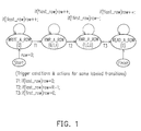
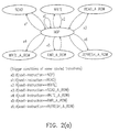
- Fig. 1, Fig.2(a) and Fig. 2(b) respectively show the state transition graphs of the two finite machines for implementing the marching algorithm. Both machines operate along with an incrementer that keeps track of the row address and/or column address (represented by variables row and col ).
- the first machine comprises four symbolic states excluding the start and finish states as shown in Fig. 1. Each transition may associate a trigger condition and an operation.
- the trigger condition is the condition that needs to be satisfied in order to exercise the associated transition, while the operation is the action to be taken with the transition.
- the second machine as shown in Fig. 2(a) and Fig. 2(b), taking the macro-instructions generated by the first machine as input, is a hierarchical state machine with seven sub-machines. Each sub-machine is used to interpret one type of macro-instruction. For simplicity, only the three sub-machines needed for the march algorithm described above is shown (that is, READ_A_ROW, WRITE_A_ROW, and RWR_A_ROW) In a more sophisticated test algorithm of a DRAM, for example. the commonly used row disturb algorithm, may need all macro-instructions.
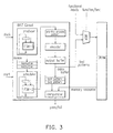
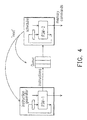
- Fig. 3 shows a block diagram of a built-in self-test circuit for testing a memory according to a preferred embodiment of the invention.
- This built-in self-test circuit is particularly applicable for testing a memory requiring a complex test algorithm, for example, for testing a dynamic random access memory.
- the main objective of the BIST circuit is to translate a number of high-level abstract algorithms into a sequence of test patterns.
- the BIST circuitry needs to operate at least as fast as the memory device under test.
- the single finite state machine may become too large, and thus too slow to produce a test pattern for every clock cycle when applied to high-speed memory devices. Therefore, a pipeline technique is employed and a high-speed BIST architecture comprising dual finite state machines is provided in the invention.
- the BIST circuit comprises a first finite state machine, namely, a producer, a queue, a second finite state machine, also called a scheduler, an encoder, an (BIST) output buffer (BOB), a delay buffer, and a comparator.
- a pipeline technique is employed to construct the BIST circuit. There are three stages in this pipeline design, that is, a macro-instruction generation via the producer in the first stage, a macro-instruction scheduling via the scheduler in the second stage, and a memory command encoding via the encoder in the third stage. Between the producer and the scheduler, a communicating protocol is established and will be described as follows.
- test algorithm While the producer receives a high-level test algorithm, the test algorithm is translated into a sequence of macro-instructions thereby. This is the first stage of a pipeline.
- the second finite machine interprets each macro-instruction into a sequence of test patterns, in which memory command parts are one-hot encoded. This component, related to the interface with the memory device, forms the second stage of the pipeline.
- the queue is preferably a first-in-first-out register, serving as a synchronization buffer connected between the first and the second finite machines.
- the producer is capable of producing one macro-instruction every cycle.
- the scheduler can take multiple clock cycles to complete the processing of a macro-instruction. Therefore, the producer may have to be stalled from time to time in order to avoid overloading the scheduler with excessive macro-instructions.
- a simple master-slave synchronization mechanism wherein the scheduler is the master which controls the action of the producer and the synchrontzation queue through a signal named ' next ',
- the scheduler is the master which controls the action of the producer and the synchrontzation queue through a signal named ' next '
- the producer and the queue are frozen, that is, the value of every flip-flop of the queue remains unchanged regardless of the clocking.
- the signal ' next ' is raised to high, the current macro-instruction produced by the producer is inserted to the queue at the specified clock edge. Meanwhile, the producer enters the next state to compute the next macro-instruction.
- the queue when the signal ' next ' is asserted, the queue performs a shift-forward operation and latches in a new instruction generated by the producer at the same clock cycle. On the other hand, if the signal ' next ' is de-asserted, the queue performs no operation. Thus, the only operation associated with this queue is " latch-and-shift-forward ".
- the encoder is a piece of combinational logic that maps the encoding of each memory command in the test patterns output by the scheduler from one-hot to the one defined by the memory device. For example, if an input vector of the input test pattern is (00001, 0, 0, 0), where "00001" represents the one-hot code of a read memory command. Being processed by the encoder, this read memory command is encoded into a binary code of a read memory command defined by the memory device to be tested by the BIST circuit.
- the BIST output buffer is a register that serves as a buffer between the BIST circuit and the memory device. This buffer eliminates the potential performance degradation of the memory device due to the introduction of the BIST circuit.
- the delay buffer again, is a first-in-first-out register file between the BIST output buffer and the comparator It is primarily for computing the expected responses of the read memory command.
- the number of clock cycle delays from BIST output buffer to the comparator corresponds to the CAS-latency defined by the memory device.
- the comparator is a piece of combinational logic that compares the output responses of the memory device with the expected values provided by the delay buffer. For example, if a test pattern ( mem_read , 1, 0, 0) is applied to the memory device and the CAS-latency is two, then two clock cycles later, the memory device is supposed to produce a '1' at the data output. Meanwhile, the same test pattern should arrive at the comparator through the delay buffer and the data part '1' of the test pattern ( mem _ read , 1, 0, 0), can be extracted as the expected value for the comparison.
- a technique called protocol-based relaxation to boost the BIST circuit speed is further proposed.
- This technique is based on an observation that, among the three stages, the timing critical paths are mostly the producer.
- the producer is transformed into a multi-cycle path component (that is, a component produces one result for every two clock cycles or more). Since scheduler controls the action of the producer, this can be achieved by modifying the scheduler. The modification needs to be done in such a way that the signal ' next ' will not be raised to high for two consecutive clock cycles.
- the method and the BIST circuit for testing a memory device can thus be briefly summarized as follows. While a test algorithm is input to the producer, the test algorithm is translated into a sequence of macro-instructions. Being synchronized by a queue according to a communication protocol, each of the macro-instructions is interpreted into a sequence of one-hot encoded test patterns. Each of the one-hot encoded test patterns is then mapped to a code defined by the DRAM. Via the BIST delay buffer, the mapped codes are fed into the DRAM for performing a test. As shown in the figure, a multiplexer (MUX) is further installed between the BIST circuit and the DRAM.
- MUX multiplexer
- the test result that is, the output response of the DRAM is then input to the comparator, so does an expected memory response.
- the comparator compares the output response of the DRAM with the expected memory response. While the test response of the memory appears the same as the expected response, the BIST circuit displays a "pass" information. On the contrary, if the test response of the memory is different from the expected response, the BIST circuit indicates a fail information.
- the present invention has been implemented as a register transfer level (RTL) code. It is simulated with the functional model of the memory device under test to establish the confidence of its functional correctness. Synthesis tool, design compile, is used to convert this RTL code into a netlist and perform logic optimization using 0.25 ⁇ m CMOS technology library. Static timing analysis tool, design time, shows theat the clock cycle time is under 2.21ns. The timing-driven feature of a place-and-rout tool, Apollo, is used generate the layout. Post-layout timing check shows no timing violation under above clock cycle time. Based on these results, we thus can conclude the proposed BIST architecture in the invention has great potential to run as fast as 450MHz.
- RTL register transfer level
Landscapes
- Tests Of Electronic Circuits (AREA)
- For Increasing The Reliability Of Semiconductor Memories (AREA)
Claims (12)
- Integrierter Selbsttest-Schaltkreis (BIST) für einen dynamischen Direktzugriffsspeicher (DRAM), welcher aufweist:einen ersten endlichen Automaten zum Übersetzen eines Eingabe-Test-Algorithmus in eine Sequenz von Makro-Anweisungen;einen zweiten endlichen Automaten, zum Interpretieren jeder der Makro-Anweisungen in eine Sequenz von one-hot kodierten Testmustern;ein first-in-first-out Register, das als Synchronisations-Puffer zwischen dem ersten endlichen Automaten und dem zweiten endlichen Automaten dient; einen Kodierer, zum Kodieren von one-hot Kodes der Testmuster in Binärkodes, welche mittels des DRAMs definiert sind;einen BIST Ausgangspuffer, der als Puffer für die Binärkodes dient, welche dann zum Ausführen eines Tests in den DRAM eingegeben werden;einen Verzögerungspuffer zum Verzögern einer erwarteten DRAM-Antwort gemäß den one-hot kodierten Testmustern; undeinen Komparator zum Vergleichen einer Ausgangsantwort des DRAMs mit der erwarteten Antwort des DRAMs, welche von dem Verzögerungspuffer bereitgestellt wird, um so zu entscheiden, ob die Speichereinheit korrekt funktioniert.
- Verknüpfungsstruktur gemäß Anspruch 1, wobei die Sequenz an Makro-Anweisungen gemäß einer Sequenz von Speicherbefehlen definiert ist, welche mittels des DRAMs definiert ist.
- Integrierter Selbsttest-Schaltkreis gemäß Anspruch 1, welcher weiterhin einen Multiplexer zwischen dem integrierten Selbsttest-Schaltkreis und dem DRAM aufweist.
- Integrierter Selbsttest-Schaltkreis gemäß Anspruch 1, wobei der Verzögerungspuffer ein first-in-first-out Register aufweist.
- Verfahren zum Testen einer Speichereinrichtung, unter Verwendung eines integrierten Selbsttest-Schaltkreises, wobei das Verfahren aufweist:Übersetzen eines Test-Algorithmus in eine Sequenz von Makro-Anweisungen gemäß einer Mehrzahl von Speicherbefehlen, welche mittels der Speichereinrichtung definiert werden;Übersetzen jeder der Makro-Anweisungen in eine Sequenz von one-hot kodierten Testmuster, welche Daten, eine Adresse und Befehle aufweisen;Kodieren einer Mehrzahl von one-hot Kodes der Testmuster in Binärkodes, welche mittels der Speichereinrichtung definiert werden, um auf der Speichereinrichtung einen Test durchzuführen;Verzögern einer erwarteten Speicherantwort gemäß einer mittels der Speichereinrichtung definierten CAS-Latenzzeit; undVergleichen der erwarteten Speicher-Antwort mit einer Ausgabe-Antwort der Speichereinrichtung, nachdem sie, um zu entscheiden, ob die Speichereinrichtung normal funktioniert, getestet wurde.
- Verfahren gemäß Anspruch 5, wobei ein Generator verwendet wird, um die Sequenz von Makro-Anweisungen zu erzeugen.
- Verfahren gemäß Anspruch 6, wobei ein Scheduler verwendet wird, um jede der Makro-Anweisungen in die Sequenz von Testmustern zu übersetzen.
- Verfahren gemäß Anspruch 7, wobei eine Warteschlange implementiert ist, um den Generator und den Scheduler in Verbindung zu bringen, wobei ein Synchronisations-Master-Slave Mechanismus verwendet wird.
- Verfahren gemäß Anspruch 8, wobei der Scheduler als Master zum Steuern der Warteschlange und der Generator als Slave funktionieren.
- Verfahren gemäß Anspruch 6, wobei der Generator, der Scheduler und ein Koder, welcher die Kodierschritte durchführt, eine dreistufige Pipeline bilden.
- Verfahren gemäß Anspruch 5, wobei die Speichereinrichtung einen dynamischen Direktzugriffsspeicher aufweist.
- Verfahren gemäß Anspruch 5, wobei die Speichereinrichtung versagt, wenn die erwartete Speicher-Antwort die gleiche ist wie die Ausgangs-Antwort der Speichereinrichtung, nachdem die Speichereinrichtung getestet wurde, während die Speichereinrichtung besteht, wenn die erwartete Speicher-Antwort von der Ausgangs-Antwort der Speichereinrichtung abweicht.
Priority Applications (3)
| Application Number | Priority Date | Filing Date | Title |
|---|---|---|---|
| DE69902221T DE69902221T2 (de) | 1999-02-23 | 1999-02-23 | Speicherschaltungen mit eingebautem Selbsttest |
| EP99103478A EP1031994B1 (de) | 1999-02-23 | 1999-02-23 | Speicherschaltungen mit eingebautem Selbsttest |
| US09/290,384 US6351837B1 (en) | 1999-02-23 | 1999-04-12 | High speed built-in self-test circuit for DRAMS |
Applications Claiming Priority (1)
| Application Number | Priority Date | Filing Date | Title |
|---|---|---|---|
| EP99103478A EP1031994B1 (de) | 1999-02-23 | 1999-02-23 | Speicherschaltungen mit eingebautem Selbsttest |
Publications (2)
| Publication Number | Publication Date |
|---|---|
| EP1031994A1 EP1031994A1 (de) | 2000-08-30 |
| EP1031994B1 true EP1031994B1 (de) | 2002-07-24 |
Family
ID=8237618
Family Applications (1)
| Application Number | Title | Priority Date | Filing Date |
|---|---|---|---|
| EP99103478A Expired - Lifetime EP1031994B1 (de) | 1999-02-23 | 1999-02-23 | Speicherschaltungen mit eingebautem Selbsttest |
Country Status (3)
| Country | Link |
|---|---|
| US (1) | US6351837B1 (de) |
| EP (1) | EP1031994B1 (de) |
| DE (1) | DE69902221T2 (de) |
Families Citing this family (14)
| Publication number | Priority date | Publication date | Assignee | Title |
|---|---|---|---|---|
| US7770016B2 (en) * | 1999-07-29 | 2010-08-03 | Intertrust Technologies Corporation | Systems and methods for watermarking software and other media |
| US7430670B1 (en) | 1999-07-29 | 2008-09-30 | Intertrust Technologies Corp. | Software self-defense systems and methods |
| US6829728B2 (en) * | 2000-11-13 | 2004-12-07 | Wu-Tung Cheng | Full-speed BIST controller for testing embedded synchronous memories |
| US6650592B2 (en) * | 2001-11-29 | 2003-11-18 | International Business Machines Corporation | Data processing system, method, and product for automatically performing timing checks on a memory cell using a static timing tool |
| US6879530B2 (en) | 2002-07-18 | 2005-04-12 | Micron Technology, Inc. | Apparatus for dynamically repairing a semiconductor memory |
| US7017094B2 (en) | 2002-11-26 | 2006-03-21 | International Business Machines Corporation | Performance built-in self test system for a device and a method of use |
| US7734966B1 (en) | 2002-12-26 | 2010-06-08 | Marvell International Ltd. | Method and system for memory testing and test data reporting during memory testing |
| JP2006252267A (ja) * | 2005-03-11 | 2006-09-21 | Oki Electric Ind Co Ltd | システム検証用回路 |
| US20070050668A1 (en) * | 2005-09-01 | 2007-03-01 | Micron Technology, Inc. | Test mode to force generation of all possible correction codes in an ECC memory |
| EP2186028A2 (de) * | 2007-08-07 | 2010-05-19 | Nxp B.V. | Einrichtung und verfahren zur modellierung einer physischen struktur |
| US8726114B1 (en) * | 2012-11-09 | 2014-05-13 | Oracle International Corporation | Testing of SRAMS |
| US20160132317A1 (en) | 2014-11-06 | 2016-05-12 | Intertrust Technologies Corporation | Secure Application Distribution Systems and Methods |
| KR102817444B1 (ko) * | 2020-02-11 | 2025-06-05 | 삼성전자주식회사 | 메모리 테스트 장치 및 테스트 방법 |
| CN115389911B (zh) * | 2022-08-25 | 2023-04-14 | 北京物芯科技有限责任公司 | 芯片调度器故障判断方法、装置、电子设备及存储介质 |
Family Cites Families (13)
| Publication number | Priority date | Publication date | Assignee | Title |
|---|---|---|---|---|
| US3831148A (en) * | 1973-01-02 | 1974-08-20 | Honeywell Inf Systems | Nonexecute test apparatus |
| IT1047437B (it) | 1975-10-08 | 1980-09-10 | Cselt Centro Studi Lab Telecom | Procedimento e dispositivo per il controllo in linea di memorie logiche sequenziali operanti a divisione di tempo |
| US5329471A (en) * | 1987-06-02 | 1994-07-12 | Texas Instruments Incorporated | Emulation devices, systems and methods utilizing state machines |
| US5557619A (en) * | 1994-04-04 | 1996-09-17 | International Business Machines Corporation | Integrated circuits with a processor-based array built-in self test circuit |
| KR100191143B1 (ko) | 1994-08-19 | 1999-06-15 | 오우라 히로시 | 고속패턴 발생기 |
| US5742840A (en) * | 1995-08-16 | 1998-04-21 | Microunity Systems Engineering, Inc. | General purpose, multiple precision parallel operation, programmable media processor |
| US5883843A (en) * | 1996-04-30 | 1999-03-16 | Texas Instruments Incorporated | Built-in self-test arrangement for integrated circuit memory devices |
| US6061817A (en) * | 1996-06-10 | 2000-05-09 | Cypress Semiconductor Corp. | Method and apparatus for generating test pattern for sequence detection |
| US5748640A (en) * | 1996-09-12 | 1998-05-05 | Advanced Micro Devices | Technique for incorporating a built-in self-test (BIST) of a DRAM block with existing functional test vectors for a microprocessor |
| US5883905A (en) | 1997-02-18 | 1999-03-16 | Schlumberger Technologies, Inc. | Pattern generator with extended register programming |
| US5961653A (en) * | 1997-02-19 | 1999-10-05 | International Business Machines Corporation | Processor based BIST for an embedded memory |
| US6122760A (en) * | 1998-08-25 | 2000-09-19 | International Business Machines Corporation | Burn in technique for chips containing different types of IC circuitry |
| US6128749A (en) * | 1998-11-03 | 2000-10-03 | Intel Corporation | Cross-clock domain data transfer method and apparatus |
-
1999
- 1999-02-23 EP EP99103478A patent/EP1031994B1/de not_active Expired - Lifetime
- 1999-02-23 DE DE69902221T patent/DE69902221T2/de not_active Expired - Lifetime
- 1999-04-12 US US09/290,384 patent/US6351837B1/en not_active Expired - Lifetime
Also Published As
| Publication number | Publication date |
|---|---|
| US6351837B1 (en) | 2002-02-26 |
| EP1031994A1 (de) | 2000-08-30 |
| DE69902221D1 (de) | 2002-08-29 |
| DE69902221T2 (de) | 2003-03-06 |
Similar Documents
| Publication | Publication Date | Title |
|---|---|---|
| US7721174B2 (en) | Full-speed BIST controller for testing embedded synchronous memories | |
| KR100328357B1 (ko) | 개선된자동메모리테스터용용장성분석기 | |
| KR970004074B1 (ko) | 메모리 장치 및 이를 포함한 집적 회로 | |
| EP1031994B1 (de) | Speicherschaltungen mit eingebautem Selbsttest | |
| US5173906A (en) | Built-in self test for integrated circuits | |
| KR100488232B1 (ko) | 집적 dma 제어기를 이용한 집적 메모리 테스트 방법 | |
| US6510530B1 (en) | At-speed built-in self testing of multi-port compact sRAMs | |
| US20060031725A1 (en) | Algorithm pattern generator for testing a memory device and memory tester using the same | |
| Camurati et al. | Industrial BIST of embedded RAMs | |
| US6687861B1 (en) | Memory tester with enhanced post decode | |
| Cheng et al. | Automatic generation of memory built-in self-test cores for system-on-chip | |
| US6647524B1 (en) | Built-in-self-test circuit for RAMBUS direct RDRAM | |
| Lee et al. | Reduced-pin-count BOST for test-cost reduction | |
| JP3628545B2 (ja) | メモリー素子用内蔵自己テスト回路 | |
| EP1031995B1 (de) | Speicherschaltung mit eingebautem Selbsttest | |
| US8917566B2 (en) | Bypass structure for a memory device and method to reduce unknown test values | |
| JP3667146B2 (ja) | メモリ用内蔵自己テスト回路 | |
| Huang | On speeding up extended finite state machines using catalyst circuitry | |
| Cheng | Comprehensive study on designing memory BIST: algorithms, implementations and trade-offs | |
| Shen et al. | A high speed BIST architecture for DDR-SDRAM testing | |
| KR100683436B1 (ko) | 메모리 자체 테스트 회로 생성기 | |
| Jone et al. | An efficient BIST method for distributed small buffers | |
| Huang et al. | A BIST Architecture For At-Speed DRAM Testing | |
| Huang et al. | A high-speed built-in-self-test design for drams | |
| CA2426040A1 (en) | At-speed built-in self testing of multi-port compact srams |
Legal Events
| Date | Code | Title | Description |
|---|---|---|---|
| PUAI | Public reference made under article 153(3) epc to a published international application that has entered the european phase |
Free format text: ORIGINAL CODE: 0009012 |
|
| AK | Designated contracting states |
Kind code of ref document: A1 Designated state(s): DE FR GB NL |
|
| AX | Request for extension of the european patent |
Free format text: AL;LT;LV;MK;RO;SI |
|
| 17P | Request for examination filed |
Effective date: 20010227 |
|
| AKX | Designation fees paid |
Free format text: DE FR GB NL |
|
| 17Q | First examination report despatched |
Effective date: 20010530 |
|
| GRAG | Despatch of communication of intention to grant |
Free format text: ORIGINAL CODE: EPIDOS AGRA |
|
| GRAG | Despatch of communication of intention to grant |
Free format text: ORIGINAL CODE: EPIDOS AGRA |
|
| GRAH | Despatch of communication of intention to grant a patent |
Free format text: ORIGINAL CODE: EPIDOS IGRA |
|
| GRAH | Despatch of communication of intention to grant a patent |
Free format text: ORIGINAL CODE: EPIDOS IGRA |
|
| GRAA | (expected) grant |
Free format text: ORIGINAL CODE: 0009210 |
|
| AK | Designated contracting states |
Kind code of ref document: B1 Designated state(s): DE FR GB NL |
|
| REG | Reference to a national code |
Ref country code: GB Ref legal event code: FG4D |
|
| REF | Corresponds to: |
Ref document number: 69902221 Country of ref document: DE Date of ref document: 20020829 |
|
| ET | Fr: translation filed | ||
| PLBE | No opposition filed within time limit |
Free format text: ORIGINAL CODE: 0009261 |
|
| STAA | Information on the status of an ep patent application or granted ep patent |
Free format text: STATUS: NO OPPOSITION FILED WITHIN TIME LIMIT |
|
| 26N | No opposition filed |
Effective date: 20030425 |
|
| REG | Reference to a national code |
Ref country code: FR Ref legal event code: PLFP Year of fee payment: 17 |
|
| REG | Reference to a national code |
Ref country code: FR Ref legal event code: PLFP Year of fee payment: 18 |
|
| REG | Reference to a national code |
Ref country code: FR Ref legal event code: PLFP Year of fee payment: 19 |
|
| REG | Reference to a national code |
Ref country code: FR Ref legal event code: PLFP Year of fee payment: 20 |
|
| PGFP | Annual fee paid to national office [announced via postgrant information from national office to epo] |
Ref country code: NL Payment date: 20180226 Year of fee payment: 20 |
|
| PGFP | Annual fee paid to national office [announced via postgrant information from national office to epo] |
Ref country code: GB Payment date: 20180227 Year of fee payment: 20 Ref country code: DE Payment date: 20180227 Year of fee payment: 20 |
|
| PGFP | Annual fee paid to national office [announced via postgrant information from national office to epo] |
Ref country code: FR Payment date: 20180227 Year of fee payment: 20 |
|
| REG | Reference to a national code |
Ref country code: DE Ref legal event code: R071 Ref document number: 69902221 Country of ref document: DE |
|
| REG | Reference to a national code |
Ref country code: NL Ref legal event code: MK Effective date: 20190222 |
|
| REG | Reference to a national code |
Ref country code: GB Ref legal event code: PE20 Expiry date: 20190222 |
|
| PG25 | Lapsed in a contracting state [announced via postgrant information from national office to epo] |
Ref country code: GB Free format text: LAPSE BECAUSE OF EXPIRATION OF PROTECTION Effective date: 20190222 |