EP1017107B1 - Photogate Bildelement mit hohem Füllfaktor und doppelter korrelierter Signalabtastung - Google Patents
Photogate Bildelement mit hohem Füllfaktor und doppelter korrelierter Signalabtastung Download PDFInfo
- Publication number
- EP1017107B1 EP1017107B1 EP99204062A EP99204062A EP1017107B1 EP 1017107 B1 EP1017107 B1 EP 1017107B1 EP 99204062 A EP99204062 A EP 99204062A EP 99204062 A EP99204062 A EP 99204062A EP 1017107 B1 EP1017107 B1 EP 1017107B1
- Authority
- EP
- European Patent Office
- Prior art keywords
- photogate
- pixel
- reset
- charge
- transistor
- Prior art date
- Legal status (The legal status is an assumption and is not a legal conclusion. Google has not performed a legal analysis and makes no representation as to the accuracy of the status listed.)
- Expired - Lifetime
Links
- 230000002596 correlated effect Effects 0.000 title description 4
- 238000005070 sampling Methods 0.000 title description 4
- 238000006243 chemical reaction Methods 0.000 claims description 25
- 238000009792 diffusion process Methods 0.000 claims description 19
- 238000000034 method Methods 0.000 claims description 4
- 238000004519 manufacturing process Methods 0.000 claims 1
- 230000003213 activating effect Effects 0.000 description 5
- 239000003990 capacitor Substances 0.000 description 4
- 230000010354 integration Effects 0.000 description 4
- 239000007787 solid Substances 0.000 description 4
- 238000010586 diagram Methods 0.000 description 3
- 239000002184 metal Substances 0.000 description 3
- 241000086550 Dinosauria Species 0.000 description 2
- 230000002411 adverse Effects 0.000 description 2
- 230000003287 optical effect Effects 0.000 description 2
- 230000035945 sensitivity Effects 0.000 description 2
- 230000000875 corresponding effect Effects 0.000 description 1
- 230000003247 decreasing effect Effects 0.000 description 1
- 230000000694 effects Effects 0.000 description 1
- 238000005421 electrostatic potential Methods 0.000 description 1
- 230000008030 elimination Effects 0.000 description 1
- 238000003379 elimination reaction Methods 0.000 description 1
- 230000006870 function Effects 0.000 description 1
- 238000003384 imaging method Methods 0.000 description 1
- 229910021420 polycrystalline silicon Inorganic materials 0.000 description 1
- 229920005591 polysilicon Polymers 0.000 description 1
- 238000005096 rolling process Methods 0.000 description 1
- 230000002123 temporal effect Effects 0.000 description 1
Images


Classifications
-
- H—ELECTRICITY
- H01—ELECTRIC ELEMENTS
- H01L—SEMICONDUCTOR DEVICES NOT COVERED BY CLASS H10
- H01L27/00—Devices consisting of a plurality of semiconductor or other solid-state components formed in or on a common substrate
- H01L27/14—Devices consisting of a plurality of semiconductor or other solid-state components formed in or on a common substrate including semiconductor components sensitive to infrared radiation, light, electromagnetic radiation of shorter wavelength or corpuscular radiation and specially adapted either for the conversion of the energy of such radiation into electrical energy or for the control of electrical energy by such radiation
- H01L27/144—Devices controlled by radiation
- H01L27/146—Imager structures
- H01L27/14601—Structural or functional details thereof
- H01L27/14609—Pixel-elements with integrated switching, control, storage or amplification elements
-
- H—ELECTRICITY
- H04—ELECTRIC COMMUNICATION TECHNIQUE
- H04N—PICTORIAL COMMUNICATION, e.g. TELEVISION
- H04N25/00—Circuitry of solid-state image sensors [SSIS]; Control thereof
- H04N25/60—Noise processing, e.g. detecting, correcting, reducing or removing noise
- H04N25/616—Noise processing, e.g. detecting, correcting, reducing or removing noise involving a correlated sampling function, e.g. correlated double sampling [CDS] or triple sampling
-
- H—ELECTRICITY
- H04—ELECTRIC COMMUNICATION TECHNIQUE
- H04N—PICTORIAL COMMUNICATION, e.g. TELEVISION
- H04N25/00—Circuitry of solid-state image sensors [SSIS]; Control thereof
- H04N25/70—SSIS architectures; Circuits associated therewith
- H04N25/76—Addressed sensors, e.g. MOS or CMOS sensors
- H04N25/766—Addressed sensors, e.g. MOS or CMOS sensors comprising control or output lines used for a plurality of functions, e.g. for pixel output, driving, reset or power
Definitions
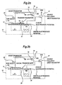
- Fig. 2 is a schematic illustration of the 3 transistor photogate pixel architecture for an Active Pixel Sensor (APS) as envisioned by the present invention.
- the embodiment shown in Fig. 2 envisions the best mode known to inventor.
- Other physical embodiments are realizable that are obvious variations of the embodiment shown in Fig. 2 , as will be discussed further blow.
- the pixel 10 shown in Figs. 2a and 2b is a single pixel within an array of pixels having numerous rows and columns.
Claims (8)
- Aktiver Pixelsensor mit einer Vielzahl von Pixeln, die mindestens ein Pixel (10) umfassen, das aufweist:einen Photogate-Photodetekter (12), der in Wirkverbindung mit einem Ladung-zu-Spannung-Konvertierungsknotenpunkt steht;einen Reset-Trasistor (4) mit einer Source, die an den Ladung-zu-Spannung-Konvertierungsknotenpunkt angeschlossen ist, einem Gate (15), das an einen Reset Control Bus angeschlossen ist, und einem Drain (18), der an einen Knotenpunkt angeschlossen ist, der sowohl mit dem Photogate-Photodetektor (12) als auch mit einem Reihenauswahl-/Photogate Control Bus (26) verbunden ist; undeinen Transistorverstärker (21) mit einer Source, die an einen Ausgangsbus angeschlossen ist, und mit einem Gate, das sowohl an den Ladung-zu-Spannung-Konvertierungsknotenpunkt als auch an die Source des Reset-Transistors (14) angeschlossen ist.
- Aktiver Pixelsensor nach Anspruch 1, worin der Ladung-zu-Spannung-Konvertierungsknotenpunkt eine schwemmende Diffusion (25) aufweist.
- Aktiver Pixelsensor nach Anspruch 1, mit einem Transfer-Gate (23), das den Photo gate-Photodetektor (12) an den Ladung-zu-Spannung-Konvertierungsknotenpunkt anschließt.
- Aktiver Pixelsensor nach Anspruch 1, mit einem virtuellen Transfer-Gate (35), das den Photogate-Photodetektor (12) an den Ladung-zu-Spannung-Konvenierungsknotenpunkt abschließt.
- Verfahren zum Herstellen eines aktiven Pixelsensors, mit den Schritten;Bereitstellen eines Pixels (10) mit einer Photogate-Photodetektor (12), der in Wirkverbindung mit einem Ladung-zu-Spannung-Konvwierungsmittel steht;Herstellen eines Reset-Transistors (14) innerhalb des Pixels (10), der einen Drain (18) aufweist, der an einen Knotenpunkt angeschlossen ist, der sowohl mit dem Photogate-Photodetektor (12) als auch mit einem Reihenauswahl-/Photogate Control Bus (26) verbunden ist, ein Gate (15), das an eines Reset Control Bus angeschlossen ist, und eine Source, die an das Ladung-zu-Spannung-Konvertierungsmittel angeschlossen ist; undHerstellen eines Transistorverstärkers (21) mit einer Source, die an einen Ausgangsbus angeschlossen ist, und mit einem Gate, das sowohl an die Ladung-zu-Spannung-Konvertierungsmittel als auch an die Source des Reset-Transistors (14) angeschlossen ist.
- Verfahren nach Anspruch 5. worin der Schritt des Herstellens außerdem das Herstellen von Mitteln umfasst zum Anlegen einer Kombination aus Signalen an den Reihenauswahl-/Photogate Control Bus (26) und an den Reset Control Bus, um die Ladung-zu-Spannung-Konvertierungsmittel zurückzusetzen.
- Verfahren nach Anspruch 5, worin der Schritt des Herstellens außerdem das Herstellen von Mitteln umfaßt zum Anlegen einer Kombination aus Signalen an den Reihenauswahl-/Photogate Control Bus (26) und an den Reset Control Bus, die derart funktionieren, dass die Reihe ausgewählt wird, die dem Pixel (10) zugeordnet ist
- Verfahren nach Anspruch 5, worin der Schritt des Herstellens außerdem das Herstellen von Mitteln umfasst zum Anlegen einer Kombination aus Signalen an den Reihenauswahl-/Photogate Control Bus (26) und an den Reset Control Bus, um die Reihe zu deselektieren, die dem Pixel (10) zugeordnet ist.
Applications Claiming Priority (2)
| Application Number | Priority Date | Filing Date | Title |
|---|---|---|---|
| US223039 | 1998-12-30 | ||
| US09/223,039 US6624850B1 (en) | 1998-12-30 | 1998-12-30 | Photogate active pixel sensor with high fill factor and correlated double sampling |
Publications (3)
| Publication Number | Publication Date |
|---|---|
| EP1017107A2 EP1017107A2 (de) | 2000-07-05 |
| EP1017107A3 EP1017107A3 (de) | 2003-01-22 |
| EP1017107B1 true EP1017107B1 (de) | 2011-06-22 |
Family
ID=22834757
Family Applications (1)
| Application Number | Title | Priority Date | Filing Date |
|---|---|---|---|
| EP99204062A Expired - Lifetime EP1017107B1 (de) | 1998-12-30 | 1999-12-01 | Photogate Bildelement mit hohem Füllfaktor und doppelter korrelierter Signalabtastung |
Country Status (5)
| Country | Link |
|---|---|
| US (1) | US6624850B1 (de) |
| EP (1) | EP1017107B1 (de) |
| JP (1) | JP4402786B2 (de) |
| KR (1) | KR20000048438A (de) |
| TW (1) | TW453112B (de) |
Families Citing this family (36)
| Publication number | Priority date | Publication date | Assignee | Title |
|---|---|---|---|---|
| US6724426B1 (en) * | 1999-03-08 | 2004-04-20 | Micron Technology, Inc. | Multi junction APS with dual simultaneous integration |
| US7324144B1 (en) * | 1999-10-05 | 2008-01-29 | Canon Kabushiki Kaisha | Solid image pickup device, image pickup system and method of driving solid image pickup device |
| US7129979B1 (en) * | 2000-04-28 | 2006-10-31 | Eastman Kodak Company | Image sensor pixel for global electronic shuttering |
| KR100507879B1 (ko) * | 2000-08-31 | 2005-08-17 | 매그나칩 반도체 유한회사 | Cmos이미지 센서의 단위 화소 |
| US6900839B1 (en) * | 2000-09-29 | 2005-05-31 | Rockwell Science Center, Llc | High gain detector amplifier with enhanced dynamic range for single photon read-out of photodetectors |
| CA2358223A1 (en) * | 2001-01-11 | 2002-07-11 | Symagery Microsystems Inc. | A row decoding scheme for double sampling in 3t pixel arrays |
| US7212240B1 (en) * | 2001-05-25 | 2007-05-01 | Dalsa, Inc. | Imager with a row of photodiodes or pinned photo diodes |
| JP2005513899A (ja) | 2001-12-21 | 2005-05-12 | コーニンクレッカ フィリップス エレクトロニクス エヌ ヴィ | 撮像装置およびこれを備えるカメラ |
| KR100873280B1 (ko) * | 2002-10-31 | 2008-12-11 | 매그나칩 반도체 유한회사 | 향상된 리셋 트랜지스터를 구비한 시모스 이미지센서의단위화소 |
| US7046284B2 (en) * | 2003-09-30 | 2006-05-16 | Innovative Technology Licensing Llc | CMOS imaging system with low fixed pattern noise |
| US20050083421A1 (en) * | 2003-10-16 | 2005-04-21 | Vladimir Berezin | Dynamic range enlargement in CMOS image sensors |
| JP4107269B2 (ja) * | 2004-02-23 | 2008-06-25 | ソニー株式会社 | 固体撮像装置 |
| US7158181B2 (en) * | 2004-05-04 | 2007-01-02 | Andrew G. Cartlidge | System and methods for increasing fill-factor on pixelated sensor arrays |
| US7738026B2 (en) * | 2005-05-02 | 2010-06-15 | Andrew G. Cartlidge | Increasing fill-factor on pixelated sensors |
| DE602004017969D1 (de) * | 2004-06-05 | 2009-01-08 | St Microelectronics Res & Dev | Bildsensor mit geteilten Rücksetz-Signalen und Zeilenauswahl |
| TWI237998B (en) * | 2004-06-09 | 2005-08-11 | Via Tech Inc | Operation of imaging-sensing unit and imaging-sensing device with the same |
| US7340631B2 (en) * | 2004-07-23 | 2008-03-04 | Hewlett-Packard Development Company, L.P. | Drift-tolerant sync pulse circuit in a sync pulse generator |
| US20080128592A1 (en) * | 2004-12-21 | 2008-06-05 | Kazuaki Sawada | Light Receiving Element |
| US7468532B2 (en) * | 2005-07-12 | 2008-12-23 | Aptina Imaging Corporation | Method and apparatus providing capacitor on an electrode of an imager photosensor |
| JP4486015B2 (ja) * | 2005-09-13 | 2010-06-23 | パナソニック株式会社 | 固体撮像装置 |
| KR100790228B1 (ko) * | 2005-12-26 | 2008-01-02 | 매그나칩 반도체 유한회사 | 시모스 이미지 센서 |
| JP4764243B2 (ja) | 2006-04-20 | 2011-08-31 | 株式会社東芝 | 固体撮像装置 |
| JP4873385B2 (ja) * | 2006-07-19 | 2012-02-08 | オリンパス株式会社 | 固体撮像装置 |
| US7915702B2 (en) * | 2007-03-15 | 2011-03-29 | Eastman Kodak Company | Reduced pixel area image sensor |
| US7969494B2 (en) | 2007-05-21 | 2011-06-28 | Aptina Imaging Corporation | Imager and system utilizing pixel with internal reset control and method of operating same |
| KR100885921B1 (ko) * | 2007-06-07 | 2009-02-26 | 삼성전자주식회사 | 후면으로 수광하는 이미지 센서 |
| US20090103827A1 (en) * | 2007-10-19 | 2009-04-23 | John Ladd | Methods, systems, and apparatuses that compensate for noise generated in an imager device |
| US8513709B2 (en) * | 2009-07-27 | 2013-08-20 | Samsung Electronics Co., Ltd. | Photo detecting apparatus and unit pixel thereof |
| KR101588459B1 (ko) * | 2009-08-20 | 2016-01-25 | 주식회사 동부하이텍 | 이미지 센서 및 그 구동 방법 |
| US8441052B2 (en) * | 2009-10-21 | 2013-05-14 | Hiok Nam Tay | Color-optimized image sensor |
| JP5238673B2 (ja) * | 2009-11-09 | 2013-07-17 | 株式会社東芝 | 固体撮像装置 |
| KR101652933B1 (ko) * | 2010-02-17 | 2016-09-02 | 삼성전자주식회사 | 센서, 이의 동작 방법, 및 이를 포함하는 거리 측정 장치 |
| JP2012006257A (ja) * | 2010-06-24 | 2012-01-12 | Canon Inc | 画像処理装置および画像処理方法 |
| JP5511541B2 (ja) * | 2010-06-24 | 2014-06-04 | キヤノン株式会社 | 固体撮像装置及び固体撮像装置の駆動方法 |
| CN102957880B (zh) * | 2012-11-22 | 2015-08-05 | 北京思比科微电子技术股份有限公司 | 一种有源像素、高动态范围图像传感器及操作有源像素的方法 |
| US9526468B2 (en) | 2014-09-09 | 2016-12-27 | General Electric Company | Multiple frame acquisition for exposure control in X-ray medical imagers |
Family Cites Families (16)
| Publication number | Priority date | Publication date | Assignee | Title |
|---|---|---|---|---|
| US5153420A (en) * | 1990-11-28 | 1992-10-06 | Xerox Corporation | Timing independent pixel-scale light sensing apparatus |
| JP3018546B2 (ja) * | 1991-03-18 | 2000-03-13 | ソニー株式会社 | 固体撮像装置 |
| US5841126A (en) | 1994-01-28 | 1998-11-24 | California Institute Of Technology | CMOS active pixel sensor type imaging system on a chip |
| US5471515A (en) | 1994-01-28 | 1995-11-28 | California Institute Of Technology | Active pixel sensor with intra-pixel charge transfer |
| US5631704A (en) | 1994-10-14 | 1997-05-20 | Lucent Technologies, Inc. | Active pixel sensor and imaging system having differential mode |
| US5625210A (en) | 1995-04-13 | 1997-04-29 | Eastman Kodak Company | Active pixel sensor integrated with a pinned photodiode |
| US5587596A (en) | 1995-09-20 | 1996-12-24 | National Semiconductor Corporation | Single MOS transistor active pixel sensor cell with automatic anti-blooming and wide dynamic range |
| US5608243A (en) | 1995-10-19 | 1997-03-04 | National Semiconductor Corporation | Single split-gate MOS transistor active pixel sensor cell with automatic anti-blooming and wide dynamic range |
| US5923794A (en) * | 1996-02-06 | 1999-07-13 | Polaroid Corporation | Current-mediated active-pixel image sensing device with current reset |
| US5721425A (en) | 1996-03-01 | 1998-02-24 | National Semiconductor Corporation | Active pixel sensor cell that reduces the effect of 1/f noise, increases the voltage range of the cell, and reduces the size of the cell |
| US5789774A (en) | 1996-03-01 | 1998-08-04 | Foveonics, Inc. | Active pixel sensor cell that minimizes leakage current |
| US5838650A (en) | 1996-06-26 | 1998-11-17 | Lucent Technologies Inc. | Image quality compensation method and apparatus for holographic data storage system |
| US5786623A (en) | 1996-10-22 | 1998-07-28 | Foveonics, Inc. | Bipolar-based active pixel sensor cell with metal contact and increased capacitive coupling to the base region |
| US5760458A (en) | 1996-10-22 | 1998-06-02 | Foveonics, Inc. | Bipolar-based active pixel sensor cell with poly contact and increased capacitive coupling to the base region |
| US5847422A (en) | 1997-05-19 | 1998-12-08 | Foveonics, Inc. | MOS-based active pixel sensor cell that utilizes the parasitic bipolar action of the cell to output image data |
| US6587146B1 (en) | 1998-11-20 | 2003-07-01 | Eastman Kodak Company | Three transistor active pixel sensor architecture with correlated double sampling |
-
1998
- 1998-12-30 US US09/223,039 patent/US6624850B1/en not_active Expired - Lifetime
-
1999
- 1999-10-30 TW TW088118905A patent/TW453112B/zh not_active IP Right Cessation
- 1999-12-01 EP EP99204062A patent/EP1017107B1/de not_active Expired - Lifetime
- 1999-12-28 KR KR1019990063211A patent/KR20000048438A/ko not_active Application Discontinuation
-
2000
- 2000-01-04 JP JP2000000074A patent/JP4402786B2/ja not_active Expired - Lifetime
Also Published As
| Publication number | Publication date |
|---|---|
| EP1017107A3 (de) | 2003-01-22 |
| TW453112B (en) | 2001-09-01 |
| JP4402786B2 (ja) | 2010-01-20 |
| EP1017107A2 (de) | 2000-07-05 |
| KR20000048438A (ko) | 2000-07-25 |
| US6624850B1 (en) | 2003-09-23 |
| JP2000209504A (ja) | 2000-07-28 |
Similar Documents
| Publication | Publication Date | Title |
|---|---|---|
| EP1017107B1 (de) | Photogate Bildelement mit hohem Füllfaktor und doppelter korrelierter Signalabtastung | |
| EP1017231B1 (de) | Aktiver Bildsensor mit geteilten Rücksetz-Signalen und Zeilenauswahl | |
| EP0898312B1 (de) | Bildsensor mit aktivem Pixel mit geteiltem Ablesungsverstärker | |
| EP1003220B1 (de) | Aktiver Bildsensorarchitektur zur doppelt korrelierten Abtastung mit drei Transistoren | |
| JP3734717B2 (ja) | イメージセンサ | |
| US7542085B2 (en) | Image sensor with a capacitive storage node linked to transfer gate | |
| US10032825B2 (en) | Image sensor with a gated storage node linked to transfer gate | |
| US7375748B2 (en) | Differential readout from pixels in CMOS sensor | |
| US7489352B2 (en) | Wide dynamic range pinned photodiode active pixel sensor (APS) | |
| US5739562A (en) | Combined photogate and photodiode active pixel image sensor | |
| US6552323B2 (en) | Image sensor with a shared output signal line | |
| US6326230B1 (en) | High speed CMOS imager with motion artifact supression and anti-blooming | |
| JP4372789B2 (ja) | 2段階変換利得イメージャ | |
| JP2003333431A (ja) | 固体撮像装置とその駆動方法 |
Legal Events
| Date | Code | Title | Description |
|---|---|---|---|
| PUAI | Public reference made under article 153(3) epc to a published international application that has entered the european phase |
Free format text: ORIGINAL CODE: 0009012 |
|
| AK | Designated contracting states |
Kind code of ref document: A2 Designated state(s): AT BE CH CY DE DK ES FI FR GB GR IE IT LI LU MC NL PT SE |
|
| AX | Request for extension of the european patent |
Free format text: AL;LT;LV;MK;RO;SI |
|
| PUAL | Search report despatched |
Free format text: ORIGINAL CODE: 0009013 |
|
| AK | Designated contracting states |
Kind code of ref document: A3 Designated state(s): AT BE CH CY DE DK ES FI FR GB GR IE IT LI LU MC NL PT SE |
|
| AX | Request for extension of the european patent |
Free format text: AL;LT;LV;MK;RO;SI |
|
| RIC1 | Information provided on ipc code assigned before grant |
Free format text: 7H 01L 27/148 A, 7H 01L 27/146 B |
|
| 17P | Request for examination filed |
Effective date: 20030704 |
|
| AKX | Designation fees paid |
Designated state(s): DE FR GB IT NL |
|
| 17Q | First examination report despatched |
Effective date: 20080725 |
|
| GRAP | Despatch of communication of intention to grant a patent |
Free format text: ORIGINAL CODE: EPIDOSNIGR1 |
|
| GRAS | Grant fee paid |
Free format text: ORIGINAL CODE: EPIDOSNIGR3 |
|
| GRAA | (expected) grant |
Free format text: ORIGINAL CODE: 0009210 |
|
| AK | Designated contracting states |
Kind code of ref document: B1 Designated state(s): DE FR GB IT NL |
|
| REG | Reference to a national code |
Ref country code: GB Ref legal event code: FG4D |
|
| REG | Reference to a national code |
Ref country code: DE Ref legal event code: R096 Ref document number: 69943513 Country of ref document: DE Effective date: 20110804 |
|
| RAP2 | Party data changed (patent owner data changed or rights of a patent transferred) |
Owner name: OMNIVISION TECHNOLOGIES, INC. |
|
| REG | Reference to a national code |
Ref country code: NL Ref legal event code: T3 |
|
| REG | Reference to a national code |
Ref country code: NL Ref legal event code: T3 |
|
| PLBE | No opposition filed within time limit |
Free format text: ORIGINAL CODE: 0009261 |
|
| STAA | Information on the status of an ep patent application or granted ep patent |
Free format text: STATUS: NO OPPOSITION FILED WITHIN TIME LIMIT |
|
| 26N | No opposition filed |
Effective date: 20120323 |
|
| REG | Reference to a national code |
Ref country code: NL Ref legal event code: V1 Effective date: 20120701 |
|
| REG | Reference to a national code |
Ref country code: DE Ref legal event code: R097 Ref document number: 69943513 Country of ref document: DE Effective date: 20120323 |
|
| PG25 | Lapsed in a contracting state [announced via postgrant information from national office to epo] |
Ref country code: IT Free format text: LAPSE BECAUSE OF NON-PAYMENT OF DUE FEES Effective date: 20111201 |
|
| PG25 | Lapsed in a contracting state [announced via postgrant information from national office to epo] |
Ref country code: NL Free format text: LAPSE BECAUSE OF NON-PAYMENT OF DUE FEES Effective date: 20120701 |
|
| REG | Reference to a national code |
Ref country code: FR Ref legal event code: PLFP Year of fee payment: 17 |
|
| REG | Reference to a national code |
Ref country code: FR Ref legal event code: PLFP Year of fee payment: 18 |
|
| REG | Reference to a national code |
Ref country code: FR Ref legal event code: PLFP Year of fee payment: 19 |
|
| PGFP | Annual fee paid to national office [announced via postgrant information from national office to epo] |
Ref country code: DE Payment date: 20181114 Year of fee payment: 20 |
|
| PGFP | Annual fee paid to national office [announced via postgrant information from national office to epo] |
Ref country code: FR Payment date: 20181119 Year of fee payment: 20 Ref country code: GB Payment date: 20181129 Year of fee payment: 20 |
|
| REG | Reference to a national code |
Ref country code: DE Ref legal event code: R071 Ref document number: 69943513 Country of ref document: DE |
|
| REG | Reference to a national code |
Ref country code: GB Ref legal event code: PE20 Expiry date: 20191130 |
|
| PG25 | Lapsed in a contracting state [announced via postgrant information from national office to epo] |
Ref country code: GB Free format text: LAPSE BECAUSE OF EXPIRATION OF PROTECTION Effective date: 20191130 |