EP1013032B1 - Methode et dispositif correspondant permettant d'introduire des jeux de signaux dans un train de signaux et de les extraire - Google Patents
Methode et dispositif correspondant permettant d'introduire des jeux de signaux dans un train de signaux et de les extraire Download PDFInfo
- Publication number
- EP1013032B1 EP1013032B1 EP98939252A EP98939252A EP1013032B1 EP 1013032 B1 EP1013032 B1 EP 1013032B1 EP 98939252 A EP98939252 A EP 98939252A EP 98939252 A EP98939252 A EP 98939252A EP 1013032 B1 EP1013032 B1 EP 1013032B1
- Authority
- EP
- European Patent Office
- Prior art keywords
- signals
- memory
- signal stream
- signal
- communication devices
- Prior art date
- Legal status (The legal status is an assumption and is not a legal conclusion. Google has not performed a legal analysis and makes no representation as to the accuracy of the status listed.)
- Expired - Lifetime
Links
- 238000000034 method Methods 0.000 title claims description 30
- 230000015654 memory Effects 0.000 claims description 136
- 238000004891 communication Methods 0.000 claims description 62
- 230000005540 biological transmission Effects 0.000 claims description 12
- 230000004044 response Effects 0.000 claims 2
- 238000011144 upstream manufacturing Methods 0.000 description 27
- 230000003287 optical effect Effects 0.000 description 14
- 239000000835 fiber Substances 0.000 description 12
- 239000000284 extract Substances 0.000 description 7
- 241000170006 Bius Species 0.000 description 5
- 230000009977 dual effect Effects 0.000 description 5
- 230000011664 signaling Effects 0.000 description 5
- 230000006870 function Effects 0.000 description 3
- 239000000203 mixture Substances 0.000 description 3
- 238000010420 art technique Methods 0.000 description 2
- 230000008878 coupling Effects 0.000 description 2
- 238000010168 coupling process Methods 0.000 description 2
- 238000005859 coupling reaction Methods 0.000 description 2
- 230000006399 behavior Effects 0.000 description 1
- 238000006243 chemical reaction Methods 0.000 description 1
- 238000001514 detection method Methods 0.000 description 1
- 238000010586 diagram Methods 0.000 description 1
- 230000002452 interceptive effect Effects 0.000 description 1
- 239000000463 material Substances 0.000 description 1
- 239000013307 optical fiber Substances 0.000 description 1
- 230000001360 synchronised effect Effects 0.000 description 1
- 230000009466 transformation Effects 0.000 description 1
Images


Classifications
-
- H—ELECTRICITY
- H04—ELECTRIC COMMUNICATION TECHNIQUE
- H04J—MULTIPLEX COMMUNICATION
- H04J3/00—Time-division multiplex systems
- H04J3/16—Time-division multiplex systems in which the time allocation to individual channels within a transmission cycle is variable, e.g. to accommodate varying complexity of signals, to vary number of channels transmitted
- H04J3/1605—Fixed allocated frame structures
- H04J3/1611—Synchronous digital hierarchy [SDH] or SONET
- H04J3/1617—Synchronous digital hierarchy [SDH] or SONET carrying packets or ATM cells
-
- H—ELECTRICITY
- H04—ELECTRIC COMMUNICATION TECHNIQUE
- H04L—TRANSMISSION OF DIGITAL INFORMATION, e.g. TELEGRAPHIC COMMUNICATION
- H04L12/00—Data switching networks
-
- H—ELECTRICITY
- H04—ELECTRIC COMMUNICATION TECHNIQUE
- H04J—MULTIPLEX COMMUNICATION
- H04J3/00—Time-division multiplex systems
- H04J3/02—Details
- H04J3/08—Intermediate station arrangements, e.g. for branching, for tapping-off
-
- H—ELECTRICITY
- H04—ELECTRIC COMMUNICATION TECHNIQUE
- H04L—TRANSMISSION OF DIGITAL INFORMATION, e.g. TELEGRAPHIC COMMUNICATION
- H04L12/00—Data switching networks
- H04L12/54—Store-and-forward switching systems
- H04L12/56—Packet switching systems
- H04L12/5601—Transfer mode dependent, e.g. ATM
-
- H—ELECTRICITY
- H04—ELECTRIC COMMUNICATION TECHNIQUE
- H04Q—SELECTING
- H04Q11/00—Selecting arrangements for multiplex systems
- H04Q11/04—Selecting arrangements for multiplex systems for time-division multiplexing
- H04Q11/0428—Integrated services digital network, i.e. systems for transmission of different types of digitised signals, e.g. speech, data, telecentral, television signals
- H04Q11/0478—Provisions for broadband connections
-
- H—ELECTRICITY
- H04—ELECTRIC COMMUNICATION TECHNIQUE
- H04J—MULTIPLEX COMMUNICATION
- H04J2203/00—Aspects of optical multiplex systems other than those covered by H04J14/05 and H04J14/07
- H04J2203/0001—Provisions for broadband connections in integrated services digital network using frames of the Optical Transport Network [OTN] or using synchronous transfer mode [STM], e.g. SONET, SDH
- H04J2203/0028—Local loop
- H04J2203/003—Medium of transmission, e.g. fibre, cable, radio
- H04J2203/0032—Fibre
-
- H—ELECTRICITY
- H04—ELECTRIC COMMUNICATION TECHNIQUE
- H04J—MULTIPLEX COMMUNICATION
- H04J2203/00—Aspects of optical multiplex systems other than those covered by H04J14/05 and H04J14/07
- H04J2203/0001—Provisions for broadband connections in integrated services digital network using frames of the Optical Transport Network [OTN] or using synchronous transfer mode [STM], e.g. SONET, SDH
- H04J2203/0046—User Network Interface
- H04J2203/0048—Network termination, e.g. NT1, NT2, PBX
-
- H—ELECTRICITY
- H04—ELECTRIC COMMUNICATION TECHNIQUE
- H04J—MULTIPLEX COMMUNICATION
- H04J2203/00—Aspects of optical multiplex systems other than those covered by H04J14/05 and H04J14/07
- H04J2203/0001—Provisions for broadband connections in integrated services digital network using frames of the Optical Transport Network [OTN] or using synchronous transfer mode [STM], e.g. SONET, SDH
- H04J2203/0089—Multiplexing, e.g. coding, scrambling, SONET
-
- H—ELECTRICITY
- H04—ELECTRIC COMMUNICATION TECHNIQUE
- H04L—TRANSMISSION OF DIGITAL INFORMATION, e.g. TELEGRAPHIC COMMUNICATION
- H04L12/00—Data switching networks
- H04L12/54—Store-and-forward switching systems
- H04L12/56—Packet switching systems
- H04L12/5601—Transfer mode dependent, e.g. ATM
- H04L2012/5638—Services, e.g. multimedia, GOS, QOS
- H04L2012/5646—Cell characteristics, e.g. loss, delay, jitter, sequence integrity
- H04L2012/5652—Cell construction, e.g. including header, packetisation, depacketisation, assembly, reassembly
-
- Y—GENERAL TAGGING OF NEW TECHNOLOGICAL DEVELOPMENTS; GENERAL TAGGING OF CROSS-SECTIONAL TECHNOLOGIES SPANNING OVER SEVERAL SECTIONS OF THE IPC; TECHNICAL SUBJECTS COVERED BY FORMER USPC CROSS-REFERENCE ART COLLECTIONS [XRACs] AND DIGESTS
- Y10—TECHNICAL SUBJECTS COVERED BY FORMER USPC
- Y10S—TECHNICAL SUBJECTS COVERED BY FORMER USPC CROSS-REFERENCE ART COLLECTIONS [XRACs] AND DIGESTS
- Y10S370/00—Multiplex communications
- Y10S370/916—Multiplexer/demultiplexer
Definitions
- the signal stream can contain a mixture of cells having asynchronous application signals (i.e., signals for asynchronous communication applications) and cells having isochronous application signals (i.e., signals for isochronous applications).
- asynchronous application signals i.e., signals for asynchronous communication applications
- isochronous application signals i.e., signals for isochronous applications
- Integrated telecommunication systems that carry different types of signals for different types of applications, have to properly multiplex and demultiplex the different signals in the signal stream.
- some integrated broadband/narrowband systems have to separate the isochronous application signals (e.g., such as telephony signals) from the asynchronous application signals (e.g., video and data signals).
- a simple prior art method for extracting isochronous telephony signals reads all of the bytes in a received frame into a memory and subsequently determines the isochronous bytes.
- Figures 1 and 2 set forth one implementation of this prior art technique.
- the prior art includes a memory 105 which sequentially stores every byte of a received frame in contiguous byte-wide memory locations.
- This prior art implementation also includes a table of pointers 110 with a pointer for each memory location.
- Each pointer for a memory location that stores telephony bytes points to a specific twisted pair 210 of a specific telephone-interface-unit (TIU) card 205, as set forth in Figure 2 .
- TIU telephone-interface-unit
- WO 97/27550 describes a communication system with multicarrier telephony transport, where the communication system includes a head end that provides for downstream transmission of telephony and control data in a first frequency bandwidth over a hybrid fiber/coax distribution network and reception of upstream telephony and control data in a second frequency bandwidth over the hybrid/coax distribution network.
- the invention provides method and apparatus for identifying signals for a set of communication devices in a signal stream having signals for a number of different sets of communication devices.
- an apparatus and method according to the accompany claims Some embodiments of the invention are methods and devices for extracting signals for a first set of communication devices from a signal stream having signals for a number of different sets of communication devices.
- Other embodiments of the invention are methods and devices for inserting into a signal stream signals from a first set of communication devices.
- Yet other embodiments of the invention are time division multiplexing and demultiplexing methods and apparatuses that use a content addressable memory to identify sets of signals for a particular set of communication devices.
- some embodiment of the invention are used in fiber optic telecommunication networks. These embodiments include an optical network unit that receives an integrated signal stream having signals for different types of applications.
- the optical network unit includes a content addressable memory that stores locations in the received signal stream of signals for a first type of communication application.
- a communication device is a device that transmits and/or receives signals through the communication system.
- Examples of such communication devices include computers (such as network computers, personal computers, workstations, servers, etc.), television set-top boxes, premises interface device, and telephones.
- One or more communication devices form each set of communication devices.
- a set of communication devices can include similar communication devices (e.g., a set of telephony communication devices can use similar telephony equipment).
- a set of communication devices can be defined by a number of communication devices that utilize a similar communication medium (e.g., utilize twisted pairs or co-axial cables) to connect to the communication system.
- a set of communication devices can be defined by a number of communication devices that utilize similar communication-medium terminating devices (e.g., utilize similar line cards, adapter cards, modems, etc.).
- the FTTC network 300 connects one or more communication devices at one or more network subscriber site 305 to one or more communication networks, such as a public switched telecommunications network (PSTN) 310, an asynchronous transfer mode (ATM) network 315, or other communication networks.
- PSTN public switched telecommunications network
- ATM asynchronous transfer mode network 315
- Each network subscriber site 305 can be residential or commercial subscriber sites.
- the FTTC network 300 transmits signal streams between the subscriber sites and the PSTN 310, the ATM network 315, or other networks (e.g., individual, private, or non-switched public networks).
- the signal streams contain signals transmitted to, or received from, a number of sets of communication devices.
- the FTTC network transmits signals to and from telephony communication devices (i.e., telephony application signals) and signals to and from non-telephony communication devices (i.e., non-telephony application signals).
- signals for different types of communication devices can be transmitted through the communications network.
- the FTTC network 300 includes a host digital terminal (HDT) 320, element management system (EMS) 325, a number of fiber optic cables 330, and a number of optical network units (ONUs) 335.
- the HDT couples to the PSTN, the ATM network, and/or other networks.
- the PSTN-HDT interface 340 follows the specification adopted by one of the standards bodies, such as the Bellcore specification TR-TSY-000008, TR-NWT-000057 or TR-NWT-000303.
- the physical interface to the PSTN can be twisted pairs carrying DS 1 signals, or fiber optic cables carrying OC-3 optical signals.
- the ATM network-HDT interface 345 can be realized using an optical interface (such as OC-3, OC-12c, etc.).
- the HDT 320 has two optical broadcast ports, which can only receive signals carrying ATM cells, and one optical interactive port which can receive and transmit signals.
- the HDT receives downstream signals from the PSTN, the ATM network, or other networks, and routes these signals downstream to the network subscriber sites. It also receives upstream signals from the network subscriber sites, and routes these signals upstream to the PSTN, the ATM network, or other networks:
- the HDT serves a multiplexor which (1) controls access of the received downstream signals (i.e., the signals it receives from the PSTN, ATM, or other networks) to the transmission media, and (2) transmits the received signals to the appropriate ONUs 335 via the appropriate fiber optic cables 330.
- the HDT serves as a demultiplexor which (1) parses the received upstream signals (i.e., the signals received from the ONUs) into signal streams for the PSTN, ATM, or other networks, and (2) supplies these signal streams to the appropriate network.
- the HDT also re-formats the downstream and upstream signals, before forwarding them to their destinations. As further described below, the HDT performs the following formatting operations: combining isochronous and asynchronous signals into frames, parsing integrated frames into individual signal streams, adjusting signal rates, and converting of electrical signals to and from optical signals.
- formatting operations include combining isochronous and asynchronous signals into frames, parsing integrated frames into individual signal streams, adjusting signal rates, and converting of electrical signals to and from optical signals.
- the HDT does not perform all of these formatting operations, or performs additional operations.
- the HDT combines (i.e., maps) the received downstream signals into frames containing a mixture of cells having asynchronous application signals (such as data and video signals) and cells having isochronous application signals (such as telephony signals).
- the HDT transmits these frames to the ONUs at a prespecified rate (e.g., once every 125 ⁇ s).
- the HDT also parses the received upstream frames into individual bytes supplied to the PSTN, ATM, or other networks.
- FIG. 4 presents one example of frames transmitted across the fiber optic cables 330.
- Each frame shown in this figure is a SDH-like frame which includes overhead and payload envelopes.
- the payload envelope includes 41 cells of asynchronous and isochronous information. Each cell has 57 bytes.
- Figure 5 presents one example of an isochronous, telephony cell. As shown in this figure, each cell includes three reserved bytes (R), and six groups of DS0 bytes. Figure 5 presents each group as eight DS0 data bytes following one signaling byte (S). The signaling byte contains the status and control signals (e.g., on/off hook, ring, etc.) for the eight DS0 bytes. Alternatively, each group can include nine clear DSOs bytes containing a mix of information and control signals.
- R reserved bytes
- S signaling byte
- S signaling byte
- the signaling byte contains the status and control signals (e.g., on/off hook, ring, etc.) for the eight DS0 bytes.
- each group can include nine clear DSOs bytes containing a mix of information and control signals.
- the HDT also adjusts the signal rate of the data it receives. For instance, for some embodiments of the invention, the HDT 320 converts the signals it receives from the PSTN 310 at a DS1-rate to signals at a DS0-rate; it then transmits these signals to the ONUs in the SDH-like frames. On the upstream side, the HDT performs the inverse signal rate transformation operation. The HDT also converts the electrical representation of the digital signals into an optical representation, and visa versa.
- the HDT couples to the EMS 325.
- the EMS is used to provision services and equipment on the FTTC network (e.g., allocate twisted pairs off the TIUs), in the central office where the HDT 320 is located, in the field, or in the residences.
- the EMS is software based and can run on a personal computer in which case it will support one HDT and the associated access network equipment connected to it. Alternatively, it can run on a workstation in which case it will support multiple HDTs and access networks.
- the fiber optic cables 330 communicatively couple the HDT to a number of ONUs 335 located in a number of serviced areas.
- Some embodiments of the invention use bi-directional, single-mode fiber lines and a dual wavelength transmission scheme to communicate between the ONUs and the HDT.
- some embodiments of the invention use sixty four optical fiber cables to connect the HDT to sixty four ONUs.
- each ONU includes a common control unit (CCU) 350, four telephone interface units (TIU) 355, and eight broadband interface units (BIU) 360.
- the CCU controls the operation of the ONU.
- the CCU performs similar formatting operations as those performed by the HDT.
- the CCU (1) parses the received downstream signals (i.e., the frames it receives from the HDT) into telephony application signal streams and non-telephony application signal streams, and (2) supplies the telephony application signal streams to the appropriate TIU 355.
- the CCU also combines the signal streams that it receives from the TIUs 355 and BIUs 360 into SDH-like frames (such as the frames discussed above with respect to Figure 4 ), which it then transmits to the HDT via fiber optic cable 330.
- Different embodiments of the invention can be employed in the CCU, in order to allow the CCU to perform the above-described parsing (i.e., demultiplexing) and combining (i.e., multiplexing) operations. Two such embodiments will be described below by reference to Figures 7 and 11 .
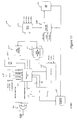
- Figure 6 presents one example of the CCU 350.
- the CCU includes a bi-directional (BIDI) optical converter 605, a framer 610, a TIU interface (TIUI) 615, a BIU interface (BIUI) 620, and a microprocessor 625.
- the optical converter 605 converts optical signals, that it receives via a fiber optic cable 330, into a serial, electrical signal stream.
- the framer 610 then receives this bit-wide electrical signal stream and converts it into a byte-wide signal stream.
- the optical converter receives bit-wide, electrical signals from the framer, and converts these electrical signals into optical signals for transmission via the fiber optic cable 330.
- the framer also scans the incoming signal stream in order to determine the frame boundary information used to determine the location of payload and overhead bytes. Once the framer determines the frame boundary, it generates a frame synch signal which indicates the start of each frame. As described below, this frame synch signal is used by a number of the circuits of the CCU.
- the framer communicatively couples to the TIUI 615, in order to transmit and receive signals from the TIUI.
- Some embodiments of the invention are implemented in the TIUI, in order to allow the TIUI to parse the telephony application signals from the downstream signal stream, and to combine the telephony application signals into the upstream signal stream. Two such embodiments will be described below by reference to Figures 7 and 11 .
- the framer also transmits signals to and receives signals from the BIUI.
- the BIUI performs administrative functions (e.g., parity check and overhead addition functions).
- the BIUI forwards the signals it receives from the framer to the BIUs 360.
- Each individual BIU then extracts the portion of the received signals that are addressed to it; the BIU forwards the extracted signals to a network subscriber site 305.
- the BIUI 620 acts as an arbitrator for the BIUs. In this capacity, the BIUI allocates different portions of each frame's payload to different BIU's.
- the microprocessor 625 of the CCU 350 is used to program various components of the CCU. For instance, as further described below, the microprocessor is used to program various components of the TIUI. Through this programming, the TIUI can store the location of telephony bytes in the received or transmitted signal stream.
- each ONU 335 includes four TIUs 355 coupled to the TIUI 615 through a backplane interconnect.
- Each TIU 355 connects to six twisted pairs 365, which thereby allow each ONU to service up to twenty four network subscriber sites.
- the FTTC network 300 utilizes ONUs that have different number of TIUs and/or different number of twisted pairs for each TIU.
- a TIU When a TIU receives a signal stream from the CCU, it converts the signal stream into a signal stream for a narrowband service (such as plain old telephony signals (POTS), coin, ISDN, etc.). For instance, the TIU can generate analog POTS which it transmits to network subscriber site 305 via a twisted pair 365.
- a network interface device (NID) 370 serves as an interface and demarcation point between the twisted pair 365 and subscriber-site twisted pair 375 coupled to telephone 380.
- the NID provides high-voltage protection.
- each TIU 355 receives analog signals from the network subscriber site. It then converts these analog signals into digital signals which it supplies to the CCU.
- Each ONU 335 also includes eight BIUs 360 coupled to the CCU 350 through the backplane interconnect.
- Each BIU 360 connects to two co-axial cables. Alternative number of BIUs and/or co-axial cables could also be used in the ONU.
- each BIU communicatively couples to the BIUI 620 of the CCU 350. Through this coupling, the BIU receives signals from the CCU.
- the BIU includes a filter which decodes a portion of the overhead bytes of each received cell to determine if the received cell is addressed to its BIU. If so, the filter also determines the addressed co-axial cable of the BIU. The filter then reformats the received cell and stores it in a FIFO queue. As the contents of the FIFO are read out, the BIU modulates the read-out signals onto an RF carrier and transmits the data via the addressed co-axial cable to a splitter 385 at the network subscriber site 305.
- Subscriber-site coaxial cables 390 couple the splitter to a number of communication devices at the network subscriber site.
- These communication devices include a television (TV) 392 with a television set-top 394, computer with a network interface card (NIC) 396, and a premises interface device (PID) 398 connected to a telephone.
- TV television
- NIC network interface card
- PID premises interface device
- each communication device requires an interface sub-system which provides for the conversion of the signal from the format on the subscriber-site coaxial cable to the service interface required by the device.
- the PID 398 extracts the voice signals carried on the subscriber-site coaxial cable 390 and generates a telephone signal compatible with the telephone.
- the television set-top 394 converts digital video signals to analog signals compatible with the TV 392.
- the NIC card generates a computer compatible signal.
- the BIU Through the subscriber-site coaxial cables 390, the splitter 385, and the coaxial cable 367, the BIU also receives broadband signals for upstream transmission through the FTTC network 300.
- the BIU demodulates the signals that it receives and combines the resulting components of the broadband signals into a unified broadband signal stream, which it relays to the BIUI 620.
- the invention can be implemented in other FTTC networks.
- some embodiments of the invention can be implemented in the networks disclosed in United States Application No. , entitled “Unified Access Platform,” filed on August 4, 1997, concurrently with the present application, having Thomas R. Eames as the inventor, and having the express mail label number EH385539499US.
- the invention can be implemented in alternative networks.
- One embodiment of the invention that is implemented in the FTTC network 300 extracts signals for a set of telephony communication devices from an integrated telephony/non-telephony signal stream transmitted through the FTTC network.
- This embodiment stores position identifying indicia (e.g., pointers) that identify the locations of telephony application signals in a received signal stream, which as mentioned above, is organized in a SDH-like frame.
- the process extracts the telephony signal corresponding to the generated indicia from the received signal stream. This process then generates appropriate routing signals based on the matched stored location, in order to route the extracted set of signals to its set of communication devices.
- FIG. 7 sets forth one such embodiment.
- This apparatus is implemented in the CCU's TIUI 615, and serves as the interface to the TIUs of the ONU 335.
- This interface constantly receives the SDH-like frames in byte-wide increments at the SDH-like 19.44 MHz.
- the interface includes a byte counter 705, a content addressable memory 710, a memory interface unit 715, swing data random access memories 720, a control random access memory (RAM) 725, a downstream TIU interface 730, a table of pointers 735, a pointer RAM control 740, a bit counter (not shown), a microprocessor interface unit 745, and a downstream synchronizing unit (not shown).
- the counter 705 and content addressable memory (CAM) 710 in conjunction act to identify the telephony application signals in the downstream SDH-like frames forwarded to the memory interface unit 715. Specifically, the counter receives frame synchronizing signal (generated by the framer 610) to maintain its alignment to each frame. The counter also receives a synchronizing signal from the downstream synchronizer (not shown). This synchronizing signal maintains the counters in the SDH-domain and the counters in the telephony-domain in synch, so that the interface units 715 and 730 in these domains do not simultaneously access the memories 720 and 725.
- frame synchronizing signal generated by the framer 610
- the counter also receives a synchronizing signal from the downstream synchronizer (not shown). This synchronizing signal maintains the counters in the SDH-domain and the counters in the telephony-domain in synch, so that the interface units 715 and 730 in these domains do not simultaneously access the memories 720 and 725.
- the counter also receives the 19.44 MHz SDH-byte clock to generate three count values that are synchronous with the signals received in byte-wide sets at this frequency.
- the counter is a byte counter which generates sets of count values.
- Each set of count values serves as a pointer that specifies the location of a byte within a frame received by the memory interface unit 715.
- Each pointer is input to the CAM to determine if the received byte corresponding to the pointer is a telephony application byte.
- some embodiments of the invention are designed to multiplex and demultiplex SDH-like frames with a payload of 41 cells of telephony application signals (e.g., TDM signals) and non-telephony applications signals (e.g., ATM signals).
- telephony application signals e.g., TDM signals
- non-telephony applications signals e.g., ATM signals.
- Each telephony cell is composed of 6 groups of 9 bytes. The 9 bytes are arranged as one signaling byte followed by 8 DS0 bytes.
- the counter Given this cell structure, the counter generates (1) a cell count value, RxCellCnt, that specifies the cell count of the currently received byte, (2) a group count value, RxGrpCnt, that specifies the group count of the currently received byte, and (3) a DS0 byte count, RxDS0Cnt, that specifies the byte count of the currently received byte.
- the three count values serve as pointers that uniquely identify every byte within each of the 41 potential TDM cells.
- the DS0 number 8 within each group is used as the super-frame, multiplexed signaling byte. Also, within each cell there are three reserved bytes corresponding to group 7 with a DS0 count of 0, 1 or 2.
- the CAM 710 receives the generated count values (RacCellCnt, RxGrpCnt, and RxDS0Cnt) and receives a signal (RxCellType) indicating the type of the received cell.
- a CAM is a memory device with the ability to compare any set of signals (e.g., a data word) presented to it with all of the CAM contents at once, and report the location in the CAM whose contents match the presented set of signals.
- CAMs have been used in bridges and routers to compare extracted MAC addresses with stored MAC addresses, in order to determine if received packets are addressed to LANs connected to the bridges or routers.
- Figure 8 presents one example of the CAM 710 that can be used in some embodiments of the invention.
- the CAM includes control circuitry 805, a first memory 810, a second memory 815, downstream comparators 820, and decoder 825.
- this figure presents two memories, one of ordinary skill in the art would appreciate that this presentation is simply a pictorial representation of the CAM in order to facilitate its description, and that these two memories could be part of a single memory array.
- the first and second memories couple to the microprocessor 625 to receive respectively data signals (i.e., position identifying indicia) and control signals (e.g., block size indicia) for storing.
- data signals i.e., position identifying indicia
- control signals e.g., block size indicia
- the first memory 810 receives and stores up to thirty two position identifying indicia that identify the position of thirty two telephony-application bytes in each SDH-like frame.
- the first memory stores thirty position identifying indicia, where each position identifying indicia is a pointer that specifies the location of a telephony-application byte within each frame received by memory interface unit.
- each stored pointer can have thirteen bits. Of these bits, six bits identify the cell value, three bits identify the group value, and four bits identify the byte value.
- the microprocessor stores control bits that determine the size of the blocks of signals extracted from the signal stream.
- the second memory stores thirty two sets of control bits, so that there is one set of control bits for each pointer in the first memory. Each set of control bits includes two bits.
- the CAM also includes thirty-two comparators 820. Each comparator compares a particular thirteen-bit pointer stored in the first memory with the thirteen-bit output of the byte counter 705. For instance, the comparator for the nth row in the first memory array receives the bits stored in row n (Rn) from columns 0 to 12 (C0 and C12), and compares these bits to the generated thirteen count bits RxCellCnt, RxGrpCnt, and RxDS0Cnt.
- Each comparator includes thirteen X-NOR gates, with each X-NOR gate receiving one bit of the stored pointer and one bit of the generated count value.
- Each comparator also has an AND gate (not shown) which receives the outputs of the thirteen X-NOR gates of the comparator. The output of each AND gate then represents the output of the comparator.
- the thirty two comparators 820 have thirty two output lines. When a received byte's location matches a stored pointer, the pointer's comparator indicates a hit (i.e., a match) by pulling its output line high.
- a hit i.e., a match
- the memory interface unit 715 receives the thirty two bit output of the comparators 820.
- This interface unit includes a priority encoder which receives this thirty two bit output to generate a five bit output to represent the address of the row storing the matched pointer in the first memory.
- the row address for the matched pointer is the same as the row address for its corresponding pair of control signals in the second memory.
- the five bit address is supplied to the decoder 825 of the second memory.
- This decoder then latches and outputs the two control bits stored at the row identified by the received address signal.
- the memory interface unit then receives these two bits, which, as described later, direct the interface unit to extract up to three bytes that follow the received byte.
- the CAM also receives the CellType signal (such as RxCellType or TxCellType).
- This signal indicates whether the cell that is currently being received in the received frame is a telephony cell or a non-telephony cell.
- the CCU includes a memory (not shown) with forty one registers for the forty one cells in the frame payload. Each register stores a CellType flag that indicates whether its corresponding cell is a telephony cell. By using the cell count address generated by the counter 705, the CCU sequentially reads the forty one registers to generate the CellType signal. When the cell is not a telephony cell, the value of the CellType signal powers down the comparators 820.
- the memory interface unit 715 of Figure 7 receives the downstream signal stream. It also receives the generated count values RxGrpCnt and RxDS0Cnt, and the RxCellType, in order to synchronously operate with the CAM. It couples to the CAM 710 to receive its thirty-two bit output. Based on this output, it generates the five bit address of the matched pointer in the CAM. The interface unit then uses this address to retrieve the two control bits corresponding to the matched pointer from the CAM.
- the interface unit Based on the two control bits, as well as the thirty two output bits of the CAM, the interface unit extracts one to four telephony bytes from the received signal stream, and generates address and control signals to store the extracted telephony bytes in data and control RAMs 725 and 730.
- Figure 9 presents one example of the memory interface unit 715.
- This embodiment includes a priority encoder 905, an OR gate 910, and a downstream (DS) state machine 915.
- Priority encoder 905 receives the thirty two bit output of the CAM. As the CAM does not store identical pointers, only one of the thirty two output lines should be active when a telephony signal is received. If the CAM reports multiple hits on its thirty two output lines (i.e., if more than one line is active), it is determined that the CAM was improperly programmed, and an error condition is reported through an interrupt structure or a status flag.
- the priority encoder When one of the thirty two output lines 755 are active, the priority encoder generates a five bit address based on the values of the active line. This address is sent back to the CAM in order to retrieve two control bits which are stored in the second memory at the generated row address. These two bit are then supplied to the DS state machine.
- the state machine also receives an enable signal 920, as well as the five-bit output of the encoder.
- the enable signal is the output of the OR gate 910, which receives as its input the thirty two output lines of the CAM. When one of these lines is active, the OR gate output is also active. This active signal causes the DS state machine to extract from the downstream signal stream the byte that it is receiving at that time. By decoding the two control bits, the DS state machine then determines whether it needs to extract up to three other bytes that follow the initial, extracted byte.
- the state machine 915 Based on the value of the generated five bit address and the two control bits, the state machine 915 generates address and control signals to store the extracted bytes in the data and control RAMs 720 and 725.
- the relationship between the pointers stored in the CAM and the storage locations in RAMs 720 and 725 (for storing extracted bytes whose locations in the signal stream matched the stored pointers) is hard coded. This hard coded relationship allows the downstream state machine to simply use the five bit row address 925 of the matched pointers to generate the address signals for the locations in the RAMs 720 and 725 for storing the extracted bytes.
- the memory interface unit is designed by using a hardware design language.
- a hardware design language For such embodiments, one possible design of the memory interface unit is set forth in Appendix A. This design uses the Verilog hardware design language. Numerous manufacturers of logic synthesizers (such as Synopsys, Viewlogic, Synplicity, ACEO, Cascade Design Automation, Exemplar, and Altera) can transform the logic in this code to gates, and thereby obtain the gate level implementation for the memory interface unit.
- logic synthesizers such as Synopsys, Viewlogic, Synplicity, ACEO, Cascade Design Automation, Exemplar, and Altera
- the memory interface unit extracts either telephony data signals or telephony control signals from the frame.
- the two signal types are treated differently in the way they are stored.
- the control signals are written to control RAM 725, whereas the data signals are written to data RAM 720.
- the control RAM is a 128x8, dual port RAM, while the data RAM is formed by two 32x32, dual port RAMs that act as a "swing" buffer ("ping-pong" buffer).
- RAMs 720 and 725 are where the telephony data and control signals cross from the 19 MHz, SDH-like time domain into the 4 MHz, telephony domain (e.g., POTS domain). Two RAMs are used to form the "swing" buffer for the telephony data signals.
- the "swing" buffer has two memory areas so the 19 MHz domain can write the data for one frame, while the 4 MHz domain can read the data for the previous frame.
- the memory interface unit 715 determines which of the "swing" RAMs to store the telephony data signals in the current frame, based on a frame count generated by a frame counter (not shown).
- the control signals do not require more than one RAM to cross the 19 MHz - 4 MHz boundary. This is because the frequency of the control signals is slow enough that both the 19 MHz and the 4 MHz domains can access the RAM before the next signaling byte will appear in the SDH frame. Also, a slight degree of imprecision can be tolerated with respect to the control signals, as such imprecision will hardly be noticed by the users.
- the 4 MHz side is given priority over the 19 MHz side in the accessing of this control signal RAM.
- the pointer RAM control 740, the table of pointers 735, and the DS TIU interface 730 direct the telephony signals in RAMs 720 and 725 to the appropriate TIUs.
- the pointer RAM control 740, the table of pointers 735, and the DS TIU interface 730 act as a cross connect structure that determines which data and control is forwarded to which TIU.
- the DS TIU interface 730 couples to four TIUs A, B, C, and D.
- This interface also couples to the pointer control 740 to receive addresses of locations in the data and control RAMs that it needs to read.
- the pointer control retrieves these addresses from the pointer table 735.
- the pointer table couples to the microprocessor 625 through the pointer control 740 and the microprocessor interface unit 745, in order to receive and store address signals from the microprocessor during a program mode.
- the pointer control 740 serves as an arbitor which controls access to the table 735.
- the pointer control receives the 4.096 MHz clock signal, the frame synch signal, and the DS synch signal.
- a bit counter (not shown) of this pointer control receives the 4 MHz clock signal to generate a nine-bit count at this frequency.
- the control unit receives the frame synch signal (generated by the framer 610) to maintain its alignment to each frame.
- the control unit 740 receives the DS synch signal from the downstream synchronizer (not shown), in order to synchronize its counter with the SDH-domain counters so that the interface units 715 and 730 do not simultaneously access the memories 720 and 725.
- the top six bits of the nine-bit count produced by the pointer control's counter serves as a byte counter that counts sixty four bytes for each received frame. These sixty four count values define sixty four time slots during which the pointer control 740 (1) causes the pointer table 735 to generate 256 addresses in the RAMs 720 and 725, and (2) supplies these 256 addresses to the DS TIU interface 730.
- the pointer RAM control directs the table 735 to output in a particular sequence the contents of four of its nine-bit wide storage locations.
- Each nine-bit wide storage location of the table 735 includes seven bits for defining a row address, one bit for selecting the control RAM, and one bit for selecting the data RAM.
- the TIU interface 730 reads the RAMs at each of the four addresses output by the table. The TIU interface then forwards the four sets of retrieved signals to the four TIUs A, B, C, and D.
- Figure 10 illustrates this read out operation pictorially for one embodiment of the invention which stores 120 telephony data bytes in each data RAM 720, and stores 120 telephony control bytes in the control RAM 725.
- the DS TIU interface reads out overhead bytes (e.g., parity bytes).
- Each TIU 355 receives one set of telephony data bytes and one set of telephony control bytes.
- the pointer RAM control 740 alternatively reads out telephony data bytes and telephony control bytes for each TIU.
- Data and control signal fetching are done for each of the TIU in a particular order.
- the DS TIU interface 730 retrieves four telephony bytes, The first three bytes for three TIUs are stored in intermediate registers. When the fourth byte is fetched, all four bytes are written to shift registers. These bytes are then shifted out to the TIUs one bit at a time based on the value of the pointer control's bit counter. While the bytes in the shift registers are being shifted out, the next four telephony bytes are fetched.
- the DS TIU interface 730 and the pointer control 740 are designed and manufactured by using a hardware design language.
- a hardware design language For such embodiments, one possible design for the DS TIU interface unit is set forth in Appendix B, while one possible design for the pointer control 740 is set forth in Appendix C.
- These designs use the Verilog hardware design language. Numerous manufacturers of logic synthesizers (such as Synopsys, Viewlogic, Synplicity, ACEO, Cascade Design Automation, Exemplar, and Altera) can transform the logic in this code to gates, and thereby obtain the gate level implementation for the DS TIU interface.
- Another embodiment of the invention that is implemented in the FTTC network 300 multiplexes telephony application signals and non-telephony application signals to form an integrated telephony/non-telephony signal stream for transmission to the HDT 320 through the FTTC network.
- This embodiment stores position identifying indicia (e.g., pointers) that identify the appropriate location of the telephony signals in a signal stream, which as mentioned above is organized in a SDH-like frame. It then generates position identifying indicia as it receives signals for transmission, and compares the indicia to the stored indicia. When generated indicia matches stored indicia, it inserts the telephony signal corresponding to the generated indicia in the signal stream.
- position identifying indicia e.g., pointers
- Figure 11 sets forth one such embodiment of the invention.
- This embodiment multiplexes telephony signals and non-telephony signals to form an integrated telephony/non-telephony signal stream for transmission to the HDT 320 through the FTTC network.
- the interface apparatus 1100 constantly receives four telephony data streams (e.g., four DS0 streams) from four TIUs A, B, C, and D. It multiplexes these streams with another signal stream to form a byte-wide stream supplied to the framer.
- four telephony data streams e.g., four DS0 streams
- the apparatus 1100 of Figure 11 can be implemented in the CCU's TIUI, which serves as the interface between the TIUs and the fiber optic cables.
- this apparatus has a byte counter 1105, a CAM 1100, a memory interface unit 1115, two dual port data RAMs 1120, a dual port control RAM 1125 , an upstream (US) TIU interface 1130, a table 1135, a pointer control 1140, and a microprocessor interface unit 1145.
- it also includes a delay FIFO 1150, an early counter 1155, and a set of eight OR gates 1160.
- the operation of the apparatus 1100 is similar to the operation of the apparatus 700, except that it is in the reverse order and it has a built in delay.
- the pointer control 1140, the table 1135, and the US TIU interface 1130 act as a cross connect structure.
- the pointer control 1140, the table 1135, and the US TIU interface 1130 forward the signals coming from the TIUs to the RAMs 1120 and 1125.
- the US TIU interface 1130 couples to TIUs A, B, C, and D to receive telephony data and control bytes.
- This interface also couples to the table 1135 via the control unit 1140 to receive addresses of locations in the data and control RAMs 1120 and 1125, in which it can store the received telephony bytes.
- the table 1135 5 couples to the microprocessor 625 through the control unit 1140 and the microprocessor interface unit 1145, in order to receive and store address signals from the microprocessor during a program mode.
- the table 1135 is controlled by the pointer control 1140, which includes a bit counter (not shown).
- This control unit receives the 4.096 MHz clock signal, the frame synch signal, and the US synch signal.
- the control unit's bit counter receives the 4.096 MHz clock signal to generate a nine-bit count at this frequency.
- the control unit receives the frame synch signal (generated by the framer 610) to maintain its alignment to each frame.
- the control unit 1140 receives the US synch signal from the downstream synchronizer (not shown), in order to synchronize its counter with the SDH-domain counters so that the interface units 1115 and 1130 do not simultaneously access the memories 1120 and 1125.
- the top six bits of the nine-bit count produced by the pointer control's counter serves as a counter that counts sixty four time slots for each transmitted frame.
- the pointer control 1140 (1) causes the pointer table 1135 to output 256 addresses in the RAMs 1120 and 1125, and (2) supplies these addresses to the US TIU interface 1130.
- the US TIU interface then uses these 256 addresses to store 256 bytes from the TIUs 355 in the RAM 1120 and 1125.
- the US TIU 1130 receives and stores up to four telephony bytes from the four TIUs A, B, C, and D. Also, during each time slot, the pointer RAM control 1140 directs the table 1135 to output four of its nine-bit wide storage locations. Each nine-bit wide storage location in the table 1135 includes seven bits for defining a row address, one bit for selecting the control RAM, and one bit for selecting the data RAM. The US TIU interface then uses the nine-bit outputs of the table to store its four telephony bytes in the RAMs 1120 and 1125.
- the pointer RAM control 740 is designed and manufactured by using a hardware design language; one example of such a design is set forth in Appendix C.
- the US TIU interface 1130 is designed and manufactured by using a hardware design language.
- one possible design of the US TIU interface is set forth in Appendix D. This design uses the Verilog hardware design language. Numerous manufacturers of logic synthesizers (such as Synopsys, Viewlogic, Synplicity, ACEO, Cascade Design Automation, Exemplar, and Altera) can transform the logic in this code to gates, and thereby obtain the gate level implementation for the US TIU interface.
- the memory interface unit 1115 also accesses the data and control RAMs 1120 and 1125. However, unlike the US TIU interface 1130 which couples to the 4.096 MHz ports of these RAMs, the memory interface unit 1115 couples to the 19.44 MHz ports of these RAMs. As shown in Figure 11 , the memory interface unit also couples to the CAM 1110, the early counter 1155, the counter 1105, and the delay FIFO 1150, in order to read the telephony bytes from the RAMs and timely output these bytes in a signal stream for transmission.
- the early counter 1155 cause memory interface unit to read out the telephony signals from the RAMs and to store them in the delay FIFO 1150.
- the count values generated by the early counter are a predetermined number of bytes (e.g., twenty four) ahead of the count values generated by the counter 1105.
- the early counter 1155 generates count values which identify the locations (or time slots or time periods) in the frame for transmission.
- the CAM 1110 can store up to thirty two pointer in a first memory, where each pointer specifies the location of a telephony-application byte within each frame for transmission.
- the CAM also stores two control bits for each pointer in a second memory.
- the CAM receives a count value from the early counter, it simultaneously compares the count value with all of its pointers. If the generated count value matches one of the CAM's stored pointers, the CAM outputs a hit signal on the output line for its matched pointer.
- the memory interface unit 1115 receives the thirty two output lines of the CAM.
- the memory interface unit (like the memory interface unit 715 of apparatus 700) uses a priority encoder to encode the signal on the thirty two output lines into a five bit output. This five bit output represents the address of the row storing the matched pointer. This output is feedback to the CAM in order to read out the pair of control signals corresponding to the matched pointer. The memory interface unit then receives these two bits.
- the relationship between the pointers stored in the CAM 710 and the storage locations in RAMs 1120 and 1125 is hard coded. This hard coded relationship allows the memory interface unit to use the matched pointer's row address plus the retrieved two control bits to extract one to four bytes from the RAMs 1120 and 1125.
- the memory interface unit 1115 is designed and manufactured by using a hardware design language. For such embodiments, one possible design of the memory interface unit is set forth in Appendix E. This design uses the Verilog hardware design language.
- the memory interface unit stores the extracted telephony data bytes in the delay FIFO 1150, while it stores some of the extracted telephony control bytes in a circular buffer.
- the early counter is a predetermined number of bytes (e.g., twenty four) ahead of the byte counter 1105. Hence, the early counter causes the memory interface unit to extract each telephony byte from the RAMs a number of cycles before it needs to output the byte.
- the memory interface unit uses the delay FIFO 1150 to store the extracted telephony data bytes.
- the delay FIFO stores thirty two sets of nine bits.
- the memory interface unit can store a telephony data byte in eight bits of each set.
- the ninth bit indicates whether the set contains telephony data bytes.
- the memory interface unit (1) reads out the set of bits that was input first, and (2) can store a telephony data byte in the FIFO. Also, each time the early counter generates a new count value, the contents in each nine bit register in the FIFO are advanced one stage.
- the early counters and the delay FIFO allow the memory interface unit to perform a "look ahead" function, in order to identify the telephony data bytes that will surface in a few clock cycles. By identifying the telephony data bytes slightly ahead of time, the memory interface unit can combine in proper order the telephony control bytes and the telephony data bytes, as depicted in Figure 5 . In other words, this early hit detection will allow the data and control bytes to be fetched and merged into the SDH frame at the proper time.
- the memory interface unit stores the extracted telephony control bytes in a circular buffer.
- a three byte circular buffer is used by the memory interface unit.
- this unit uses a frame count generated by the frame counter (not shown) to selectively store in the circular buffer one of the eight possible telephony control bytes that are to be placed in front of the sets of eight telephony data bytes in nine-byte groups of the transmitted cells.
- the memory interface unit reads out the contents of the delay RAM and the circular buffer under the control of the early counter 1155 or the counter 1105.
- the memory interface supplies each retrieved byte to input of OR gates 1160.
- the OR gates receive the output of the memory interface unit or another signal stream, but not both simultaneously. These gates then output the signals they receive onto line 1165, which couples to the framer 610.
- the invention is advantageous because it provides method and apparatus that efficiently demultiplexes signals for different communication applications (such as telephony applications and non-telephony applications) from a signal stream.
- the invention also provides method and apparatus that efficiently multiplexes signals for different applications into a signal stream.
- some embodiments of the invention efficiently perform the demultiplexing operation by using a CAM to quickly verify whether a set of signals are for a particular type of communication application. If so, these embodiments extract these sets of signals from the signal stream. This demultiplexing operation obviates the need for storing all the received sets of signals, prior to determining which sets of signals need to be routed to the particular communication applications. Some embodiments of the invention also efficiently perform the multiplexing operation by using a CAM to quickly identify appropriate locations in a signal stream.
Landscapes
- Engineering & Computer Science (AREA)
- Computer Networks & Wireless Communication (AREA)
- Signal Processing (AREA)
- Data Exchanges In Wide-Area Networks (AREA)
- Optical Communication System (AREA)
- Telephonic Communication Services (AREA)
- Investigating Or Analysing Biological Materials (AREA)
- Investigating, Analyzing Materials By Fluorescence Or Luminescence (AREA)
- Time-Division Multiplex Systems (AREA)
Claims (20)
- Procédé d'extraction de signaux pour un premier ensemble de dispositifs de communication à partir d'un flux de signaux, le procédé comprenant les étapes de:(a) stocker des informations identifiant des emplacements, dans le flux de signaux, d'ensembles de signaux, lesdits ensembles de signaux comportant au moins un ensemble de signaux pour le premier ensemble de dispositifs de communication;(b) comparer simultanément les informations identifiant des emplacements d'ensembles de signaux reçus dans un flux de signaux reçu avec un nombre d'informations stockées identifiant des emplacements;(c) lorsqu'une information identifiant un emplacement d'un premier ensemble de signaux correspond à l'information stockée identifiant un emplacement de l'ensemble de signaux pour le premier ensemble de dispositifs de communication, extraire le premier ensemble de signaux du flux de signaux;(d) produire des signaux de routage, où la production comprend la production d'une adresse mémoire et de signaux de commande; et(e) diriger ledit premier ensemble de signaux extrait au premier ensemble de dispositifs de communication sur la base des signaux de routage, où le routage comprend l'utilisation des signaux de mémoire produits pour stocker le premier ensemble de signaux extraits dans une mémoire.
- Procédé selon la revendication 1, dans lequel l'étape de routage comprend en outre l'étape consistant à lire ladite mémoire pour extraire le premier ensemble de signaux, et le réacheminement du premier ensemble de signaux lus au premier ensemble de dispositifs de communication.
- Procédé selon la revendication 1, comprenant en outre l'étape consistant à utiliser une mémoire adressable de contenu (710) pour stocker des informations identifiant des emplacements d'ensembles de signaux dans un flux de signaux pour identifier des ensembles de signaux devant être extraits du flux de signaux, et une interface mémoire (715) pour produire des signaux de routage, où la production comprend la production d'une adresse mémoire et de signaux de commande, et pour diriger des ensembles de signaux extraits vers un premier ensemble de dispositifs de communication sur la base des signaux de routage, où le routage comprend l'utilisation des signaux de mémoire produits pour stocker les signaux extraits dans une mémoire.
- Procédé selon la revendication 1, dans lequel l'étape de routage comprend en outre l'étape consistant à lire la mémoire pour extraire le premier ensemble de signaux, et le re-acheminement du premier ensemble de signaux lus au premier ensemble de dispositifs de communication.
- Procédé selon la revendication 4, dans lequel l'étape de routage comprend en outre la génération d'adresses de la mémoire et l'utilisation des adresses pour lire la mémoire pour extraire le premier ensemble de signaux de la mémoire.
- Procédé selon la revendication 5, comprenant en outre l'étape de génération d'adresses pour la mémoire et l'utilisation des adresses pour stocker l'ensemble de signaux dans la mémoire.
- Procédé selon la revendication 6, comprenant en outre le stockage de l'ensemble de signaux extraits de la mémoire dans un tampon retard avant l'insertion de l'ensemble de signaux extraits de la mémoire dans le flux de signaux.
- Procédé d'insertion de signaux pour un premier ensemble de dispositifs de communication dans un flux de signaux, le procédé comprenant les étapes de:(a) pour chaque ensemble de signaux pour la transmission du premier ensemble de dispositifs de communication, stocker un pointeur qui identifie l'emplacement des ensembles de siganux dans le flux de signaux;(b) produire des pointeurs identifiant des emplacements d'ensemble de signaux dans le flux de signaux;(c) comparer simultanément chaque pointeur produit avec un nombre de pointeurs stockés, et(d) lorsqu'un pointeur produit correspond à un pointeur stocké, générer une adresse mémoire et des signaux de commande, en utilisant les signaux de mémoire produits pour extraire d'une mémoire un ensemble de signaux correspondant au pointeur apparié, et insérer dans le flux de signaux l'ensemble de signaux correspondant au pointeur apparié stocké.
- Procédé selon la revendication 8, dans lequel un pointeur identifie une période de temps pour la transmission d'ensembles de signaux.
- Procédé selon la revendication 8, comprenant en outre l'étape consistant à utiliser une mémoire adressable de contenu (1110) pour identifier des périodes de temps pour insérer des ensembles de signaux dans un flux de signaux et une interface mémoire (1115) pour produire une adresse mémoire et des signaux de commande et pour utiliser les signaux de mémoire produits pour extraire les ensembles de signaux, d'une mémoire, à insérer dans le flux de signaux.
- Procédé selon la revendication 8, comprenant en outre le stockage de l'ensemble de signaux extrait de la mémoire dans un tampon retard avant l'insertion de l'ensemble de signaux extraits de la mémoire dans le flux de signaux.
- Procédé selon la revendication 11, comprenant en outre l'étape consistant à produire des adresses pour la mémoire et à utiliser les adresses pour stocker l'ensemble de signaux dans la mémoire.
- Appareil (350) pour extraire des signaux pour un premier ensemble de dispositifs de communication d'un flux de signaux, l'appareil (350) comprenant:(a) une mémoire (710) apte à stocker des signaux d'identification de position identifiant les emplacements, dans le flux de signaux, d'ensembles de signaux pour le premier ensemble de dispositifs de communication;(b) un comparateur couplé à la mémoire, dans lequel, pour chaque ensemble de signaux reçus, le comparateur est apte à recevoir un signal d'identification de position identifiant l'emplacement de l'ensemble de signaux reçu, le comparateur étant apte en outre à comparer simultanément chaque signal d'identification de position reçu avec un nombre de signaux d'identification de position stockée, où, lorsqu'un signal d'identification de position d'un premier ensemble de signaux correspond à un signal d'identification de position stockée, le comparateur est apte à produire un signal indiquant que le premier ensemble de signaux doit être extrait du flux de signaux; et(c) une interface mémoire (715) couplée au comparateur, où en réponse au signal du comparateur, ladite interface mémoire est apte à extraire le premier ensemble de signaux du flux de signaux et produit des signaux d'adresse et de commande pour stocker les signaux extraits dans une mémoire pour stocker les signaux extraits.
- Appareil (350) selon la revendication 13, dans lequel la mémoire (710) est une mémoire adressable du contenu apte à stocker des informations identifiant des emplacements d'ensembles de signaux dans un flux de signaux pour identifier des ensembles de signaux qui doivent être extraits du flux de signaux, et comprenant en outre une interface mémoire apte à générer des signaux de routage, où la génération comprend la génération de signaux d'adresse et de commande de mémoire, et apte à diriger les ensembles de signaux extraits vers un premier ensemble de dispositifs de communication sur la base des signaux de routage, où le routage comprend l'utilisation des signaux de mémoire produits pour stocker les signaux extraits dans une mémoire.
- Appareil (350) selon la revendication 13, comprenant en outre une interface pour lire la mémoire afin d'extraire le premier ensemble de signaux et pour réacheminer le premier ensemble de signaux lus au premier ensemble de dispositifs de communication.
- Appareil (350) selon la revendication 13, comprenant en outre une commande à pointeur apte à amener une table de pointeur à générer des adresses de la mémoire, où la commande à pointeur fournit les adresses à l'interface pour lire la mémoire afin d'extraire le premier ensemble de signaux de la mémoire.
- Appareil (350) pour l'insertion de signaux d'un premier ensemble de dispositifs de communication dans le flux de signaux, l'appareil comprenant:(a) une mémoire (1110) apte à stocker des signaux d'identification de position identifiant les emplacements, dans le flux de signaux, pour des ensembles de signaux du premier ensemble de dispositifs de communication;(b) un comparateur couplé à la mémoire, ou pendant la transmission du flux de signaux, le comparateur est apte à recevoir des signaux d'identification de position identifiant les emplacements de l'ensemble de signaux dans le flux de signaux, le comparateur étant apte en outre à comparer simultanément chaque signal d'identification de position reçu avec un nombre de signaux d'identification de position stockés, dans lequel, lorsqu'un signal d'identification de position correspond à un signal d'identification de position stocké d'un premier ensemble de signaux, le comparateur est apte à produire un signal indiquant que le premier ensemble de signaux doit être inséré dans le flux de signaux;(c) une interface mémoire (1115) couplée au comparateur, où en réponse au signal du comparateur, ladite interface mémoire est apte à générer des signaux d'adresse et de commande de mémoire et utilise les signaux de mémoire pour extraire le premier ensemble de signaux d'une mémoire stockant le premier ensemble de signaux.
- Appareil (350) selon la revendication 17, comprenant en outre une interface pour diriger le premier ensemble de signaux du premier ensemble de dispositifs de communication à la mémoire et pour écrire le premier ensemble de signaux dans la mémoire.
- Appareil (350) selon la revendication 18, comprenant en outre une commande à pointeur apte à amener une table de pointeur à produire des adresses de la mémoire, où la commande à pointeur fournit les adresses à l'interface pour diriger le premier ensemble de signaux vers la mémoire.
- Appareil (350) selon la revendication 19, comprenant en outre un tampon retard apte à stocker le premier ensemble de signaux extrait de la mémoire avant que le premier ensemble de signaux ne soit inséré dans le flux de signaux.
Applications Claiming Priority (3)
| Application Number | Priority Date | Filing Date | Title |
|---|---|---|---|
| US905822 | 1997-08-04 | ||
| US08/905,822 US6097721A (en) | 1997-08-04 | 1997-08-04 | Method and apparatus for identifying signals for a set of communication devices in a signal stream having signals for a number of different sets of communication devices |
| PCT/US1998/016369 WO1999007107A1 (fr) | 1997-08-04 | 1998-08-04 | Methode et dispositif correspondant permettant d'introduire des jeux de signaux dans un train de signaux et de les en extraire |
Publications (3)
| Publication Number | Publication Date |
|---|---|
| EP1013032A1 EP1013032A1 (fr) | 2000-06-28 |
| EP1013032A4 EP1013032A4 (fr) | 2006-07-26 |
| EP1013032B1 true EP1013032B1 (fr) | 2009-09-30 |
Family
ID=25421536
Family Applications (1)
| Application Number | Title | Priority Date | Filing Date |
|---|---|---|---|
| EP98939252A Expired - Lifetime EP1013032B1 (fr) | 1997-08-04 | 1998-08-04 | Methode et dispositif correspondant permettant d'introduire des jeux de signaux dans un train de signaux et de les extraire |
Country Status (12)
| Country | Link |
|---|---|
| US (1) | US6097721A (fr) |
| EP (1) | EP1013032B1 (fr) |
| JP (1) | JP2001512925A (fr) |
| KR (1) | KR100507023B1 (fr) |
| AU (1) | AU8772298A (fr) |
| BR (1) | BR9811833A (fr) |
| CA (1) | CA2297288C (fr) |
| DE (1) | DE69841205D1 (fr) |
| DK (1) | DK200000129A (fr) |
| NZ (1) | NZ502357A (fr) |
| TW (1) | TW391115B (fr) |
| WO (1) | WO1999007107A1 (fr) |
Families Citing this family (20)
| Publication number | Priority date | Publication date | Assignee | Title |
|---|---|---|---|---|
| US6409713B1 (en) * | 1996-08-30 | 2002-06-25 | The Procter & Gamble Company | Emollient-treated absorbent interlabial application |
| US6034965A (en) * | 1997-09-16 | 2000-03-07 | Natural Microsystems Corporation | Multi-stream associative memory architecture for computer telephony |
| JP2001111554A (ja) * | 1999-10-07 | 2001-04-20 | Oki Electric Ind Co Ltd | パケット通信宅内装置 |
| JP2001308921A (ja) * | 2000-04-25 | 2001-11-02 | Sony Corp | デマルチプレクサ |
| US6875110B1 (en) * | 2000-10-17 | 2005-04-05 | Igt | Multi-system gaming terminal communication device |
| US8790181B2 (en) * | 2000-10-17 | 2014-07-29 | Igt | Multi-system gaming terminal communication device |
| US20020097742A1 (en) * | 2001-01-22 | 2002-07-25 | Viagate Technologies, Inc. | Methods and apparatus for multimedia broadband telecommunication |
| US20020105967A1 (en) * | 2001-01-22 | 2002-08-08 | Viagate Technologies, Inc. | Customer premises equipment use in multimedia broadband telecommunication |
| US20020097739A1 (en) * | 2001-01-22 | 2002-07-25 | Viagate Technologies, Inc. | Local switch for a broadband multimedia telecommunications system |
| US7382787B1 (en) | 2001-07-30 | 2008-06-03 | Cisco Technology, Inc. | Packet routing and switching device |
| US7614048B1 (en) * | 2001-09-28 | 2009-11-03 | At&T Intellectual Property I, L.P. | System and method for automated software distribution in a fiber optic network |
| US20030103519A1 (en) * | 2001-11-27 | 2003-06-05 | Murali Balasundram | Remotely controlled electronic interface module for multi-application systems |
| KR100448710B1 (ko) * | 2001-11-29 | 2004-09-13 | 삼성전자주식회사 | 호스트 디지털 터미널 장치 |
| US7313104B1 (en) | 2001-12-28 | 2007-12-25 | Advanced Micro Devices, Inc. | Wireless computer system with latency masking |
| US7149213B1 (en) * | 2001-12-28 | 2006-12-12 | Advanced Micro Devices, Inc. | Wireless computer system with queue and scheduler |
| CA2388792A1 (fr) * | 2002-05-31 | 2003-11-30 | Catena Networks Canada Inc. | Systeme et methode ameliores pour le transport de services multiples dans un fond de panier |
| US7450438B1 (en) * | 2002-06-20 | 2008-11-11 | Cisco Technology, Inc. | Crossbar apparatus for a forwarding table memory in a router |
| US20050094584A1 (en) * | 2003-11-04 | 2005-05-05 | Advanced Micro Devices, Inc. | Architecture for a wireless local area network physical layer |
| US8006114B2 (en) * | 2007-03-09 | 2011-08-23 | Analog Devices, Inc. | Software programmable timing architecture |
| US10056151B1 (en) * | 2017-06-02 | 2018-08-21 | Texas Instruments Incorporated | Multi-read only memory finite state machine |
Family Cites Families (5)
| Publication number | Priority date | Publication date | Assignee | Title |
|---|---|---|---|---|
| CH577253A5 (fr) * | 1974-05-17 | 1976-06-30 | Ibm | |
| WO1993013609A1 (fr) * | 1991-12-23 | 1993-07-08 | Network Express | Systeme d'interconnexion de reseaux d'equipement terminal de traitement de donnees par un reseau numerique commute |
| US5272696A (en) * | 1992-01-23 | 1993-12-21 | Northern Telecom Limited | ATM plane merging filter for ATM switches and the method thereof |
| WO1994022253A1 (fr) * | 1993-03-20 | 1994-09-29 | International Business Machines Corporation | Procede et appareil d'extraction d'informations de connexion a partir d'en-tetes de protocole |
| WO1997027550A2 (fr) * | 1996-01-24 | 1997-07-31 | Adc Telecommunications, Inc. | Systeme de communication avec transmission telephonique par porteuses multiples |
-
1997
- 1997-08-04 US US08/905,822 patent/US6097721A/en not_active Expired - Lifetime
-
1998
- 1998-08-04 AU AU87722/98A patent/AU8772298A/en not_active Abandoned
- 1998-08-04 DE DE69841205T patent/DE69841205D1/de not_active Expired - Lifetime
- 1998-08-04 CA CA002297288A patent/CA2297288C/fr not_active Expired - Fee Related
- 1998-08-04 JP JP2000505711A patent/JP2001512925A/ja active Pending
- 1998-08-04 NZ NZ502357A patent/NZ502357A/en unknown
- 1998-08-04 WO PCT/US1998/016369 patent/WO1999007107A1/fr active IP Right Grant
- 1998-08-04 BR BR9811833-1A patent/BR9811833A/pt not_active IP Right Cessation
- 1998-08-04 EP EP98939252A patent/EP1013032B1/fr not_active Expired - Lifetime
- 1998-08-04 KR KR10-2000-7001206A patent/KR100507023B1/ko not_active IP Right Cessation
- 1998-08-10 TW TW087112850A patent/TW391115B/zh not_active IP Right Cessation
-
2000
- 2000-01-27 DK DK200000129A patent/DK200000129A/da not_active Application Discontinuation
Also Published As
| Publication number | Publication date |
|---|---|
| WO1999007107A1 (fr) | 1999-02-11 |
| EP1013032A4 (fr) | 2006-07-26 |
| US6097721A (en) | 2000-08-01 |
| EP1013032A1 (fr) | 2000-06-28 |
| CA2297288C (fr) | 2007-05-01 |
| KR20010022612A (ko) | 2001-03-26 |
| NZ502357A (en) | 2001-10-26 |
| TW391115B (en) | 2000-05-21 |
| DK200000129A (da) | 2000-01-27 |
| BR9811833A (pt) | 2000-08-15 |
| KR100507023B1 (ko) | 2005-08-08 |
| WO1999007107A9 (fr) | 1999-04-29 |
| JP2001512925A (ja) | 2001-08-28 |
| DE69841205D1 (de) | 2009-11-12 |
| CA2297288A1 (fr) | 1999-02-11 |
| AU8772298A (en) | 1999-02-22 |
Similar Documents
| Publication | Publication Date | Title |
|---|---|---|
| EP1013032B1 (fr) | Methode et dispositif correspondant permettant d'introduire des jeux de signaux dans un train de signaux et de les extraire | |
| US6005865A (en) | Optical network unit for communicating telephony and video information | |
| US5812550A (en) | Asynchronous transfer mode (ATM) layer function processing apparatus with an enlarged structure | |
| AU744631B2 (en) | Unified access platform for simultaneously delivering voice and cell-based services | |
| US6798784B2 (en) | Concurrent switching of synchronous and asynchronous traffic | |
| US6879603B1 (en) | Processor-based voice and data time slot interchange system | |
| US6822960B1 (en) | Asynchronous transfer mode (ATM) switch and method | |
| US6621828B1 (en) | Fused switch core and method for a telecommunications node | |
| US6038226A (en) | Combined signalling and PCM cross-connect and packet engine | |
| US6944153B1 (en) | Time slot interchanger (TSI) and method for a telecommunications node | |
| KR910000653B1 (ko) | 디지탈 가입자 라인 인터페이스 장치 및 방법 | |
| WO1998044759A9 (fr) | Connexion croisee combinant signalisation et modulation par impulsions codees, et moteur pad correspondant | |
| US6760327B1 (en) | Rate adjustable backplane and method for a telecommunications node | |
| US6628657B1 (en) | Method and system for transporting synchronous and asynchronous traffic on a bus of a telecommunications node | |
| US6574217B1 (en) | Telecommunications switch for providing telephony traffic integrated with video information services | |
| US6778529B1 (en) | Synchronous switch and method for a telecommunications node | |
| AU591987B2 (en) | Apparatus and method for tdm data switching | |
| MXPA00001072A (en) | Method and apparatus for inserting/extracting sets of signals into/from a signal stream | |
| KR100221542B1 (ko) | Atm 교환기의 고속 디지털 가입자 회선(hdsl) 정합장치 | |
| WO1997018649A1 (fr) | Procede et appareil pour multiplexer des signaux mrt et mta sur une ligne de communication | |
| KR100215567B1 (ko) | Atm 셀 다중화장치 | |
| KR0139585B1 (ko) | 단일링 구조하의 기가급 에이티엠 수신장치 | |
| KR960011970B1 (ko) | 광대역 종합정보통신망(b-isdn)의 비동기 전달모드(atm) 계층에서의 비할당셀 발생장치 | |
| KR0179506B1 (ko) | 종합 정보 통신망 및 비디오 코덱 정합 장치 | |
| KR100215568B1 (ko) | Atm 셀 역 다중화장치 |
Legal Events
| Date | Code | Title | Description |
|---|---|---|---|
| PUAI | Public reference made under article 153(3) epc to a published international application that has entered the european phase |
Free format text: ORIGINAL CODE: 0009012 |
|
| 17P | Request for examination filed |
Effective date: 20000127 |
|
| AK | Designated contracting states |
Kind code of ref document: A1 Designated state(s): DE ES FI FR GB IE IT LU SE |
|
| A4 | Supplementary search report drawn up and despatched |
Effective date: 20060626 |
|
| RIC1 | Information provided on ipc code assigned before grant |
Ipc: H04L 12/56 20060101AFI20060620BHEP |
|
| 17Q | First examination report despatched |
Effective date: 20070912 |
|
| REG | Reference to a national code |
Ref country code: HK Ref legal event code: WD Ref document number: 1026791 Country of ref document: HK |
|
| GRAP | Despatch of communication of intention to grant a patent |
Free format text: ORIGINAL CODE: EPIDOSNIGR1 |
|
| GRAS | Grant fee paid |
Free format text: ORIGINAL CODE: EPIDOSNIGR3 |
|
| GRAA | (expected) grant |
Free format text: ORIGINAL CODE: 0009210 |
|
| AK | Designated contracting states |
Kind code of ref document: B1 Designated state(s): DE ES FI FR GB IE IT LU SE |
|
| REG | Reference to a national code |
Ref country code: GB Ref legal event code: FG4D |
|
| REG | Reference to a national code |
Ref country code: IE Ref legal event code: FG4D |
|
| REF | Corresponds to: |
Ref document number: 69841205 Country of ref document: DE Date of ref document: 20091112 Kind code of ref document: P |
|
| PG25 | Lapsed in a contracting state [announced via postgrant information from national office to epo] |
Ref country code: SE Free format text: LAPSE BECAUSE OF FAILURE TO SUBMIT A TRANSLATION OF THE DESCRIPTION OR TO PAY THE FEE WITHIN THE PRESCRIBED TIME-LIMIT Effective date: 20090930 Ref country code: FI Free format text: LAPSE BECAUSE OF FAILURE TO SUBMIT A TRANSLATION OF THE DESCRIPTION OR TO PAY THE FEE WITHIN THE PRESCRIBED TIME-LIMIT Effective date: 20090930 |
|
| PG25 | Lapsed in a contracting state [announced via postgrant information from national office to epo] |
Ref country code: ES Free format text: LAPSE BECAUSE OF FAILURE TO SUBMIT A TRANSLATION OF THE DESCRIPTION OR TO PAY THE FEE WITHIN THE PRESCRIBED TIME-LIMIT Effective date: 20100110 |
|
| PLBE | No opposition filed within time limit |
Free format text: ORIGINAL CODE: 0009261 |
|
| STAA | Information on the status of an ep patent application or granted ep patent |
Free format text: STATUS: NO OPPOSITION FILED WITHIN TIME LIMIT |
|
| 26N | No opposition filed |
Effective date: 20100701 |
|
| PG25 | Lapsed in a contracting state [announced via postgrant information from national office to epo] |
Ref country code: IT Free format text: LAPSE BECAUSE OF FAILURE TO SUBMIT A TRANSLATION OF THE DESCRIPTION OR TO PAY THE FEE WITHIN THE PRESCRIBED TIME-LIMIT Effective date: 20090930 |
|
| PG25 | Lapsed in a contracting state [announced via postgrant information from national office to epo] |
Ref country code: IE Free format text: LAPSE BECAUSE OF NON-PAYMENT OF DUE FEES Effective date: 20100804 |
|
| PG25 | Lapsed in a contracting state [announced via postgrant information from national office to epo] |
Ref country code: LU Free format text: LAPSE BECAUSE OF NON-PAYMENT OF DUE FEES Effective date: 20100804 |
|
| REG | Reference to a national code |
Ref country code: DE Ref legal event code: R082 Ref document number: 69841205 Country of ref document: DE Representative=s name: SPLANEMANN BARONETZKY KNITTER PATENTANWAELTE R, DE |
|
| REG | Reference to a national code |
Ref country code: FR Ref legal event code: TP Owner name: GENERAL INSTRUMENT CORPORATION, A CORPORATION , US Effective date: 20130822 Ref country code: FR Ref legal event code: CD Owner name: GENERAL INSTRUMENT CORPORATION, A CORPORATION , US Effective date: 20130822 Ref country code: FR Ref legal event code: CA Effective date: 20130822 |
|
| REG | Reference to a national code |
Ref country code: GB Ref legal event code: 732E Free format text: REGISTERED BETWEEN 20130829 AND 20130904 |
|
| REG | Reference to a national code |
Ref country code: DE Ref legal event code: R082 Ref document number: 69841205 Country of ref document: DE Representative=s name: SPLANEMANN BARONETZKY KNITTER PATENTANWAELTE R, DE Effective date: 20130809 Ref country code: DE Ref legal event code: R081 Ref document number: 69841205 Country of ref document: DE Owner name: MOTOROLA MOBILITY LLC (N.D. GES. D. STAATES DE, US Free format text: FORMER OWNER: NEXT LEVEL COMMUNICATIONS, ROHNERT PARK, CALIF., US Effective date: 20130809 Ref country code: DE Ref legal event code: R081 Ref document number: 69841205 Country of ref document: DE Owner name: MOTOROLA MOBILITY LLC (N.D. GES. D. STAATES DE, US Free format text: FORMER OWNER: NEXT LEVEL COMMUNICATIONS, ROHNERT PARK, US Effective date: 20130809 |
|
| REG | Reference to a national code |
Ref country code: FR Ref legal event code: TP Owner name: MOTOROLA MOBILITY LLC, US Effective date: 20131230 |
|
| REG | Reference to a national code |
Ref country code: FR Ref legal event code: PLFP Year of fee payment: 19 |
|
| PGFP | Annual fee paid to national office [announced via postgrant information from national office to epo] |
Ref country code: GB Payment date: 20160830 Year of fee payment: 19 Ref country code: DE Payment date: 20160826 Year of fee payment: 19 |
|
| PGFP | Annual fee paid to national office [announced via postgrant information from national office to epo] |
Ref country code: FR Payment date: 20160825 Year of fee payment: 19 |
|
| REG | Reference to a national code |
Ref country code: GB Ref legal event code: 732E Free format text: REGISTERED BETWEEN 20170831 AND 20170906 |
|
| REG | Reference to a national code |
Ref country code: FR Ref legal event code: TP Owner name: GOOGLE TECHNOLOGY HOLDINGS LLC, US Effective date: 20171214 |
|
| REG | Reference to a national code |
Ref country code: DE Ref legal event code: R119 Ref document number: 69841205 Country of ref document: DE |
|
| GBPC | Gb: european patent ceased through non-payment of renewal fee |
Effective date: 20170804 |
|
| REG | Reference to a national code |
Ref country code: FR Ref legal event code: ST Effective date: 20180430 |
|
| PG25 | Lapsed in a contracting state [announced via postgrant information from national office to epo] |
Ref country code: DE Free format text: LAPSE BECAUSE OF NON-PAYMENT OF DUE FEES Effective date: 20180301 Ref country code: GB Free format text: LAPSE BECAUSE OF NON-PAYMENT OF DUE FEES Effective date: 20170804 |
|
| PG25 | Lapsed in a contracting state [announced via postgrant information from national office to epo] |
Ref country code: FR Free format text: LAPSE BECAUSE OF NON-PAYMENT OF DUE FEES Effective date: 20170831 |
|
| P01 | Opt-out of the competence of the unified patent court (upc) registered |
Effective date: 20230516 |