EP1009035A1 - Insulated gate semiconductor device and method for manufacturing the same - Google Patents
Insulated gate semiconductor device and method for manufacturing the same Download PDFInfo
- Publication number
- EP1009035A1 EP1009035A1 EP97937855A EP97937855A EP1009035A1 EP 1009035 A1 EP1009035 A1 EP 1009035A1 EP 97937855 A EP97937855 A EP 97937855A EP 97937855 A EP97937855 A EP 97937855A EP 1009035 A1 EP1009035 A1 EP 1009035A1
- Authority
- EP
- European Patent Office
- Prior art keywords
- gate
- main surface
- upper main
- trench
- semiconductor layer
- Prior art date
- Legal status (The legal status is an assumption and is not a legal conclusion. Google has not performed a legal analysis and makes no representation as to the accuracy of the status listed.)
- Granted
Links
- 239000004065 semiconductor Substances 0.000 title claims abstract description 336
- 238000004519 manufacturing process Methods 0.000 title claims abstract description 65
- 238000000034 method Methods 0.000 title description 33
- 239000000758 substrate Substances 0.000 claims abstract description 108
- 239000012535 impurity Substances 0.000 claims description 48
- 239000000463 material Substances 0.000 claims description 26
- 238000005530 etching Methods 0.000 claims description 17
- 238000000151 deposition Methods 0.000 claims description 11
- 230000003647 oxidation Effects 0.000 claims description 10
- 238000007254 oxidation reaction Methods 0.000 claims description 10
- 239000005380 borophosphosilicate glass Substances 0.000 abstract description 24
- 230000015556 catabolic process Effects 0.000 abstract description 18
- 230000005684 electric field Effects 0.000 abstract description 16
- 230000002708 enhancing effect Effects 0.000 abstract description 3
- 230000006872 improvement Effects 0.000 abstract description 2
- 238000005520 cutting process Methods 0.000 description 23
- 239000012212 insulator Substances 0.000 description 23
- 230000008901 benefit Effects 0.000 description 17
- 230000001965 increasing effect Effects 0.000 description 12
- 238000009413 insulation Methods 0.000 description 11
- 108091006146 Channels Proteins 0.000 description 9
- 230000000694 effects Effects 0.000 description 9
- 229910021420 polycrystalline silicon Inorganic materials 0.000 description 9
- 229920005591 polysilicon Polymers 0.000 description 9
- 229910052785 arsenic Inorganic materials 0.000 description 8
- RQNWIZPPADIBDY-UHFFFAOYSA-N arsenic atom Chemical compound [As] RQNWIZPPADIBDY-UHFFFAOYSA-N 0.000 description 8
- 238000000059 patterning Methods 0.000 description 8
- 238000005229 chemical vapour deposition Methods 0.000 description 7
- 238000001312 dry etching Methods 0.000 description 7
- 230000006866 deterioration Effects 0.000 description 6
- 150000004767 nitrides Chemical class 0.000 description 6
- 238000004544 sputter deposition Methods 0.000 description 6
- VYPSYNLAJGMNEJ-UHFFFAOYSA-N Silicium dioxide Chemical compound O=[Si]=O VYPSYNLAJGMNEJ-UHFFFAOYSA-N 0.000 description 5
- 229910052814 silicon oxide Inorganic materials 0.000 description 5
- 229910001020 Au alloy Inorganic materials 0.000 description 4
- ZOXJGFHDIHLPTG-UHFFFAOYSA-N Boron Chemical compound [B] ZOXJGFHDIHLPTG-UHFFFAOYSA-N 0.000 description 4
- 229910000990 Ni alloy Inorganic materials 0.000 description 4
- 229910052796 boron Inorganic materials 0.000 description 4
- 239000000047 product Substances 0.000 description 4
- 229910052710 silicon Inorganic materials 0.000 description 4
- 239000010703 silicon Substances 0.000 description 4
- 238000010438 heat treatment Methods 0.000 description 3
- 238000000206 photolithography Methods 0.000 description 3
- 230000008569 process Effects 0.000 description 3
- 239000013067 intermediate product Substances 0.000 description 2
- 238000005468 ion implantation Methods 0.000 description 2
- 230000001105 regulatory effect Effects 0.000 description 2
- 108010075750 P-Type Calcium Channels Proteins 0.000 description 1
- OAICVXFJPJFONN-UHFFFAOYSA-N Phosphorus Chemical compound [P] OAICVXFJPJFONN-UHFFFAOYSA-N 0.000 description 1
- 230000009471 action Effects 0.000 description 1
- 230000015572 biosynthetic process Effects 0.000 description 1
- 230000008859 change Effects 0.000 description 1
- 239000012141 concentrate Substances 0.000 description 1
- 230000005669 field effect Effects 0.000 description 1
- 230000008774 maternal effect Effects 0.000 description 1
- 230000000737 periodic effect Effects 0.000 description 1
- 229910052698 phosphorus Inorganic materials 0.000 description 1
- 239000011574 phosphorus Substances 0.000 description 1
- 230000002035 prolonged effect Effects 0.000 description 1
- 230000003014 reinforcing effect Effects 0.000 description 1
- 239000005368 silicate glass Substances 0.000 description 1
- 230000008646 thermal stress Effects 0.000 description 1
- 238000007669 thermal treatment Methods 0.000 description 1
- 238000001039 wet etching Methods 0.000 description 1
Images


Classifications
-
- H—ELECTRICITY
- H01—ELECTRIC ELEMENTS
- H01L—SEMICONDUCTOR DEVICES NOT COVERED BY CLASS H10
- H01L29/00—Semiconductor devices adapted for rectifying, amplifying, oscillating or switching, or capacitors or resistors with at least one potential-jump barrier or surface barrier, e.g. PN junction depletion layer or carrier concentration layer; Details of semiconductor bodies or of electrodes thereof ; Multistep manufacturing processes therefor
- H01L29/66—Types of semiconductor device ; Multistep manufacturing processes therefor
- H01L29/68—Types of semiconductor device ; Multistep manufacturing processes therefor controllable by only the electric current supplied, or only the electric potential applied, to an electrode which does not carry the current to be rectified, amplified or switched
- H01L29/76—Unipolar devices, e.g. field effect transistors
- H01L29/772—Field effect transistors
- H01L29/78—Field effect transistors with field effect produced by an insulated gate
- H01L29/7801—DMOS transistors, i.e. MISFETs with a channel accommodating body or base region adjoining a drain drift region
- H01L29/7802—Vertical DMOS transistors, i.e. VDMOS transistors
- H01L29/7813—Vertical DMOS transistors, i.e. VDMOS transistors with trench gate electrode, e.g. UMOS transistors
-
- H—ELECTRICITY
- H01—ELECTRIC ELEMENTS
- H01L—SEMICONDUCTOR DEVICES NOT COVERED BY CLASS H10
- H01L29/00—Semiconductor devices adapted for rectifying, amplifying, oscillating or switching, or capacitors or resistors with at least one potential-jump barrier or surface barrier, e.g. PN junction depletion layer or carrier concentration layer; Details of semiconductor bodies or of electrodes thereof ; Multistep manufacturing processes therefor
- H01L29/66—Types of semiconductor device ; Multistep manufacturing processes therefor
- H01L29/68—Types of semiconductor device ; Multistep manufacturing processes therefor controllable by only the electric current supplied, or only the electric potential applied, to an electrode which does not carry the current to be rectified, amplified or switched
- H01L29/76—Unipolar devices, e.g. field effect transistors
- H01L29/772—Field effect transistors
- H01L29/78—Field effect transistors with field effect produced by an insulated gate
-
- H—ELECTRICITY
- H01—ELECTRIC ELEMENTS
- H01L—SEMICONDUCTOR DEVICES NOT COVERED BY CLASS H10
- H01L29/00—Semiconductor devices adapted for rectifying, amplifying, oscillating or switching, or capacitors or resistors with at least one potential-jump barrier or surface barrier, e.g. PN junction depletion layer or carrier concentration layer; Details of semiconductor bodies or of electrodes thereof ; Multistep manufacturing processes therefor
- H01L29/40—Electrodes ; Multistep manufacturing processes therefor
- H01L29/41—Electrodes ; Multistep manufacturing processes therefor characterised by their shape, relative sizes or dispositions
- H01L29/423—Electrodes ; Multistep manufacturing processes therefor characterised by their shape, relative sizes or dispositions not carrying the current to be rectified, amplified or switched
- H01L29/42312—Gate electrodes for field effect devices
- H01L29/42316—Gate electrodes for field effect devices for field-effect transistors
- H01L29/4232—Gate electrodes for field effect devices for field-effect transistors with insulated gate
- H01L29/42372—Gate electrodes for field effect devices for field-effect transistors with insulated gate characterised by the conducting layer, e.g. the length, the sectional shape or the lay-out
- H01L29/4238—Gate electrodes for field effect devices for field-effect transistors with insulated gate characterised by the conducting layer, e.g. the length, the sectional shape or the lay-out characterised by the surface lay-out
-
- H—ELECTRICITY
- H01—ELECTRIC ELEMENTS
- H01L—SEMICONDUCTOR DEVICES NOT COVERED BY CLASS H10
- H01L29/00—Semiconductor devices adapted for rectifying, amplifying, oscillating or switching, or capacitors or resistors with at least one potential-jump barrier or surface barrier, e.g. PN junction depletion layer or carrier concentration layer; Details of semiconductor bodies or of electrodes thereof ; Multistep manufacturing processes therefor
- H01L29/40—Electrodes ; Multistep manufacturing processes therefor
- H01L29/41—Electrodes ; Multistep manufacturing processes therefor characterised by their shape, relative sizes or dispositions
- H01L29/423—Electrodes ; Multistep manufacturing processes therefor characterised by their shape, relative sizes or dispositions not carrying the current to be rectified, amplified or switched
- H01L29/42312—Gate electrodes for field effect devices
- H01L29/42316—Gate electrodes for field effect devices for field-effect transistors
- H01L29/4232—Gate electrodes for field effect devices for field-effect transistors with insulated gate
Abstract
Description
- The present invention relates to an insulated gate semiconductor device and a method of manufacturing the same, and more particularly to an improvement for enhancing a gate breakdown voltage.
- An insulated gate semiconductor device (which will be provisionally referred to as a "vertical device") including a gate electrode buried in a trench formed in a main surface of a semiconductor substrate, that is, a trench gate has the gate electrode formed in a vertical direction with respect to the main surface differently from an insulated gate semiconductor device (which will be provisionally referred to as a "lateral device") having a gate electrode formed opposite to the main surface of the semiconductor substrate. Therefore, an area of the main surface occupied by a unit cell can be reduced. Consequently, the number of cells per unit area, that is, a cell density can be increased by using a microfabrication technique.
- As the cell density is increased, a main current flowing between a pair of main electrodes of the device when the device is in a conducting state (an ON state) is increased. An electric resistance between a pair of main electrodes which is obtained when the insulated gate semiconductor device is in the conducting state is referred to as an "ON - state resistance", and is one of important indices to evaluate the characteristic of the device. In the lateral device, when the cell density is increased to exceed a certain limit, a "j - FET resistance" which is one of components of the ON - state resistance is considerably increased. For this reason, the lateral device has a limit to increase the main current while keeping the ON - state resistance within a certain range.
- On the other hand, the vertical device has an advantage that there is no limit derived from the j - FET resistance. As a typical example making the most of the advantage of the vertical device, a MOSFET (MOS field effect transistor) having a trench gate and an IGBT (Insulated Gate Bipolar Transistor) having a trench gate have widely been known.
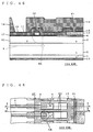
- Fig. 69 is a plan view showing a gate wiring region of a MOSFET having a trench gate according to the prior art. Moreover, Figs. 70 and 71 are sectional views taken along cutting lines A - A and B - B in Fig. 69, respectively. In a
device 150, an n - typeepitaxial layer 72 is formed on an n -type substrate layer 71 including an n - type impurity having a high concentration and has a lower impurity concentration than in the n -type substrate layer 71. By these semiconductor layers, asemiconductor substrate 99 is constituted. - A p -
type semiconductor layer 96 anda p well layer 73 are selectively formed in a surface of the n - typeepitaxial layer 72, that is, an upper main surface of thesemiconductor substrate 99. Thep well layer 73 is formed to be connected to the p -type semiconductor layer 96, and furthermore, to surround a periphery of the p -type semiconductor layer 96. - A plurality of
gate trenches 76 arranged in parallel with each other are formed like a band in the upper main surface of thesemiconductor substrate 99. Thegate trench 76 is formed more deeply than the p -type semiconductor layer 96 and more shallowly than the n - typeepitaxial layer 72. In the gate wiring region shown in Figs. 69 to 71, an edge of thegate trench 76 along its longitudinal direction is present. An internal wall of thegate trench 76 is covered with agate insulating film 78. Agate electrode 77 made of polysilicon doped with an impurity having a high concentration is buried in thegate trench 76 through thegate insulating film 78. - In the gate wiring region, an area in the upper main surface of the
semiconductor substrate 99 where agate electrode 7 is not present is covered with aninsulating film 87 or aninsulating film 74. Theinsulating film 74 is selectively formed as a LOCOS (local oxidation of silicon) film more thickly than theinsulating film 87 in a direction of an array ofgate trenches 6 over thep well layer 73 while keeping a space with thegate trench 6. In the vicinity of an end of thegate trench 6 along its longitudinal direction, thegate electrode 77 is connected to agate wiring 79. - The
gate wiring 79 is formed of the same material as a material of thegate electrode 77, and furthermore, is continuously provided integrally with thegate electrode 77. Moreover, thegate wiring 79 is provided on theinsulating film 74 and is extended toward thegate trench 6 to cover an edge portion of thegate electrode 77 in order to implement a connection with thegate electrode 77. Theinsulating film 74 is provided to keep a high breakdown voltage between thegate wiring 79 and thep well layer 73. - Furthermore, an n -
type semiconductor layer 75 containing arsenic in a high concentration is selectively formed in the upper main surface of thesemiconductor substrate 99. The n -type semiconductor layer 75 is formed to surround an upper end UE of an edge of thegate trench 6 along its longitudinal direction. In a process of manufacturing the device, the n -type semiconductor layer 75 is formed, and thegate trench 76 and theinsulating film 87 are then formed by a thermal oxidation treatment. At this time, the oxidation is accelerated by the action of the impurity contained in the n -type semiconductor layer 75. Therefore, thegate trench 76 and theinsulating film 87 which cover the vicinity of the upper end UE are completed thickly. Consequently, it is possible to obtain the effect of increasing insulation strengths of thegate electrode 77 and theinsulating film 87 in the vicinity of the upper end UE. - The surfaces of the
gate electrode 77 and thegate wiring 79 are covered with an insulator having a three-layer structure constituted by aninsulating film 86, aBPSG layer 81 and aninsulating film 89. Both of theinsulating films source electrode 84 and agate wiring 83 are provided on theinsulating film 89. Both thesource electrode 84 and thegate wiring 83 are made of Al - Si. In the insulator having the three - layer structure, anopening 95 is selectively formed in a portion provided above theinsulating film 74, and thegate wiring 79 and thegate wiring 83 are electrically connected through the opening 95. Adrain electrode 85 is provided on a lower main surface of thesemiconductor substrate 99, that is, a surface of the n -type substrate layer 71. - An n-type source layer is selectively formed in an area in the upper main surface of the
semiconductor substrate 99 which is provided adjacently to thegate trench 76 over the cell region of the device, which is not shown. Thesource electrode 84 is connected to the n - typeepitaxial layer 72 and the n - type source layer which are exposed to the upper main surface of thesemiconductor substrate 99 in the cell region. A portion of the p -type semiconductor layer 96 which is interposed between the n - type source layer and the n - typeepitaxial layer 72 and is opposed to thegate electrode 77 functions as a channel region. - When using the device, a positive voltage with reference to the
source electrode 84 is applied to thedrain electrode 85. By regulating a voltage to be applied to thegate electrode 77 through thegate wiring 83 and thegate wiring 79, a magnitude of the main current flowing from thedrain electrode 85 to thesource electrode 84 is controlled. - In order to make the
drain electrode 85 and thesource electrode 84 conductive, a positive gate voltage for thesource electrode 84 is applied to thegate electrode 77. Since thegate electrode 77 and thegate wiring 79 are connected to each other, their electric potentials are equal to each other. Moreover, since thep well layer 73 and thesource electrode 14 are connected to each other, their electric potentials are also equal to each other. For this reason, when the device is set in a conducting state, an electric field E having a magnitude ofgate insulating film 78 and theinsulating film 87 which are provided between thegate electrode 77 andgate wiring 79, and thep well layer 73. - In order to bring the device into a cut-off state, a zero or negative voltage is applied as a gate voltage. When the gate voltage is zero, the electric field E generated in the insulating film is set to E = 0. In other words, the electric field in the insulating film disappears. When the gate voltage has a negative value (- VGS), the electric field E having a magnitude of
- By taking a well-known HTGB (high temperature gate bias) test as an example, the
device 150 as a test object is kept in a high-temperature state by using a thermostat or a hot plate. With this state kept and thesource electrode 84 and thedrain electrode 85 short-circuited through an external wiring, a gate voltage is applied between thegate electrode 77 and thesource electrode 14. Both positive and negative voltages are applied as the gate voltage. - In addition, a magnitude of the gate voltage to be applied is set to approximate to an assured actual value for the
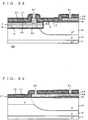
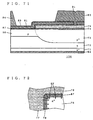
device 150 in many cases. Thedevice 150 is put under such severe conditions for a long period of time. For that period, the situation of a deterioration in thegate insulating film 78 and theinsulating film 87 and a degree of a change in other characteristics are investigated. Through such tests, a portion covering the upper end UE of thegate trench 6 described above is indicated as one of weak portions of the insulating film. - The upper end UE is a portion where the
semiconductor layer 75 is protruded at a right angle toward thegate electrode 77 and thegate wiring 79 as is enlarged in Fig. 72. For this reason, an electric field EF concentrates in the portion covering the upper end UE in thegate insulating film 78 and theinsulating film 87. In addition, thegate insulating film 78 and the insulatingfilm 87 are sharply bent at the upper end UE. Therefore, the film tends to have a small thickness. More specifically, the portion covering the upper end UE in thegate insulating film 78 and the insulatingfilm 87 is a weak portion in a double sense with regard to an increase in the gate breakdown voltage (gate - source breakdown voltage) of the device. - The n -
type semiconductor layer 75 is provided in order to improve the weak portion by increasing the thickness of the insulating film covering the upper end UE. In order to produce the effect of so-called "enhanced oxidation" by the arsenic contained in the n -type semiconductor layer 75, however, it is necessary to keep a time for a heat treatment to form the insulatingfilms gate insulating film 78 other than the upper end UE also become considerably thick. Consequently, a gate threshold voltage is dropped, and furthermore, an ON - state resistance is increased. For this reason, a device capable of producing the effect of thegate insulating film 78 is restricted to a device in which a low voltage is applied to a gate or a device in which the time for the heat treatment to form the insulatingfilms - In the conventional insulated gate semiconductor device, thus, a portion having a small insulation strength is present on the insulating film related to the insulation of the gate electrode and the gate wiring. Therefore, there has been a problem in that a reliability of the insulating film is poor and is also reflected in a yield of the device as a product.
- In order to solve the above-mentioned problems, it is an object of the present invention to provide an insulated gate semiconductor device capable of enhancing an insulation strength, that is, a gate breakdown voltage and a reliability of an insulating film related to insulation of a gate electrode and a gate wiring, thereby improving a yield of a product, and furthermore, to provide a method suitable for manufacture of the insulated gate semiconductor device.
- A first aspect of the present invention is directed to an insulated gate semiconductor device comprising a semiconductor substrate defining an upper main surface and a lower main surface, the semiconductor substrate including a first semiconductor layer of a first conductivity type which is exposed to the upper main surface, a second semiconductor layer of a second conductivity type which is selectively formed in a portion of the upper main surface in the first semiconductor layer, and a third semiconductor layer of the first conductivity type which is selectively formed in a portion of the upper main surface in the second semiconductor layer and has a higher impurity concentration than an impurity concentration in the first semiconductor layer, wherein the semiconductor substrate is provided with a trench opened on the upper main surface and reaching the first semiconductor layer through the third and second semiconductor layers.
- Moreover, the device further comprises an insulating film covering an internal wall of the trench and the upper main surface, a gate electrode buried in the trench through the insulating film, a first gate wiring which is selectively provided both on the gate electrode apart from an edge of the trench along its longitudinal direction and on the insulating film covering the upper main surface, is made of the same material as a material of the gate electrode and is continuously provided integrally with the gate electrode, a second gate wiring which is provided over the upper main surface through the insulating film opposite to the first gate wiring apart from the edge of the trench and is made of the same material as the material of the gate electrode, a third gate wiring for electrically connecting the first gate wiring and the second gate wiring, and a pair of main electrodes which are electrically connected to a surface of the semiconductor substrate, respectively.
- The third gate wiring is provided apart from the edge of the trench, one of the pair of main electrodes is electrically connected to the second and third semiconductor layers on the upper main surface, and an upper surface of the gate electrode is positioned on the same plane with the upper main surface or therebelow in a portion which is in contact with the edge of the trench.
- A second aspect of the present invention is directed to the insulated gate semiconductor device according to the first aspect of the present invention, further comprising an insulating layer covering the first and second gate wirings and having a first opening and a second opening selectively formed on the first and second gate wirings, respectively, wherein the third gate wiring includes a connecting wiring formed on the insulating layer and electrically connecting the first gate wiring and the second gate wiring through the first and second openings.
- A third aspect of the present invention is directed to the insulated gate semiconductor device according to the second aspect of the present invention, wherein the trench is divided into a plurality of unit trenches arranged in parallel with each other, and the first gate wiring is provided like a band to intersect the unit trenches.
- A fourth aspect of the present invention is directed to the insulated gate semiconductor device according to the third aspect of the present invention, wherein the first opening is formed like a band in a longitudinal direction of the first gate wiring.
- A fifth aspect of the present invention is directed to the insulated gate semiconductor device according to the third aspect of the present invention, wherein the first opening is dispersively formed to keep away from portions above the unit trenches.
- A sixth aspect of the present invention is directed to the insulated gate semiconductor device according to the third aspect of the present invention, wherein the first opening is dispersively formed by selecting portions above the unit trenches.
- A seventh aspect of the present invention is directed to the insulated gate semiconductor device according to the first aspect of the present invention, wherein the third gate wiring includes a connecting wiring which is provided over the upper main surface through the insulating film, is made of the same material as materials of the first and second gate wirings, and is continuously provided integrally with the first and second gate wirings.
- An eighth aspect of the present invention is directed to the insulated gate semiconductor device according to the seventh aspect of the present invention, further comprising an insulating layer covering the first and second gate wirings and having a first opening and a second opening selectively formed on the first and second gate wirings, respectively, wherein the third gate wiring further includes another connecting wiring formed on the insulating layer and electrically connecting the first gate wiring and the second gate wiring through the first and second openings.
- A ninth aspect of the present invention is directed to the insulated gate semiconductor device according to the seventh aspect of the present invention, wherein the trench is divided into a plurality of unit trenches arranged in parallel with each other, the first gate wiring is provided like a band to intersect the unit trenches, and the connecting wiring is provided along a region interposed between the unit trenches in the upper main surface.
- A tenth aspect of the present invention is directed to the insulated gate semiconductor device according to the first aspect of the present invention, wherein the insulating film covering the upper main surface of the semiconductor substrate is formed as a tick insulating film more thickly in a region directly under the second gate wiring than in other regions.
- An eleventh aspect of the present invention is directed to the insulated gate semiconductor device according to the tenth aspect of the present invention, wherein the semiconductor substrate further includes a high concentration semiconductor layer of a first conductivity type which is selectively formed in the upper main surface to surround an upper end of the edge of the trench and has a higher impurity concentration than an impurity concentration in the first semiconductor layer, the high concentration semiconductor layer being also formed to cover a portion directly under an edge of the thick insulating film.
- A twelfth aspect of the present invention is directed to the insulated gate semiconductor device according to the first aspect of the present invention, wherein the semiconductor substrate further includes a fourth semiconductor layer of the second conductivity type which is selectively formed in a portion of the upper main surface including a region directly under the second gate wiring so as to be coupled to the second semiconductor layer and to surround a periphery thereof, the fourth semiconductor layer being deeper tan the second semiconductor layer and surrounding a lower end of the edge of the trench.
- A thirteenth aspect of the present invention is directed to the insulated gate semiconductor device according to the first aspect of the present invention, wherein the second semiconductor layer is extended to a region directly under the second gate wiring in the upper main surface.
- A fourteenth aspect of the present invention is directed to the insulated gate semiconductor device according to the first aspect of the present invention, wherein the semiconductor substrate further includes a high concentration semiconductor layer of a first conductivity type which is selectively formed in the upper main surface to surround an upper end of the edge of the trench and has a higher impurity concentration than an impurity concentration in the first semiconductor layer.
- A fifteenth aspect of the present invention is directed to the insulated gate semiconductor device according to the fourteenth aspect of the present invention, wherein the high concentration semiconductor layer is also formed to cover a region directly under the first gate wiring.
- A sixteenth aspect of the present invention is directed to a method of manufacturing an insulated gate semiconductor device comprising a step of preparing a semiconductor substrate defining an upper main surface and a lower main surface and including a first semiconductor layer of a first conductivity type which is exposed to the upper main surface, a step of selectively forming a second semiconductor layer of a second conductivity type in a portion of the upper main surface in the first semiconductor layer by selectively introducing an impurity of the second conductivity type into the upper main surface, a third semiconductor layer forming step of selectively forming a third semiconductor layer of the first conductivity type having a higher impurity concentration than an impurity concentration in the first semiconductor layer in a portion of the upper main surface in the second semiconductor layer by selectively introducing an impurity of the first conductivity type into the upper main surface, a trench forming step of selectively forming, in the semiconductor substrate, a trench reaching the first semiconductor layer through the third and second semiconductor layers by selectively performing etching on the upper main surface, a step of forming an insulating film covering an internal wall of the trench and the upper main surface, a step of depositing a conductive layer to cover the insulating film, a gate forming step of, by selectively removing the conductive layer, forming a gate electrode buried in the trench through the insulating film, a first gate wiring which is selectively provided both on the gate electrode apart from an edge of the trench along its longitudinal direction and on the insulating film covering the upper main surface and is continuously provided integrally with the gate electrode, and a second gate wiring provided over the upper main surface through the insulating film opposite to the first gate wiring apart from the edge of the trench, a step of depositing an insulating layer to cover the first and second gate wirings, a step of selectively forming a first opening and a second opening over the first and second gate wirings in the insulating layer, respectively, a step of forming a connecting wiring which electrically connects the first gate wiring and the second gate wiring by covering the insulating layer and filling in the first and second openings, and a main electrode forming step of forming a pair of main electrodes to be electrically connected to a surface of the semiconductor substrate, respectively.
- One of the pair of main electrodes is formed to be electrically connected to the second and third semiconductor layers on the upper main surface at the main electrode forming step, and the gate electrode is formed such that an upper surface of the gate electrode is positioned on the same plane with the upper main surface or therebelow in a portion which is in contact with the edge of the trench at the gate forming step.
- A seventeenth aspect of the present invention is directed to the method of manufacturing an insulated gate semiconductor device according to the sixteenth aspect of the present invention, further comprising a step of forming, on the upper main surface, a shielding film selectively opened prior to the trench forming step, and a step of selectively forming a thick insulating film which is thicker than the insulating film in a region where the shielding film is opened by performing a thermal oxidation treatment on the upper main surface, wherein the trench is formed to keep away from the thick insulating film at the trench forming step, and the second gate wiring is formed on the thick insulating film at the gate forming step.
- An eighteenth aspect of the present invention is directed to the method of manufacturing an insulated gate semiconductor device according to the sixteenth aspect of the present invention, further comprising a step of selectively forming, in a portion of the upper main surface of the semiconductor substrate, a high concentration semiconductor layer of a first conductivity type which has a higher impurity concentration than an impurity concentration in the first semiconductor layer by selectively introducing an impurity of the first conductivity type into the upper main surface simultaneously with the third semiconductor forming step. An upper end of the edge of the trench is formed to be surrounded by the high concentration semiconductor layer at the trench forming step.
- A nineteenth aspect of the present invention is directed to a method of manufacturing an insulated gate semiconductor device comprising a step of preparing a semiconductor substrate defining an upper main surface and a lower main surface and including a first semiconductor layer of a first conductivity type which is exposed to the upper main surface, a step of selectively forming a second semiconductor layer of a second conductivity type in a portion of the upper main surface in the first semiconductor layer by selectively introducing an impurity of the second conductivity type into the upper main surface, a third semiconductor layer forming step of selectively forming a third semiconductor layer of the first conductivity type having a higher impurity concentration than an impurity concentration in the first semiconductor layer in a portion of the upper main surface in the second semiconductor layer by selectively introducing an impurity of the first conductivity type into the upper main surface, a trench forming step of selectively forming, in the semiconductor substrate, a trench reaching the first semiconductor layer through the third and second semiconductor layers by selectively performing etching on the upper main surface, a step of forming an insulating film covering an internal wall of the trench and the upper main surface, a step of depositing a conductive layer to cover the insulating film, a gate forming step of, by selectively removing the conductive layer, forming a gate electrode buried in the trench through the insulating film, a first gate wiring which is selectively provided both on the gate electrode apart from an edge of the trench along its longitudinal direction and on the insulating film covering the upper main surface and is continuously provided integrally with the gate electrode, a second gate wiring provided over the upper main surface through the insulating film opposite to the first gate wiring apart from the edge of the trench, and a connecting wiring provided over the upper main surface through the insulating film apart from the edge of the trench and continuously provided integrally with the first and second gate wirings, and a main electrode forming step of forming a pair of main electrodes to be electrically connected to a surface of the semiconductor substrate, respectively.
- One of the pair of main electrodes is formed to be electrically connected to the second and third semiconductor layers on the upper main surface at the main electrode forming step, and the gate electrode is formed such that an upper surface of the gate electrode is positioned on the same plane with the upper main surface or therebelow in a portion which is in contact with the edge of the trench at the gate forming step.
- A twentieth aspect of the present invention is directed to the method of manufacturing an insulated gate semiconductor device according to the nineteenth aspect of the present invention, further comprising a step of depositing an insulating layer to cover the first and second gate wirings, a step of selectively forming a first opening and a second opening over the first and second gate wirings in the insulating layer, respectively, and a step of forming another connecting wiring which electrically connects the first gate wiring and the second gate wiring by covering the insulating layer and filling in the first and second openings.
- In the device according to the first aspect, all the first to third gate wirings and the gate electrode are provided apart from the insulating film covering the upper end of the edge of the trench along its longitudinal direction. Consequently, a concentration of an electric field generated in the insulating film covering the upper end of the trench by a gate voltage applied to the gate electrode and the gate wiring can be relieved or eliminated. Thus, the gate breakdown voltage and yield of the device can be enhanced.
- In the device according to the second aspect, the first and second gate wirings are connected to each other through the connecting wiring formed on the first and second gate wirings. Consequently, it is not necessary to match relative positions between the connecting wiring and the trench with high precision. Therefore, manufacture can easily be performed.
- In the device according to the third aspect, the trench is divided into a plurality of unit trenches. Therefore, a density of a main current can be increased. Moreover, the first gate wiring is provided like a band to intersect the unit trenches, and therefore, alignment of the first gate wiring in a direction of an array of the unit trenches does not require high precision. Therefore, the manufacture can easily be performed.
- In the device according to the fourth aspect, the first opening is formed like a band in a longitudinal direction of the band-shaped first gate wiring, and therefore, high precision is not required for the position of the first opening. Therefore, the manufacture can easily be performed.
- In the device according to the fifth aspect, the first opening is dispersively formed. Therefore, when the first opening is formed, the influence on the insulating film positioned directly under the first gate wiring can be comparatively reduced. Consequently, a comparatively high reliability can be obtained for the portion of the insulating film positioned directly under the first gate wiring. Moreover, a comparatively large flat portion on the upper surface of the insulating layer is selected to form the first opening by keeping away from the portions above the unit trenches. Accordingly, the first opening can be formed comparatively easily.
- In the device according to the sixth aspect, the first opening is formed by selecting the portions above the unit trenches. Therefore, when the first opening is formed, the insulating film positioned directly under the first gate wiring is not affected. Consequently, a high reliability can be obtained for the portion of the insulating film positioned directly under the first gate wiring.
- In the device according to the seventh aspect, the first and second gate wirings are connected to each other through the connecting wiring which is made of the same material as the materials of the first and second gate wirings and is continuously provided integrally with the first and second gate wirings. Therefore, an electric resistance between the first and second gate wirings can be reduced. Consequently, a switching speed of the device can be increased.
- In the device according to the eighth aspect, the first and second gate wirings are further connected to each other through another connecting wiring. Therefore, the electric resistance between the first and second gate wirings can further be reduced. Consequently, the switching speed of the device can be increased still more.
- In the device according to the ninth aspect, the trench is divided into a plurality of unit trenches. Therefore, the density of the main current can be increased. Moreover, the connecting wiring is provided along a region interposed between the unit trenches in the upper main surface, that is, a region close to the gate electrode. Therefore, an electric resistance between the gate electrode and the second gate wiring can be reduced.
- In the device according to the tenth aspect, the thick insulating film is inserted between the second gate wiring and the semiconductor substrate. Therefore, an insulation strength between the second gate wiring and the semiconductor substrate can be kept high.
- In the device according to the eleventh aspect, the upper end of the edge of the trench is surrounded by the high concentration semiconductor layer. Therefore, the insulating film covering the upper end is formed thickly. Moreover, the high concentration semiconductor layer is also formed directly under the edge of the thick insulating film which is a weak portion of the insulating film. Therefore, the weak portion is reinforced. As a result, the reliability of the insulating film can be enhanced.
- In the device according to the twelfth aspect, the fourth semiconductor layer is formed to surround the periphery of the second semiconductor layer and the lower end of the edge of the trench. Therefore, the breakdown voltage of the device can be enhanced.
- In the device according to the thirteenth aspect, the second semiconductor layer is extended to the region directly under the second gate wiring. Therefore, it is possible to obtain a comparatively high breakdown voltage without providing the fourth semiconductor layer separately.
- In the device according to the fourteenth aspect, the upper end of the edge of the trench is surrounded by the high concentration semiconductor layer. Therefore, the insulating film covering the upper end is formed thickly. Consequently, the reliability of the insulating film can be enhanced.
- In the device according to the fifteenth aspect, the high concentration semiconductor layer is also formed to cover the region directly under the first gate wiring. Therefore, it is possible to compensate for a deterioration in the insulating layer provided directly under the first gate wiring which is caused when forming the opening of the insulating layer over the first gate wiring. In other words, the reliability of the insulating layer can be enhanced.
- In the manufacturing method according to the sixteenth aspect, a device capable of relieving or eliminating the concentration of the electric field generated on the insulating film covering the upper end of the trench can easily be manufactured by a combination of conventionally well - known techniques. In addition, the first and second gate wirings are connected to each other through the connecting wiring formed on the first and second gate wirings. Therefore, it is not necessary to match relative positions between the connecting wiring and the trench with high precision. Consequently, the manufacture can particularly be performed easily.
- In the manufacturing method according to the seventeenth aspect, it is possible to easily manufacture a device having a high insulation strength between the second gate wiring and the semiconductor substrate.
- In the manufacturing method according to the eighteenth aspect, it is possible to easily manufacture a device having a high reliability of the insulating film.
- In the manufacturing method according to the nineteenth aspect, the concentration of the electric field generated in the insulating film covering the upper end of the trench can be relieved or eliminated. In addition, it is possible to easily manufacture a device having a high switching speed by the combination of the conventionally well - known techniques.
- In the manufacturing method according to the twentieth aspect, it is possible to easily manufacture a device having a higher switching speed.
- The objects, features, aspects and advantages of the present invention will become more apparent from the following detailed description and the accompanying drawings.
-
- Figure 1 is a sectional front view showing a device according to a first embodiment;
- Figure 2 is a sectional plan view showing the device according to the first embodiment;
- Figure 3 is a plan view showing the device according to the first embodiment;
- Figure 4 is a sectional front view showing the device according to the first embodiment;
- Figure 5 is a sectional side view showing the device according to the first embodiment;
- Figure 6 is an enlarged sectional front view showing the device according to the first embodiment;
- Figure 7 is a sectional plan view showing another example of the device according to the first embodiment;
- Figures 8 to 36 are views showing a process of manufacturing the device according to the first embodiment;
- Figure 37 is a plan view showing a device according to a second embodiment;
- Figure 38 is a sectional front view showing the device according to the second embodiment;
- Figure 39 is a sectional side view showing the device according to the second embodiment;
- Figure 40 is a plan view showing another example of the device according to the second embodiment;
- Figure 41 is a plan view showing a device according to a third embodiment;
- Figures 42 and 43 are sectional front views showing the device according to the third embodiment;
- Figure 44 is a plan view showing another example of the device according to the third embodiment;
- Figure 45 is a sectional front view showing a device according to a fourth embodiment;
- Figure 46 is a plan view showing a device according to a fifth embodiment;
- Figures 47 and 48 are sectional front views showing the device according to the fifth embodiment;
- Figures 49 to 60 are views showing a process of manufacturing the device according to the fifth embodiment;
- Figure 61 is a plan view showing a device according to a sixth embodiment;
- Figures 62 and 63 are sectional front views showing the device according to the sixth embodiment;
- Figure 64 is a sectional front view showing a device according to a seventh embodiment;
- Figure 65 is a plan view showing a device according to an eighth embodiment;
- Figure 66 is a sectional front view showing the device according to the eighth embodiment;
- Figure 67 is a plan view showing another example of the device according to the eighth embodiment;
- Figure 68 is a sectional front view showing yet another example of the device according to the eighth embodiment;
- Figure 69 is a plan view showing a device according to the prior art;
- Figures 70 and 71 are sectional front views showing the device according to the prior art; and
- Figure 72 is an enlarged sectional front view showing the device according to the prior art.
-
- First of all, a semiconductor device according to a first embodiment will be described below.
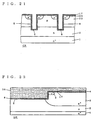
- Fig. 2 is a sectional plan view showing an upper main surface of a semiconductor substrate provided in the semiconductor device according to the first embodiment. A
device 101 is constituted as a trench type MOSFET having a large number of unit cells. Asemiconductor substrate 90 is in the shape of a plate having an upper main surface and a lower main surface, and has a large number of gate trenches (trenches) 6 formed like stripes such that they are arranged in parallel with each other along the upper main surface. Onegate trench 6 is formed for each unit cell. - A central portion (a region enclosed by a dotted line in Fig. 2) of the
semiconductor substrate 90 in which the unit cells are arranged will be referred to as a "cell region CR". A gate wiring which is not shown is provided around the cell region CR. The region where the gate wiring is provided will be referred to as a "gate wiring region GR". A sectional plan view shown in Fig. 2 is common to devices according to all embodiments which will be described below as well as thedevice 101 according to the first embodiment. - Fig. 3 is a plan view showing the
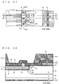
device 101 in the gate wiring region GR. Moreover, Fig. 1 is a sectional view taken along a cutting line A - A shown in Figs. 2 and 3, and Fig. 4 is a sectional view taken along a cutting line B - B. Furthermore, Fig. 5 is a sectional view taken along a cutting line C - C in Fig. 2. More specifically, Figs. 1, 3 and 4 show a structure of thedevice 101 in the gate wiring region GR, and Fig. 5 shows a structure in the cell region CR. The structure and operation of thedevice 101 will be described below with reference to these drawings. - The
semiconductor substrate 90 containing silicon as a base material is provided with a plate-shaped n -type substrate layer 1 exposed to the lower main surface and a plate-shaped n -type epitaxial layer 2 formed on the n -type substrate layer 1. A p -type semiconductor layer 22 anda p well layer 3 are selectively formed in the upper main surface of thesemiconductor substrate 90, that is, a surface of the n -type epitaxial layer 2, respectively. The n -type substrate layer 1 contains an n - type impurity in a high concentration. An impurity concentration in the n -type epitaxial layer 2 is set lower than in the n -type substrate layer 1. - The p -
type semiconductor layer 22 is formed over the whole cell region CR. Thep well layer 3 is formed to surround the p -type semiconductor layer 22 and to include a side edge of the p -type semiconductor layer 22 in the gate wiring region GR. Both the p -type semiconductor layer 22 and thep well layer 3 are shallower than the n -type epitaxial layer 2 such that their bottoms do not reach the n -type substrate layer 1. - The
gate trench 6 opened on the upper main surface of thesemiconductor substrate 90 is formed more deeply than the p -type semiconductor layer 22 and more shallowly than the n -type epitaxial layer 2. Thep well layer 3 in the gate wiring region GR is formed in order to raise a breakdown voltage of the device. For this purpose, thep well layer 3 is formed such that it is not shallower than the p -type semiconductor layer 22 in order to include the side edge of the p -type semiconductor layer 22. - In order to further enhance the breakdown voltage, it is desirable that the
p well layer 3 should be deeper than the p -type semiconductor layer 22 as shown in Fig. 4 and should be formed to include a lower end BE of an edge of thegate trench 6 along its longitudinal direction as shown in Fig. 1. In the gate wiring region GR, moreover, an n -type semiconductor layer 5 is selectively formed in the upper main surface of thesemiconductor substrate 90 so as to surround an upper end UE of the edge of thegate trench 6 along its longitudinal direction. The n -type semiconductor layer 5 contains an n - type impurity in a higher concentration than an impurity concentration in the n -type epitaxial layer 2. - In the cell region CR, an n -
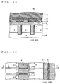
type semiconductor layer 23 is selectively formed in the upper main surface of thesemiconductor substrate 90, that is, a surface of the p -type semiconductor layer 22 adjacently to thegate trench 6. More specifically, in the cell region CR, the n -type semiconductor layer 23 and the p -type semiconductor layer 22 are selectively exposed in a region interposed between thegate trenches 6 on the upper main surface of thesemiconductor substrate 90. The n -type semiconductor layer 23 contains the n - type impurity in a higher concentration than the n -type epitaxial layer 2. Moreover, the n -type semiconductor layer 23 is formed more shallowly than the p -type semiconductor layer 22. - A
gate insulating film 8 made of silicon oxide is formed on an internal wall of thegate trench 6. Agate electrode 7 is buried in thegate trench 6 through thegate insulating film 8. Thegate electrode 7 is made of polysilicon doped with an impurity in a high concentration. An upper surface of thegate electrode 7 and a surface (Fig. 5) of a portion of thegate electrode 7 which is protruded from thegate trench 6 are covered with an insulatingfilm 16 made of silicon oxide. - Furthermore, the upper main surface of the
semiconductor substrate 90 excluding thegate trench 6 is also covered with an insulatingfilm 17 made of the silicon oxide. A part of the upper main surface in the gate wiring region GR is covered with an insulatingfilm 4 formed as a LOCOS oxide film more thickly than the insulatingfilm 17 in place of the insulatingfilm 17. As shown in Fig. 5, moreover, an opening is selectively formed in the insulatingfilm 17 in the cell region CR, and asource electrode 14 is connected to both the p -type semiconductor layer 22 and the n -type semiconductor layer 23 through the opening. - A
drain electrode 15 is formed on an exposed surface of the n -type substrate layer 1, that is, the lower main surface of thesemiconductor substrate 90. A drain current (a main current) flows through thesource electrode 14 and thedrain electrode 15. More specifically, thesource electrode 14 and thedrain electrode 15 function as a pair of main electrodes. Thesource electrode 14 is formed of Al - Si, for example and thedrain electrode 15 is formed of a Ti / Ni / Au alloy, for example. - As shown in Fig. 5, a portion of the p -
type semiconductor layer 22 which is interposed between the n -type semiconductor layer 23 and the n -type epitaxial layer 2 opposite to thegate electrode 7 through thegate insulating film 8 functions as a channel region CH. By a voltage applied to thegate electrode 7, a magnitude of the main current is controlled. In other words, thedevice 101 is constituted as an n channel type MOSFET. - Two kinds of
gate wirings gate electrode 7. Thegate wiring 9 is provided across an upper surface of thegate electrodes 7 in the vicinity of the edges of a string of thegate trenches 6 along their longitudinal direction and the upper main surface of thesemiconductor substrate 90 in a direction of an array of thegate trenches 6. In addition, thegate wiring 9 is coupled integrally with the string of thegate electrodes 7. Moreover, thegate wiring 9 is preferably formed like a band to be orthogonal to the string of thegate electrodes 7 as shown in Fig. 3. - As shown in Fig. 1, the
gate wiring 9 is provided in a position which somewhat retreats from the edge so as not to cover the upper ends UE of the edges of the string of thegate trenches 6 along their longitudinal direction. As shown in Fig. 6 illustrating the enlarged vicinity of the upper end UE, furthermore, the position of the upper surface of thegate electrode 7 is set on the same plane with the upper main surface of thesemiconductor substrate 90 or lower than it in at least the vicinity of the edge of thegate trench 6 along its longitudinal direction, and preferably, is set lower as shown in Fig. 1. By setting the position of the upper surface of thegate electrode 7 lower, the influence of manufacturing errors can also be eliminated. As shown in Fig. 1, moreover, the upper end UE is surrounded by the above-mentioned n -type semiconductor layer 5. - The insulating
film 17 is provided between the upper main surface of thesemiconductor substrate 90 and thegate wiring 9, and the two are electrically insulated by the insulatingfilm 17. In a region extending from the edge of thegate trench 6 along the longitudinal direction, an insulatingfilm 4 is formed on the exposed surface of thep well layer 3. Agate wiring 10 is provided on the insulatingfilm 4 in a direction of the array of thegate electrodes 7. Thegate wiring 10 and thep well layer 3 are electrically insulated by the insulatingfilm 4. Moreover, surfaces of thegate wirings film 18 made of a silicon oxide film in the same manner as the insulatingfilm 16 covering the upper face of thegate electrode 7. - A BPSG (silicate glass containing boron and phosphorus)
layer 11 is formed on the insulatingfilms semiconductor substrate 90, thegate electrode 7, and thegate wirings BPSG layer 11 is covered with an insulatingfilm 19 formed of a silicon oxide film. An opening is selectively formed on a multilayered insulator constituted by the insulatingfilm 18, theBPSG layer 11 and the insulatingfilm 19 in a connecting portion of thesource electrode 14 and thesemiconductor substrate 90. Consequently, a connection between thesource electrode 14 and thesemiconductor substrate 90 is implemented. - The above-mentioned multilayered insulator is further provided with an
opening 20 formed like a band along the upper surface of thegate wiring 9 and anopening 21 formed like a band along the upper surface of thegate wiring 10. Agate wiring 13 is formed on the multilayered insulator to fill in both of theopenings gate wiring 13 electrically connects thegate wiring 9 and thegate wiring 10 to each other through theopenings gate wiring 13 is formed of the same material as a material of thesource electrode 14 differently from thegate wirings gate wiring 13 and thesource electrode 14 are electrically insulated from each other. - In order to use the
device 101, first of all, an external power source which is not shown is connected. Consequently, a positive voltage is applied to thedrain electrode 15 with reference to thesource electrode 14. Usually, a load which is not shown is inserted between the external power source and thedrain electrode 15, for example. In this state, a magnitude of the main current is controlled by regulating a voltage to be applied to thegate electrode 7 through thegate wirings - With reference to the
source electrode 14, a positive gate voltage which exceeds a predetermined gate threshold voltage is applied to the gate electrode 7 (a gate is turned ON), whereby an n - type inversion layer is formed in a p - type channel region CH. As a result, the channel region CH is brought into a conducting state. Therefore, the main current flows from thedrain electrode 15 to thesource electrode 14. In other words, thedevice 101 is brought into the conducting state. - Next, when the gate voltage to be applied between the
source electrode 14 and thegate electrode 7 is returned to zero or a negative (reverse bias) value (the gate is turned OFF), the inversion layer formed in the channel region CH disappears and the channel region CH returns to an original p conductivity type. As a result, the main current does not flow between thesource electrode 14 and thedrain electrode 15. In other words, thedevice 101 is brought into a cut-off state (an OFF state). - In the
device 101, the upper end UE of thegate trench 6 is covered with neither thegate electrode 7 nor thegate wiring 9. The upper surface of thegate electrode 7 is not positioned higher than the upper main surface of thesemiconductor substrate 90 in the upper end UE, and thegate wiring 9 is provided apart from the upper end UE. A connection between thegate wiring 9 and thegate wiring 10 is implemented by thegate wiring 13 provided on the multilayered insulator including theBPSG layer 11. In other words, the gate wiring is provided to keep away from the upper end UE differently from theconventional device 150. - As a result, a concentration of an electric field generated in the
gate insulating film 8 and the insulatingfilm 17 at the upper end UE due to the gate voltage to be applied to thegate electrode 7 and thegate wirings device 101 and a yield of a product can be enhanced. - Since the upper end UE is surrounded by the n -
type semiconductor layer 5, thegate insulating film 8 and the insulatingfilm 17 at the upper end UE are formed thickly. Furthermore, the insulatingfilm 4 which is formed more thickly than the insulatingfilm 17 is inserted between thegate wiring 10 and thep well layer 3. Therefore, a sufficiently high insulation strength can be obtained between thegate wiring 10 and thep well layer 3. These also contribute to an enhancement in the breakdown voltage and reliability of the device. - While Fig. 2 shows the example in which the string of the
gate trenches 6 is arranged like bands (stripes) parallel with each other, it is sufficient that the structure of the gate wiring region GR has a configuration shown in each of Figs. 1 to 4 and Fig. 6 and the structure of the cell region CR has a configuration shown in Fig. 5. As shown in Fig. 7, for example, thegate trenches 6 may be arranged like a grid (cross stripes). Also in a device 101a, sectional structures taken along cutting lines A - A, B - B and C - C in Fig. 7 are the same as the structures shown in Figs. 1 to 6. - Figs. 8 to 37 are views showing a manufacturing process of a preferable method for manufacturing the
device 101. In order to manufacture thedevice 101, a step shown in Fig. 8 is first executed. At the step shown in Fig. 8, first of all, a semiconductor substrate containing silicon as a base material and an n - type impurity in a high concentration is prepared. The semiconductor substrate is equivalent to the above-mentioned n -type substrate layer 1. Next, an n -type epitaxial layer 2 is formed on an upper main surface of the n -type substrate layer 1 by using an epitaxial growth method. As a result, a plate-shapedsemiconductor substrate 90 containing the silicon as the base material is completed. - At a step shown in Fig. 9, subsequently, a
thermal oxide film 32 is first formed on the whole upper main surface of thesemiconductor substrate 90. Next, a portion in thethermal oxide film 32 which corresponds to thep well layer 3 is selectively removed. Furthermore, a newthermal oxide film 31 is formed more thinly than thethermal oxide film 32 in the removed region. The selective removal of thethermal oxide film 32 is executed by selective etching using, as a shield, a resist pattern formed by utilizing photolithography. This technique has conventionally be well-known. - Subsequently, boron is implanted into a surface of the n -
type epitaxial layer 2, that is, the upper main surface of thesemiconductor substrate 90 by using the patternedthermal oxide film 32 as the shield. Then, the boron is diffused by a thermal treatment. As a result,a p well layer 3 is selectively formed on an upper main surface of the n -type epitaxial layer 2. It is obvious that the diffusing step is executed incidentally to the implanting step, which will be omitted in the following description. - At a step shown in Fig. 10, first of all, a resist layer is deposited on the
thermal oxide films type semiconductor layer 22 is selectively removed, thereby forming a resistpattern 33. Next, etching is performed by using the resistpattern 33 as a shield. Consequently, thethermal oxide films - At a step shown in Fig. 11, first of all, boron is implanted into the upper main surface of the
semiconductor substrate 90, that is, a surface of the n -type epitaxial layer 2. As a result, the p -type semiconductor layer 22 is formed on the surface of the n -type epitaxial layer 2 to be connected to thep well layer 3. Then, the resistpattern 33 is removed. Thereafter, the remainingthermal oxide film 31 is removed. - At a step shown in Fig. 12, first of all, a nitride film is formed on the whole upper main surface of the
semiconductor substrate 90. Then, the nitride film is selectively removed in a region where an insulatingfilm 4 is to be formed. As a result, a patternednitride film 34 is formed. By executing a thermal oxidation treatment using thenitride film 34 as a shield, an insulatingfilm 4 is selectively formed on an opening of thenitride film 34. - Subsequently, a step shown in Figs. 13, 14 and 15 are executed. Fig. 13 is a sectional view taken along a cutting line A - A of the gate wiring region GR, and Fig. 14 is a sectional view taken along a cutting line B - B of the gate wiring region GR. Moreover, Fig. 15 is a sectional view taken along a cutting line C - C of the cell region CR.
- At this step, first of all, the
nitride film 34 is removed and athermal oxide film 91 is then formed. As a result, the upper main surface of thesemiconductor substrate 90 is covered with the insulatingfilm 4 and thethermal oxide film 91. Next, a resist layer is deposited on upper surfaces of the insulatingfilm 4 and thethermal oxide film 91, and an opening is then formed in portions corresponding to an n -type semiconductor layer 23 and an n -type semiconductor layer 5. Then, a wet etching treatment is executed using a patterned resistlayer 35 as a shield, thereby selectively removing thethermal oxide film 91. - Subsequently, arsenic is selectively implanted into the upper main surface of the
semiconductor substrate 90 using the insulatingfilm 4 and the patternedthermal oxide film 91 as shields. As a result, the n - type semiconductor layers 23 and 5 are selectively formed on the upper main surface of thesemiconductor substrate 90. Then, thethermal oxide film 91 is removed. - At a step of Fig. 16 (A - A section), Fig. 17 (B - B section) and Fig. 18 (C - C section), for example, a
thermal oxide film 36 and aHTO layer 37 are formed on an upper surface of the intermediate product. Next, an opening is selectively formed in portions of thethermal oxide film 36 and theHTO layer 37 which correspond to thegate trench 6. A MAG - RIE method is executed using the patternedthermal oxide film 36 andHTO layer 37 as shields, thereby forming agate trench 6 opened on the upper main surface of thesemiconductor substrate 90. - The
gate trench 6 is formed to penetrate the n -type semiconductor layer 23 and the n -type semiconductor layer 5. Accordingly, the n -type semiconductor layer 23 and the n -type semiconductor layer 5 are adjacent to a side wall of thegate trench 6. Then, thethermal oxide film 36 and theHTO layer 37 are removed. - At a step of Fig. 19 (A - A section), Fig. 20 (B - B section) and Fig. 21 (C - C section), a thermal oxidation treatment is executed, thereby forming a thermal oxide film on an internal wall of the
gate trench 6 and the upper main surface of thesemiconductor substrate 90. More specifically, agate insulating film 8 covering thegate trench 6 and an insulatingfilm 17 covering the upper main surface of thesemiconductor substrate 90 are formed. - At a step of Fig. 22 (A - A section), Fig. 23 (B - B section) and Fig. 24 (C - C section), subsequently, a
polysilicon layer 38 doped with an n - type impurity in a high concentration is deposited on the whole upper surface of the intermediate product. Thepolysilicon layer 38 fills up thegate trench 6, and furthermore, is deposited till a thickness from the upper main surface of thesemiconductor substrate 90 becomes larger than a certain extent. Thepolysilicon layer 38 is deposited by using a CVD method, for example. - At a step of Fig. 25 (A - A section), Fig. 26 (B - B section) and Fig. 27 (C - C section), first of all, a resist layer is deposited on an upper surface of the
polysilicon layer 38. Then, the resist layer is selectively removed excluding portions corresponding to agate wiring 9 and agate wiring 10. As a result, a resistpattern 39 is formed. - At steps of Fig. 28 (A - A section), Fig. 29 (B - B section) and Fig. 30 (C - C section), the
polysilicon layer 38 is subjected to selective etching using the resistpattern 39 as a shield. Consequently, agate electrode 7 and thegate wirings gate electrode 7 is not positioned higher than the upper main surface of thesemiconductor substrate 90 in the vicinity of an upper end UE. - At a step of Fig. 31 (A - A section), Fig. 32 (B - B section) and Fig. 33 (C - C section), first of all, a thermal oxide film is formed on the whole surfaces of the
gate electrode 7 and thegate wirings film 16 covering the surface of thegate electrode 7 and an insulatingfilm 18 covering surfaces of thegate wirings BPSG layer 11 is formed on the insulatingfilms film 19 is formed in a thickness of about 100 nm, for example, on theBPSG layer 11 by using the CVD method. As a result, a multilayered insulator having a three-layer structure is obtained by the insulatingfilms BPSG layer 11 and the insulatingfilm 19. - At a step of Fig. 34 (A - A section), Fig. 35 (B - B section) and Fig. 36 (C - C section), subsequently, the multilayered insulator is subjected to selective etching by using a resist pattern which is not shown. The selective etching is executed by using a wet method and a dry method. As a result,
openings source electrode 14 to thesemiconductor substrate 90 are formed on the multilayered insulator. - Then, an Al - Si layer is deposited to fill in each opening formed in the multilayered insulator and to cover an upper surface of the multilayered insulator. The Al - Si layer is deposited by using a sputtering method, for example.
- Subsequently, the Al - Si layer is subjected to patterning. Consequently, the
source electrode 14 and agate wiring 13 are formed as shown in Fig. 1 and Figs. 3 to 5. Then, adrain electrode 15 is formed on a surface of an n -type substrate layer 1, that is, a lower main surface of thesemiconductor substrate 90. Thus, thedevice 101 is completed. Thedrain electrode 15 is formed by depositing a Ti / Ni / Au alloy on the surface of the n -type substrate layer 1 by using the sputtering method, for example. - As described above, the
device 101 can easily be manufactured by combining conventionally well - known techniques such as photolithography, ion implantation, a CVD method, a thermal oxidation treatment and the like. - Fig. 37 is a plan view showing a gate wiring region GR of a
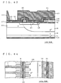
device 102 according to a second embodiment. Figs. 38 and 39 are sectional views taken along cutting lines A - A and D - D in Fig. 37, respectively. Moreover, a sectional view taken along a cutting line B - B in Fig. 37 is drawn identically to Fig. 4. As described above, furthermore, the sectional plan view of Fig. 3 is common to all the embodiments, and the cutting lines A - A and B - B shown in Fig. 37 correspond to the cutting lines A - A and B - B of Fig. 3, respectively. - The
device 102 is characteristically different from thedevice 101 according to the first embodiment in that anopening 40 formed in a portion deposited on agate wiring 9 in a multilayered insulator including aBPSG layer 11 keeps away from a portion provided above agate trench 6. More specifically, theopening 40 is not formed like a band along the band-shapedgate wiring 9 but is formed at intervals for each region interposed between theadjacent gate trenches 6. Agate wiring 13 is connected to thegate wiring 9 through theopening 40. - As shown in Fig. 39, an upper surface of the
BPSG layer 11 retreats somewhat downward in a position above thegate trench 6. More specifically, a periodic difference in height appears on the upper face of theBPSG layer 11 corresponding to an array of thegate trenches 6. Thegate trench 6 has a width of about 1 µm, for example. On the other hand, thegate trench 6 has a space of about 3 µm, for example, which is usually set greater than the width of thegate trench 6. Accordingly, a flat portion of theBPSG layer 11 is narrow above thegate trench 6, and is wide above the region interposed between thegate trenches 6. Theopening 40 is formed by selecting the wide flat portion. Therefore, alignment of a mask pattern for forming theopening 40 can be performed comparatively easily. - Moreover, a microfabrication processing is required when forming the
opening 40. Therefore, dry etching is used. For this reason, an upper surface of thegate wiring 9 is also somewhat subjected to etch-back in a portion of theopening 40 as shown in Fig. 39, and so is thegate wiring 9 provided directly under the opening 20 (Fig. 1) according to the first embodiment. Consequently, the reliability of an insulatingfilm 17 positioned directly under thegate wiring 9 is also affected. - Accordingly, it is desirable that the opening to be formed on
the-gate wiring 9 should be as narrow as possible in order to keep the reliability of thegate wiring 9 and the insulatingfilm 17. Thedevice 102 is more desirable than thedevice 101 in that theopening 40 is locally provided. - On the other hand, the position of the
opening 20 does not need to be matched with a specific flat portion on the upper face of theBPSG layer 11 in thedevice 101 according to the first embodiment. Therefore, there is an advantage that the alignment of a mask pattern for forming theopening 20 requires less precision than in theopening 40 and manufacture can easily be performed. Moreover, theopening 20 has a great opening area. Therefore, a low contact resistance is generated between thegate wiring 13 and thegate wiring 9. Consequently, good results can be obtained for a switching speed of the device. - In order to manufacture the
device 102, it is desirable that theBPSG layer 11 and the like should be selectively removed to form theopening 40 instead of forming theopening 20 at the steps of Figs. 34 to 36 in the method for manufacturing thedevice 101. For this purpose, it is sufficient that a resist pattern acting as a shield which can form theopening 20 is simply replaced with a resist pattern capable of forming theopening 40. - Fig. 40 is a plan view showing a gate wiring region GR of another
device 102a according to the second embodiment. Thedevice 102a is characteristically different from thedevice 102 in that anopening 41 to be formed in a portion of a multilayered insulator including aBPSG layer 11 which is deposited on agate wiring 9 is provided by selecting a portion above agate trench 6. More specifically, theopening 41 is selectively formed in a position of the narrower flat portion in the upper surface of theBPSG layer 11 in Fig. 39. - An opening width of the
opening 41 in a direction of an array of thegate trenches 6 is restricted. Therefore, it is desirable that the opening width of theopening 41 in a longitudinal direction of thegate trench 6 should be set large as shown in Fig. 40 in order to compensate for so-called loading effects of dry etching (a phenomenon in which an etching speed is reduced if the opening width is small). For this purpose, it is necessary to set the width of thegate wiring 9 large as shown in Fig. 40. - In the same manner as in the
device 102, in thedevice 102a, theopening 41 is not only provided locally but also formed by keeping away from a portion above an insulatingfilm 17 to select a portion above agate electrode 7. Therefore, there is an advantage that the insulatingfilm 17 can be prevented form being deteriorated due to the dry etching. - In order to manufacture the
device 102a, it is desirable that theBPSG layer 11 and the like should be selectively removed to form theopening 41 instead of forming theopening 20 at the steps of Figs. 34 to 36 in the method for manufacturing thedevice 101. For this purpose, it is sufficient that a resist pattern acting as a shield which can form theopening 20 is simply replaced with a resist pattern capable of forming theopening 41. - Fig. 41 is a plan view showing a gate wiring region GR of a
device 103 according to a third embodiment. Moreover, Figs. 42 and 43 are sectional views taken along cutting lines A - A and B - B in Fig. 41, respectively. Thedevice 103 is characteristically different from thedevice 101 according to the first embodiment in that an n -type semiconductor layer 45 is formed in place of the n -type semiconductor layer 5. - The n -
type semiconductor layer 45 formed to surround an upper end UE of agate trench 6 is extended to a position where it overlaps with an insulatingfilm 4. A connecting portion LE between an insulatingfilm 17 formed comparatively thinly and the insulatingfilm 4 formed thickly is a portion where a thermal stress remains. In some cases, moreover, the insulatingfilm 17 is formed locally thinly as compared with an average thickness in the connecting portion LE. Thus, the connecting portion LE is a weak portion of the insulatingfilm 17. In thedevice 103, the n -type semiconductor layer 45 also covers a portion directly under the connecting portion LE. Also in the connecting portion LE, therefore, the insulatingfilm 17 is formed thickly. In other words, thedevice 103 is constituted to reinforce the weak portion in the insulatingfilm 17. - Moreover, the n -
type semiconductor layer 45 is also formed without a clearance betweenadjacent gate trenches 6 to cover the whole region corresponding to a portion directly under agate wiring 9 in an upper main surface of asemiconductor substrate 90 as shown in Figs. 41 and 43. As described above, in some cases, a portion in the insulatingfilm 17 which is positioned directly under anopening 20 may be deteriorated at a dry etching step for forming theopening 20. - In the
device 103, however, a region in the insulatingfilm 17 which corresponds to the portion directly under thegate wiring 9 is covered with the n -type semiconductor layer 45. In this region, therefore, the insulatingfilm 17 is formed thickly. Consequently, it is possible to compensate for the deterioration in the insulatingfilm 17 caused by the dry etching. As shown in Fig. 41, moreover, the n -type semiconductor layer 45 is preferably formed like a band in a direction of an array of thegate trenches 6. In this configuration, alignment of a mask pattern for forming the n -type semiconductor layer 45 requires less precision. Therefore, manufacture can easily be performed. - In order to manufacture the
device 103, it is desirable that arsenic should be selectively implanted to form the n -type semiconductor layer 45 instead of forming the n -type semiconductor layer 5 at the steps of Figs. 13 to 15 in the method for manufacturing thedevice 101. For this purpose, it is preferable that patterning of a resistlayer 35 should be performed to have an opening in portions corresponding to an n -type semiconductor layer 23 and the n -type semiconductor layer 45. - Fig. 44 is a plan view showing a gate wiring region GR of another device 103a according to a third embodiment. In the device 103a, an n -
type semiconductor layer 46 is formed in place of the n -type semiconductor layer 45. The n -type semiconductor layer 46 formed to surround an upper end UE of agate trench 6 is provided so as not to wholly cover a region corresponding to a portion directly under agate wiring 9 in an upper main surface of asemiconductor substrate 90 differently from the n -type semiconductor layer 45. However, the n -type semiconductor layer 46 is also formed to cover a portion directly under a connecting portion LE in the same manner as the n -type semiconductor layer 45. Consequently, a weak portion in an insulatingfilm 17 is reinforced in the same manner as in thedevice 103. - In order to manufacture the device 103a, it is desirable that arsenic should be selectively implanted to form the n -
type semiconductor layer 46 instead of forming the n -type semiconductor layer 5 at the steps of Figs. 13 to 15 in the method for manufacturing thedevice 101. For this purpose, it is preferable that patterning of a resistlayer 35 should be executed to have an opening in portions corresponding to an n -type semiconductor layer 23 and the n -type semiconductor layer 46. - Fig. 45 is a sectional view showing a gate wiring region GR of a
device 104 according to a fourth embodiment, which is taken along a cutting line B - B (Fig. 2). Thedevice 104 is characteristically different from thedevice 101 according to the first embodiment in thata p well layer 3 is formed to have the same depth as a depth of a p -type semiconductor layer 22. For this reason, a lower end BE on an edge of agate trench 6 along its longitudinal direction is not covered with thep well layer 3 but is directly surrounded by an n -type epitaxial layer 2. - In order to keep a high breakdown voltage of the device, it is desirable that the lower end BE should be covered with the
p well layer 3 as in thedevice 101 according to the first embodiment. In thedevice 104, however, if an impurity concentration in thep well layer 3 is set equal to that in the p -type semiconductor layer 22, there is an advantage that thep well layer 3 and an n -type semiconductor layer 23 can be formed at the same time and a manufacturing process can be simplified. In this case, thep well layer 3 is identical to a p -type semiconductor layer 22 that is simply extended to a region of thep well layer 3. Thedevice 104 is suitable for applications in which a breakdown voltage to be required is not very high. - In order to manufacture the
device 104, it is preferable that the step of Fig. 9 in the method for manufacturing thedevice 101 should be omitted and the p -type semiconductor layer 22 should be enlarged up to the region of thep well layer 3 at the steps of Figs. 10 and 11. For this purpose, it is desirable that the resistlayer 33 shown in Fig. 10 should be selectively opened in regions corresponding to both the p -type semiconductor layer 22 and thep well layer 3. - Fig. 46 is a plan view showing a gate wiring region GR of a
device 105 according to a fifth embodiment. Moreover, Figs. 47 and 48 are sectional views taken along cutting lines A - A and B - B in Fig. 46, respectively. The cutting lines A - A and B - B shown in Fig. 46 correspond to the cutting lines A - A and B - B shown in Fig. 3, respectively. - The
device 105 is characteristically different from thedevice 101 according to the first embodiment in that an opening of a multilayered insulator including aBPSG layer 11 is not provided on agate wiring 9 but thegate wiring 9 and agate wiring 10 are connected to each other by agate wiring 93 provided on an upper main surface of asemiconductor substrate 90 through an insulatingfilm 17 so as to be kept away from agate trench 6. Thegate wiring 93 is formed of the same maternal as materials of thegate wirings gate wirings gate wirings gate wiring 42 which is integrally continuous. - In place of the
gate wiring 13 in thedevice 101, agate wiring 49 is formed. Thegate wiring 49 is formed of the same material as a material of asource electrode 14 in the same manner as thegate wiring 13. Thegate wiring 49 is electrically connected to thegate wiring 10 though anopening 20. - Also in the
device 104, the gate wiring is provided to be kept away from an upper end UE of thegate trench 6. Therefore, a concentration of an electric field generated on agate insulating film 8 and an insulatingfilm 17 in the upper end UE by the application of a gate voltage can be relieved or eliminated. - Consequently, a breakdown voltage of the
device 104 and a yield of a product can be enhanced. Moreover, since thegate wiring 9 is not connected to thegate wiring 10 through an opening provided in theBPSG layer 11 and the like but is continuously provided integrally with thegate wiring 10 through thegate wiring 93, it is possible to obtain an advantage that an electric resistance between thegate wiring 9 and thegate wiring 10 is low and a switching speed of the device can be enhanced. Furthermore, since an opening is not formed in an upper portion of thegate wiring 9, there is an advantage that a deterioration in the insulatingfilm 17 caused by dry etching can be avoided. - As compared with the
device 104, in thedevice 101 according to the first embodiment, alignment of a mask pattern which is required to form thegate wiring 93 and thegate trench 6 is not necessary therebetween, and therefore, there is an advantage that manufacture can easily be performed. Moreover, a connecting portion LE of an insulatingfilm 4 and the insulatingfilm 17 is not covered with thegate wiring 93. Therefore, there is an advantage that the breakdown voltage and reliability of the device can be enhanced. - In order to manufacture the
device 105, it is preferable that the steps of Figs. 8 to 24 in the method for manufacturing thedevice 101 should be executed and steps of Figs. 49 to 56 should be then executed. At the step of Fig. 49 (A - A section) and Fig. 50 (B - B section), first of all, a resist layer is deposited on an upper face of apolysilicon layer 38. Then, the resist layer is selectively removed excluding a portion corresponding to thegate wiring 42. As a result, a resistpattern 50 is formed. - At the next step of Fig. 51 (A - A section) and Fig. 52 (B - B section), the
polysilicon layer 38 is subjected to selective etching by using the resistpattern 50 as a shield. Consequently, agate electrode 7 and thegate wiring 42 are formed. At this step, the etching is controlled such that an upper surface of thegate electrode 7 is not positioned above the upper main surface of thesemiconductor substrate 90 in the vicinity of the upper end UE. - At the step of Fig. 53 (A - A section) and Fig. 54 (B - B section), subsequently, a thermal oxide film is first formed on the whole surfaces of the
gate electrode 7 and thegate wiring 42. More specifically, an insulatingfilm 16 covering a surface of thegate electrode 7 and an insulatingfilm 18 covering a surface of thegate wiring 42 are formed in thicknesses of about 20 to 30 nm, for example. Then, aBPSG layer 11 is formed on the insulatingfilms film 19 is formed in a thickness of about 100 nm, for example, on theBPSG layer 11 by using the CVD method. As a result, a multilayered insulator having a three - layer structure can be obtained by the insulatingfilms BPSG layer 11 and the insulatingfilm 19. - At the next step of Fig. 55 (A - A section) and Fig. 56 (B - B section), a multilayered insulator is subjected to selective etching by using a resist pattern which is not shown. The selective etching is executed by using a wet method and a dry method. As a result, an
opening 21 and an opening for connecting asource electrode 14 and thesemiconductor substrate 90 are formed on the multilayered insulator. - Then, an Al - Si layer is deposited to fill in each opening formed in the multilayered insulator and to cover an upper face of the multilayered insulator. The Al - Si layer is deposited by a sputtering method, for example.
- Subsequently, the Al - Si layer is subjected to patterning, thereby forming the
source electrode 14 and agate wiring 49 as shown in Figs. 47 and 48. Then, adrain electrode 15 is formed on a surface of an n -type substrate layer 1, that is, a lower main surface of thesemiconductor substrate 90. Thus, thedevice 105 is completed. Thedrain electrode 15 is formed by depositing a Ti / Ni / Au alloy on the surface of the n -type substrate layer 1 by using the sputtering method, for example. - As described above, the
device 105 can easily be manufactured by combining conventionally well - known techniques such as photolithography, ion implantation, a CVD method, a thermal oxidation treatment and the like in the same manner as in the method for manufacturing thedevice 101. - Fig. 57 is a plan view showing a gate wiring region GR of another
device 105a according to the fifth embodiment. Fig. 58 is a sectional view taken along a cutting line B - B in Fig. 57. Moreover, a sectional view taken along a cutting line A - A in Fig. 57 is represented in the same manner as Fig. 1. - The
device 105a is characteristically different from thedevice 105 in that anopening 20 is provided in aBPSG layer 11 and the like over agate wiring 9 included in agate wiring 42, and thegate wiring 9 and agate wiring 10 are connected through agate wiring 13 filling in theopenings gate wiring 93. Since thegate wiring 9 and thegate wiring 10 are connected through both thegate wiring 93 and thegate wiring 13, an electric resistance therebetween is reduced. As a result, it is possible to obtain an advantage that a switching speed of the device can be enhanced. - In order to manufacture the
device 105a, it is preferable that a step of Figs. 59 and 60 should be executed after the step of Figs. 53 and 54 in the method for manufacturing thedevice 105 are completed. At the step of Fig. 59 (A - A section) and Fig. 60 (B - B section), first of all, a multilayered insulator is subjected to selective etching by using a resist pattern which is not shown. The selective etching is executed by using a wet method and a dry method. As a result,openings source electrode 14 and asemiconductor substrate 90 are formed on the multilayered insulator. - Then, an Al - Si layer is deposited to fill in each opening formed in the multilayered insulator and to cover an upper face of the multilayered insulator. The Al - Si layer is deposited by using the sputtering method, for example.
- Subsequently, the Al - Si layer is subjected to patterning, thereby forming the
source electrode 14 and thegate wiring 13 as shown in Fig. 58. Thereafter, adrain electrode 15 is formed on a surface of an n -type substrate layer 1, that is, a lower main surface of thesemiconductor substrate 90. Thus, thedevice 101 is completed. Thedrain electrode 15 is formed by depositing a Ti / Ni / Au alloy on the surface of the n -type substrate layer 1 by using the sputtering method, for example. - Fig. 61 is a plan view showing a gate wiring region GR of a
device 106 according to a sixth embodiment. Moreover, Figs. 62 and 63 are sectional views taken along culling lines A - A and B - B in Fig. 61, respectively. In the same manner as in thedevice 103 according to the third embodiment, thedevice 106 is characteristically different from thedevice 105 according to the fifth embodiment in that an n -type semiconductor layer 45 is formed in place of the n -type semiconductor layer 5. - In the
device 106, the n -type semiconductor layer 45 also covers a portion directly under a connecting portion LE. Also in the connecting portion LE of an insulatingfilm 17 and an insulatingfilm 4, therefore, the insulatingfilm 17 is formed thickly. More specifically, thedevice 106 has an advantage that a weak portion in the insulatingfilm 17 can be reinforced. Differently from thedevice 103, the connecting portion LE is covered with agate wiring 42 in thedevice 106. Therefore, it is possible to obtain a much greater advantage by reinforcing the connecting portion LE with the n -type semiconductor layer 45. - In the same manner as in the
device 103, moreover, the n -type semiconductor layer 45 is also formed without a clearance betweenadjacent gate trenches 6 to cover the whole region corresponding to a portion provided under agate wiring 9 in an upper main surface of asemiconductor substrate 90. Therefore, it is possible to obtain an advantage that a deterioration in the insulatingfilm 17 caused by dry etching can be compensated in the region corresponding to the portion directly under thegate wiring 9. As shown in Fig. 61, moreover, the n -type semiconductor layer 45 is formed like a band in a direction of an array of thegate trenches 6. Consequently, alignment of a mask pattern can easily be performed in a manufacturing process. - In order to manufacture the
device 106, it is preferable that arsenic should be selectively implanted to form the n -type semiconductor layer 45 instead of forming the n -type semiconductor layer 5 at the steps of Figs. 13 to 15 in the method for manufacturing thedevice 101. For this purpose, it is desirable that patterning of a resistlayer 35 should be executed to have an opening in portions corresponding to an n -type semiconductor layer 23 and the n -type semiconductor layer 45. Furthermore, it is preferable that the steps of Figs. 49 to 56 according to the fifth embodiment should be executed after the steps of Figs. 8 to 24 are completed. - Fig. 64 is a sectional view showing a gate wiring region GR of a
device 107 according to a seventh embodiment, which is taken along a cutting line B - B (Fig. 2). Thedevice 107 is characteristically different from thedevice 105 according to the fifth embodiment in tat thep well layer 3 is formed to have the same depth as a depth of a p -type semiconductor layer 22 in the same manner as in thedevice 104 according to the fourth embodiment. For this reason, a lower end BE of an edge of agate trench 6 along its longitudinal direction is not covered with thep well layer 3 but is directly surrounded by an n -type epitaxial layer 2. - Also in the
device 107, the same advantages as in thedevice 104 can be obtained. More specifically, if an impurity concentration in thep well layer 3 is set equal to that of the p -type semiconductor layer 22, the p well 3 and an n -type semiconductor layer 23 can be formed at the same time. Thus, it is possible to obtain an advantage that a manufacturing process can be simplified. - In order to manufacture the
device 107, it is preferable that the step of Fig. 9 in the method for manufacturing thedevice 101 should be omitted and the p -type semiconductor layer 22 should be enlarged up to a region of thep well layer 3 at the steps of Figs. 10 and 11. For this purpose, it is desirable that the resistlayer 33 in Fig. 10 should be selectively opened in regions corresponding to both the p -type semiconductor layer 22 and thep well layer 3. Moreover, it is preferable that the steps of Figs. 49 to 56 according to the fifth embodiment should be executed after the steps of Figs. 8 to 24 are completed. - Fig. 65 is a plan view showing a gate wiring region GR of a
device 108 according to an eighth embodiment. Moreover, Fig. 66 is a sectional view taken along a cutting line A - A in Fig. 65. Thedevice 108 is characteristically different from thedevice 101 according to the first embodiment in that an n -type semiconductor layer 5 is not formed. Since the n -type semiconductor layer 5 is not formed, it is impossible to obtain an advantage that agate insulating film 8 and an insulatingfilm 17 are formed thickly in an upper end UE of agate trench 6. However, a gate wiring is provided to keep away from the upper end UE in the same manner as in thedevice 101. Therefore, it is possible to properly obtain an effect that a concentration of an electric field generated in thegate insulating film 8 and the insulatingfilm 17 at the upper end UE by the application of a gate voltage can be relieved or eliminated. - In order to manufacture the
device 108, it is preferable that arsenic should be selectively implanted such that only an n -type semiconductor layer 23 is formed and the n -type semiconductor layer 5 is not formed at the steps of Figs. 13 to 15 in the method for manufacturing thedevice 101. For this purpose, it is desirable that patterning of a resistlayer 35 should be executed to have an opening in only a portion corresponding to the n -type semiconductor layer 23. - Fig. 67 is a plan view showing a gate wiring region GR of another device 108a according to the eighth embodiment. Moreover, Fig. 68 is a sectional view taken along a cutting line A - A in Fig. 67. The device 108a is characteristically different from the
device 105 according to the fifth embodiment in that an n -type semiconductor layer 5 is not formed. Also in the device 108a, a gate wiring is provided to keep away from an upper end UE. Therefore, it is possible to properly obtain an effect that a concentration of an electric field generated in agate insulating film 8 and an insulatingfilm 17 at the upper end UE by the application of a gate voltage can be relieved or eliminated. - In order to manufacture the device 108a, it is preferable that arsenic should be selectively implanted such that only an n -
type semiconductor layer 23 is formed and the n -type semiconductor layer 5 is not formed at the steps of Figs. 13 to 15 in the method for manufacturing thedevice 101. For this purpose, it is desirable that patterning of a resistlayer 35 should be executed to have an opening in only a portion corresponding to the n -type semiconductor layer 23. Furthermore, it is preferable that the steps of Figs. 49 to 56 according to the fifth embodiment should be executed after the steps of Figs. 8 to 24 are completed. -
- (1) While an n channel type MOSFET has been taken as an example in each of the above-mentioned embodiments, the present invention can similarly be practiced and can produce the same effects for a p channel type MOSFET.
- (2) Although a so-called U - MOSFET having a U - shaped cross section
(a section taken along the cutting line C - C in Fig. 2) of the
gate trench 6 has been illustrated in each of the above-mentioned embodiments, the present invention can similarly be practiced for a so-called V - MOSFET having a V - shaped section. - (3) While the example in which the
p well layer 3 is provided has been described in each of the above-mentioned embodiments, the present invention can be carried out for a device having no p welllayer 3 with a deterioration in a breakdown voltage. Also in the device having such a structure, as long as the gate wiring is provided to keep away from the upper end UE, it is possible to properly obtain an effect that the concentration of the electric field generated in thegate insulating film 8 and the insulatingfilm 17 at the upper end UE by the application of a gate voltage can be relieved or eliminated. - (4) Although the insulating
film 4 which is thicker than the insulatingfilm 17 has been formed between thep well layer 3 and thegate wiring 10 in each of the above-mentioned embodiments, the present invention can also be carried out for a device having such a structure that an insulation of thep well layer 3 and thegate wiring 10 is kept by the insulatingfilm 17 without the formation of the insulatingfilm 4. Also in the device having such a structure, as long as the gate wiring is provided to keep away from the upper end UE, it is possible to properly obtain an effect that the concentration of the electric field generated in thegate insulating film 8 and the insulatingfilm 17 at the upper end UE by the application of the gate voltage can be relieved or eliminated. - (5) While the example in which the
source electrode 14 and thedrain electrode 15 are provided on the two main surfaces of thesemiconductor substrate 90 has been described in each of the above-mentioned embodiments, the present invention can also be practiced for a device in which both thesource electrode 14 and thedrain electrode 15 are connected to a main surface on the side where thegate trench 6 is opened. - (6) Although the MOSFET has been taken as an example in each of the
above-mentioned embodiments, the present invention can similarly be practiced for
insulated gate semiconductor devices such as an IGBT and the like other than the
MOSFET. For example, if the n -
type substrate layer 1 is replaced with a p - type substrate layer, the IGBT can be implemented. More specifically, the present invention can be practiced for a general insulated gate semiconductor device in which a gate electrode opposed to a channel region with an insulating film interposed therebetween is buried in a trench. - (7) While the example in which a plurality of
gate trenches 6 are arranged in a string has been described in each of the above-mentioned embodiments, the present invention can also be practiced for a device having asingle gate trench 6. -
- While the present invention has been described in detail, the above-mentioned description is illustrative in all aspects and the present invention is not restricted thereto. It is understood that numerous variants which are not illustrated can be supposed without departing from the scope of the invention.
Claims (20)
- An insulated gate semiconductor device comprising:a semiconductor substrate (90) defining an upper main surface and a lower main surface;said semiconductor substrate including:a first semiconductor layer (2) of a first conductivity type which is exposed to said upper main surface;a second semiconductor layer (22) of a second conductivity type which is selectively formed in a portion of said upper main surface in said first semiconductor layer; anda third semiconductor layer (23) of said first conductivity type which is selectively formed in a portion of said upper main surface in said second semiconductor layer and has a higher impurity concentration than an impurity concentration in said first semiconductor layer,
wherein said semiconductor substrate is provided with a trench (6) opened on said upper main surface and reaching said first semiconductor layer through said third and second semiconductor layers,said device further comprising:an insulating film (8, 17, 4) covering an internal wall of said trench and said upper main surface;a gate electrode (7) buried in said trench through said insulating film;a first gate wiring (9) which is selectively provided both on said gate electrode apart from an edge of said trench along its longitudinal direction and on said insulating film covering said upper main surface, is made of the same material as a material of said gate electrode and is continuously provided integrally with said gate electrode;a second gate wiring (10) which is provided over said upper main surface through said insulating film opposite to said first gate wiring apart from said edge of said trench and is made of the same material as said material of said gate electrode;a third gate wiring (13, 93) for electrically connecting said first gate wiring and said second gate wiring; anda pair of main electrodes (14, 15) which are electrically connected to a surface of said semiconductor substrate, respectively,
wherein said third gate wiring is provided apart from said edge of said trench,one of said pair of main electrodes (14) is electrically connected to said second and third semiconductor layers on said upper main surface, andan upper surface of said gate electrode is positioned on the same plane with said upper main surface or therebelow in a portion which is in contact with said edge of said trench. - The insulated gate semiconductor device according to claim 1, further comprising an insulating layer (11, 18, 19) covering said first and second gate wirings and having a first opening (20, 40, 41) and a second opening (21) selectively formed on said first and second gate wirings, respectively,
wherein said third gate wiring includes a connecting wiring (13) formed on said insulating layer and electrically connecting said first gate wiring and said second gate wiring through said first and second openings. - The insulated gate semiconductor device according to claim 2, wherein said trench is divided into a plurality of unit trenches (6) arranged in parallel with each other, andsaid first gate wiring is provided like a band to intersect said unit trenches.
- The insulated gate semiconductor device according to claim 3, wherein said first opening (20) is formed like a band in a longitudinal direction of said first gate wiring.
- The insulated gate semiconductor device according to claim 3, wherein said first opening (40) is dispersively formed to keep away from portions above said unit trenches.
- The insulated gate semiconductor device according to claim 3, wherein said first opening (41) is dispersively formed by selecting portions above said unit trenches.
- The insulated gate semiconductor device according to claim 1, wherein said third gate wiring includes a connecting wiring (93) which is provided over said upper main surface through said insulating film, is made of the same material as materials of said first and second gate wirings, and is continuously provided integrally with said first and second gate wirings.
- The insulated gate semiconductor device according to claim 7, further comprising an insulating layer (11, 18, 19) covering said first and second gate wirings and having a first opening (20, 40, 41) and a second opening (21) selectively formed on said first and second gate wirings, respectively,
wherein said third gate wiring further includes another connecting wiring (13) formed on said insulating layer and electrically connecting said first gate wiring and said second gate wiring through said first and second openings. - The insulated gate semiconductor device according to claim 7, wherein said trench is divided into a plurality of unit trenches (6) arranged in parallel with each other,said first gate wiring is provided like a band to intersect said unit trenches, andsaid connecting wiring is provided along a region interposed between said unit trenches in said upper main surface.
- The insulated gate semiconductor device according to claim 1, wherein said insulating film covering said upper main surface of said semiconductor substrate is formed as a thick insulating film (4) more thickly in a region directly under said second gate wiring than in other regions.
- The insulated gate semiconductor device according to claim 10, wherein said semiconductor substrate further includes a high concentration semiconductor layer (45, 46) of a first conductivity type which is selectively formed in said upper main surface to surround an upper end (UE) of said edge of said trench and has a higher impurity concentration than an impurity concentration in said first semiconductor layer,said high concentration semiconductor layer being also formed to cover a portion directly under an edge (LE) of said thick insulating film.
- The insulated gate semiconductor device according to claim 1, wherein said semiconductor substrate further includes a fourth semiconductor layer of said second conductivity type which is selectively formed in a portion of said upper main surface including a region directly under said second gate wiring so as to be coupled to said second semiconductor layer and to surround a periphery thereof,said fourth semiconductor layer being deeper than said second semiconductor layer and surrounding a lower end (BE) of said edge of said trench.
- The insulated gate semiconductor device according to claim 1, wherein said second semiconductor layer is extended to a region directly under said second gate wiring in said upper main surface.
- The insulated gate semiconductor device according to claim 1, wherein said semiconductor substrate further includes a high concentration semiconductor layer (5, 45, 46) of a first conductivity type which is selectively formed in said upper main surface to surround an upper end (UE) of said edge of said trench and has a higher impurity concentration than an impurity concentration in said first semiconductor layer.
- The insulated gate semiconductor device according to claim 14, wherein said high concentration semiconductor layer (5, 45) is also formed to cover a region directly under said first gate wiring.
- A method of manufacturing an insulated gate semiconductor device comprising:a step of preparing a semiconductor substrate (90) defining an upper main surface and a lower main surface and including a first semiconductor layer (2) of a first conductivity type which is exposed to said upper main surface;a step of selectively forming a second semiconductor layer (22) of a second conductivity type in a portion of said upper main surface in said first semiconductor layer by selectively introducing an impurity of said second conductivity type into said upper main surface;a third semiconductor layer forming step of selectively forming a third semiconductor layer (23) of said first conductivity type having a higher impurity concentration than an impurity concentration in said first semiconductor layer in a portion of said upper main surface in said second semiconductor layer by selectively introducing an impurity of said first conductivity type into said upper main surface;a trench forming step of selectively forming, in said semiconductor substrate, a trench (6) reaching said first semiconductor layer through said third and second semiconductor layers by selectively performing etching on said upper main surface;a step of forming an insulating film (8, 17, 4) covering an internal wall of said trench and said upper main surface;a step of depositing a conductive layer (38) to cover said insulating film;a gate forming step of, by selectively removing said conductive layer, forming a gate electrode (7) buried in said trench through said insulating film, a first gate wiring (9) which is selectively provided both on said gate electrode apart from an edge of said trench along its longitudinal direction and on said insulating film covering said upper main surface and is continuously provided integrally with said gate electrode, and a second gate wiring (10) provided over said upper main surface through said insulating film opposite to said first gate wiring apart from said edge of said trench;a step of depositing an insulating layer (11, 18, 19) to cover said first and second gate wirings;a step of selectively forming a first opening (20, 40, 41) and a second opening (21) over said first and second gate wirings in said insulating layer, respectively;a step of forming a connecting wiring (13) which electrically connects said first gate wiring and said second gate wiring by covering said insulating layer and filling in said first and second openings; anda main electrode forming step of forming a pair of main electrodes (14, 15) to be electrically connected to a surface of said semiconductor substrate, respectively,
wherein one of said pair of main electrodes (14) is formed to be electrically connected to said second and third semiconductor layers on said upper main surface at said main electrode forming step, andsaid gate electrode is formed such that an upper surface of said gate electrode is positioned on the same plane with said upper main surface or therebelow in a portion which is in contact with said edge of said trench at said gate forming step. - The method of manufacturing an insulated gate semiconductor device according to claim 16, further comprising:a step of forming, on said upper main surface, a shielding film (34) selectively opened prior to said trench forming step; anda step of selectively forming a thick insulating film which is thicker than said insulating film in a region where said shielding film is opened by performing a thermal oxidation treatment on said upper main surface,
wherein said trench is formed to keep away from said thick insulating film at said trench forming step, andsaid second gate wiring is formed on said thick insulating film at said gate forming step. - The method of manufacturing an insulated gate semiconductor device according to claim 16, further comprising:a step of selectively forming, in a portion of said upper main surface of said semiconductor substrate, a high concentration semiconductor layer (5, 45, 46) of a first conductivity type which has a higher impurity concentration than an impurity concentration in said first semiconductor layer by selectively introducing an impurity of said first conductivity type into said upper main surface simultaneously with said third semiconductor forming step,
wherein an upper end of said edge of said trench is formed to be surrounded by said high concentration semiconductor layer at said trench forming step. - A method of manufacturing an insulated gate semiconductor device comprising:a step of preparing a semiconductor substrate (90) defining an upper main surface and a lower main surface and including a first semiconductor layer (2) of a first conductivity type which is exposed to said upper main surface;a step of selectively forming a second semiconductor layer (22) of a second conductivity type in a portion of said upper main surface in said first semiconductor layer by selectively introducing an impurity of said second conductivity type into said upper main surface;a third semiconductor layer forming step of selectively forming a third semiconductor layer (23) of said first conductivity type having a higher impurity concentration than an impurity concentration in said first semiconductor layer in a portion of said upper main surface in said second semiconductor layer by selectively introducing an impurity of said first conductivity type into said upper main surface;a trench forming step of selectively forming, in said semiconductor substrate, a trench (6) reaching said first semiconductor layer through said third and second semiconductor layers by selectively performing etching on said upper main surface;a step of forming an insulating film (8, 17, 4) covering an internal wall of said trench and said upper main surface;a step of depositing a conductive layer (38) to cover said insulating film;a gate forming step of, by selectively removing said conductive layer, forming a gate electrode (7) buried in said trench through said insulating film, a first gate wiring (9) which is selectively provided both on said gate electrode apart from an edge of said trench along its longitudinal direction and on said insulating film covering said upper main surface and is continuously provided integrally with said gate electrode, a second gate wiring (10) provided over said upper main surface through said insulating film opposite to said first gate wiring apart from said edge of said trench, and a connecting wiring (93) provided over said upper main surface through said insulating film apart from said edge of said trench and continuously provided integrally with said first and second gate wirings; anda main electrode forming step of forming a pair of main electrodes (14, 15) to be electrically connected to a surface of said semiconductor substrate, respectively,
wherein one of said pair of main electrodes (14) is formed to be electrically connected to said second and third semiconductor layers on said upper main surface at said main electrode forming step, andsaid gate electrode is formed such that an upper surface of said gate electrode is positioned on the same plane with said upper main surface or therebelow in a portion which is in contact with said edge of said trench at said gate forming step. - The method of manufacturing an insulated gate semiconductor device according to claim 19, further comprising:a step of depositing an insulating layer (11, 18, 19) to cover said first and second gate wirings;a step of selectively forming a first opening (20, 40, 41) and a second opening (21) over said first and second gate wirings in said insulating layer, respectively; anda step of forming another connecting wiring (13) which electrically connects said first gate wiring and said second gate wiring by covering said insulating layer and filling in said first and second openings.
Applications Claiming Priority (1)
| Application Number | Priority Date | Filing Date | Title |
|---|---|---|---|
| PCT/JP1997/003040 WO1999012214A1 (en) | 1997-08-29 | 1997-08-29 | Insulated gate semiconductor device and method for manufacturing the same |
Publications (3)
| Publication Number | Publication Date |
|---|---|
| EP1009035A1 true EP1009035A1 (en) | 2000-06-14 |
| EP1009035A4 EP1009035A4 (en) | 2003-01-08 |
| EP1009035B1 EP1009035B1 (en) | 2004-07-21 |
Family
ID=14181048
Family Applications (1)
| Application Number | Title | Priority Date | Filing Date |
|---|---|---|---|
| EP97937855A Expired - Lifetime EP1009035B1 (en) | 1997-08-29 | 1997-08-29 | Insulated gate semiconductor device and method for manufacturing the same |
Country Status (6)
| Country | Link |
|---|---|
| US (1) | US6285058B1 (en) |
| EP (1) | EP1009035B1 (en) |
| JP (1) | JP3299283B2 (en) |
| KR (1) | KR100334445B1 (en) |
| DE (1) | DE69729963T2 (en) |
| WO (1) | WO1999012214A1 (en) |
Cited By (8)
| Publication number | Priority date | Publication date | Assignee | Title |
|---|---|---|---|---|
| WO2003021684A1 (en) * | 2001-09-04 | 2003-03-13 | Koninklijke Philips Electronics N.V. | Method for producing a semiconductor device having an edge structure |
| WO2003023863A2 (en) * | 2001-09-13 | 2003-03-20 | Koninklijke Philips Electronics N.V. | Trench-gate semiconductor devices and their manufacture |
| US8294244B2 (en) | 2009-08-27 | 2012-10-23 | Mitsubishi Electric Corporation | Semiconductor device having an enlarged emitter electrode |
| US9589929B2 (en) | 2013-03-14 | 2017-03-07 | Vishay-Siliconix | Method for fabricating stack die package |
| US9595503B2 (en) | 2010-09-09 | 2017-03-14 | Vishay-Siliconix | Dual lead frame semiconductor package and method of manufacture |
| US9966330B2 (en) | 2013-03-14 | 2018-05-08 | Vishay-Siliconix | Stack die package |
| WO2018083526A1 (en) * | 2016-11-04 | 2018-05-11 | Toyota Jidosha Kabushiki Kaisha | Semiconductor device |
| EP3584843B1 (en) * | 2012-04-27 | 2023-03-29 | Rohm Co., Ltd. | Semiconductor device |
Families Citing this family (18)
| Publication number | Priority date | Publication date | Assignee | Title |
|---|---|---|---|---|
| JP2003008018A (en) * | 2001-06-20 | 2003-01-10 | Denso Corp | Semiconductor device and its manufacturing method |
| JP3528750B2 (en) * | 2000-03-16 | 2004-05-24 | 株式会社デンソー | Semiconductor device |
| JP3917058B2 (en) * | 2001-12-26 | 2007-05-23 | 株式会社東芝 | Insulated gate bipolar transistor |
| JP3673231B2 (en) * | 2002-03-07 | 2005-07-20 | 三菱電機株式会社 | Insulated gate semiconductor device and method of manufacturing gate wiring structure |
| JP2004111885A (en) * | 2002-07-23 | 2004-04-08 | Toshiba Corp | Semiconductor device |
| JP4158453B2 (en) * | 2002-08-22 | 2008-10-01 | 株式会社デンソー | Semiconductor device and manufacturing method thereof |
| JP4099029B2 (en) * | 2002-10-16 | 2008-06-11 | 株式会社豊田中央研究所 | Trench gate type semiconductor device |
| JP4604444B2 (en) * | 2002-12-24 | 2011-01-05 | トヨタ自動車株式会社 | Embedded gate type semiconductor device |
| JP3931138B2 (en) | 2002-12-25 | 2007-06-13 | 三菱電機株式会社 | Power semiconductor device and method for manufacturing power semiconductor device |
| JP4576799B2 (en) * | 2003-04-24 | 2010-11-10 | 富士電機システムズ株式会社 | Semiconductor device and manufacturing method thereof |
| JP4562362B2 (en) * | 2003-08-05 | 2010-10-13 | 新電元工業株式会社 | Semiconductor device |
| JP2007067249A (en) * | 2005-09-01 | 2007-03-15 | Renesas Technology Corp | Semiconductor device and its manufacturing method |
| US7767529B2 (en) * | 2007-04-20 | 2010-08-03 | Semiconductor Componenets Industries, LLC | Semiconductor component and method of manufacture |
| DE102007063229B4 (en) * | 2007-12-31 | 2013-01-24 | Advanced Micro Devices, Inc. | Method and test structure for monitoring process properties for the production of embedded semiconductor alloys in drain / source regions |
| JP2012134198A (en) * | 2010-12-20 | 2012-07-12 | Mitsubishi Electric Corp | Semiconductor device and manufacturing method of the same |
| JP6260605B2 (en) * | 2015-11-19 | 2018-01-17 | トヨタ自動車株式会社 | Semiconductor device |
| JP6866792B2 (en) * | 2017-07-21 | 2021-04-28 | 株式会社デンソー | Semiconductor devices and their manufacturing methods |
| US10438813B2 (en) | 2017-11-13 | 2019-10-08 | Alpha And Omega Semiconductor (Cayman) Ltd. | Semiconductor device having one or more titanium interlayers and method of making the same |
Citations (7)
| Publication number | Priority date | Publication date | Assignee | Title |
|---|---|---|---|---|
| EP0583023A1 (en) * | 1992-08-12 | 1994-02-16 | SILICONIX Incorporated | Trenched DMOS transistor fabrication using six masks |
| EP0594177A1 (en) * | 1992-10-22 | 1994-04-27 | Kabushiki Kaisha Toshiba | Vertical MOSFET having trench covered with multilayer gate film |
| US5468982A (en) * | 1994-06-03 | 1995-11-21 | Siliconix Incorporated | Trenched DMOS transistor with channel block at cell trench corners |
| JPH0823096A (en) * | 1994-07-08 | 1996-01-23 | Toshiba Corp | Semiconductor device |
| US5541425A (en) * | 1994-01-20 | 1996-07-30 | Mitsubishi Denki Kabushiki Kaisha | Semiconductor device having trench structure |
| US5610422A (en) * | 1994-09-29 | 1997-03-11 | Kabushiki Kaisha Toshiba | Semiconductor device having a buried insulated gate |
| US5763915A (en) * | 1996-02-27 | 1998-06-09 | Magemos Corporation | DMOS transistors having trenched gate oxide |
Family Cites Families (5)
| Publication number | Priority date | Publication date | Assignee | Title |
|---|---|---|---|---|
| JPH01292862A (en) * | 1988-05-20 | 1989-11-27 | Toshiba Corp | Semiconductor device |
| JP2778235B2 (en) * | 1990-09-20 | 1998-07-23 | 日本電気株式会社 | Semiconductor device |
| JP2987040B2 (en) * | 1993-11-05 | 1999-12-06 | 三菱電機株式会社 | Insulated gate semiconductor device |
| JPH09129877A (en) * | 1995-10-30 | 1997-05-16 | Toyota Central Res & Dev Lab Inc | Manufacture of semiconductor device, manufacture of insulated gate semiconductor device, and insulated gate semiconductor device |
| US6114205A (en) * | 1998-10-30 | 2000-09-05 | Sony Corporation | Epitaxial channel vertical MOS transistor |
-
1997
- 1997-08-29 DE DE69729963T patent/DE69729963T2/en not_active Expired - Lifetime
- 1997-08-29 JP JP51655099A patent/JP3299283B2/en not_active Expired - Fee Related
- 1997-08-29 KR KR1020007001841A patent/KR100334445B1/en not_active IP Right Cessation
- 1997-08-29 EP EP97937855A patent/EP1009035B1/en not_active Expired - Lifetime
- 1997-08-29 US US09/485,702 patent/US6285058B1/en not_active Expired - Lifetime
- 1997-08-29 WO PCT/JP1997/003040 patent/WO1999012214A1/en active IP Right Grant
Patent Citations (7)
| Publication number | Priority date | Publication date | Assignee | Title |
|---|---|---|---|---|
| EP0583023A1 (en) * | 1992-08-12 | 1994-02-16 | SILICONIX Incorporated | Trenched DMOS transistor fabrication using six masks |
| EP0594177A1 (en) * | 1992-10-22 | 1994-04-27 | Kabushiki Kaisha Toshiba | Vertical MOSFET having trench covered with multilayer gate film |
| US5541425A (en) * | 1994-01-20 | 1996-07-30 | Mitsubishi Denki Kabushiki Kaisha | Semiconductor device having trench structure |
| US5468982A (en) * | 1994-06-03 | 1995-11-21 | Siliconix Incorporated | Trenched DMOS transistor with channel block at cell trench corners |
| JPH0823096A (en) * | 1994-07-08 | 1996-01-23 | Toshiba Corp | Semiconductor device |
| US5610422A (en) * | 1994-09-29 | 1997-03-11 | Kabushiki Kaisha Toshiba | Semiconductor device having a buried insulated gate |
| US5763915A (en) * | 1996-02-27 | 1998-06-09 | Magemos Corporation | DMOS transistors having trenched gate oxide |
Non-Patent Citations (2)
| Title |
|---|
| PATENT ABSTRACTS OF JAPAN vol. 1996, no. 05, 31 May 1996 (1996-05-31) -& JP 08 023096 A (TOSHIBA CORP), 23 January 1996 (1996-01-23) * |
| See also references of WO9912214A1 * |
Cited By (14)
| Publication number | Priority date | Publication date | Assignee | Title |
|---|---|---|---|---|
| US6780714B2 (en) | 2001-09-04 | 2004-08-24 | Koninklijke Philips Electronics N.V. | Semiconductor devices and their manufacture |
| WO2003021684A1 (en) * | 2001-09-04 | 2003-03-13 | Koninklijke Philips Electronics N.V. | Method for producing a semiconductor device having an edge structure |
| WO2003023863A2 (en) * | 2001-09-13 | 2003-03-20 | Koninklijke Philips Electronics N.V. | Trench-gate semiconductor devices and their manufacture |
| WO2003023863A3 (en) * | 2001-09-13 | 2004-05-27 | Koninkl Philips Electronics Nv | Trench-gate semiconductor devices and their manufacture |
| US8294244B2 (en) | 2009-08-27 | 2012-10-23 | Mitsubishi Electric Corporation | Semiconductor device having an enlarged emitter electrode |
| DE102010038641B4 (en) * | 2009-08-27 | 2014-03-13 | Mitsubishi Electric Corp. | Semiconductor device and method for its production |
| US10229893B2 (en) | 2010-09-09 | 2019-03-12 | Vishay-Siliconix | Dual lead frame semiconductor package and method of manufacture |
| US9595503B2 (en) | 2010-09-09 | 2017-03-14 | Vishay-Siliconix | Dual lead frame semiconductor package and method of manufacture |
| EP3584843B1 (en) * | 2012-04-27 | 2023-03-29 | Rohm Co., Ltd. | Semiconductor device |
| US9589929B2 (en) | 2013-03-14 | 2017-03-07 | Vishay-Siliconix | Method for fabricating stack die package |
| US10546840B2 (en) | 2013-03-14 | 2020-01-28 | Vishay SIliconix, LLC | Method for fabricating stack die package |
| US9966330B2 (en) | 2013-03-14 | 2018-05-08 | Vishay-Siliconix | Stack die package |
| WO2018083526A1 (en) * | 2016-11-04 | 2018-05-11 | Toyota Jidosha Kabushiki Kaisha | Semiconductor device |
| US10770580B2 (en) | 2016-11-04 | 2020-09-08 | Toyota Jidosha Kabushiki Kaisha | Semiconductor device |
Also Published As
| Publication number | Publication date |
|---|---|
| EP1009035A4 (en) | 2003-01-08 |
| EP1009035B1 (en) | 2004-07-21 |
| US6285058B1 (en) | 2001-09-04 |
| DE69729963T2 (en) | 2005-08-25 |
| KR100334445B1 (en) | 2002-05-04 |
| DE69729963D1 (en) | 2004-08-26 |
| KR20010023212A (en) | 2001-03-26 |
| JP3299283B2 (en) | 2002-07-08 |
| WO1999012214A1 (en) | 1999-03-11 |
Similar Documents
| Publication | Publication Date | Title |
|---|---|---|
| EP1009035B1 (en) | Insulated gate semiconductor device and method for manufacturing the same | |
| US7005347B1 (en) | Structures of and methods of fabricating trench-gated MIS devices | |
| US6998315B2 (en) | Termination structure for trench DMOS device and method of making the same | |
| US6323508B1 (en) | Insulated gate semiconductor device and manufacturing method thereof | |
| US5468982A (en) | Trenched DMOS transistor with channel block at cell trench corners | |
| US7344943B2 (en) | Method for forming a trench MOSFET having self-aligned features | |
| US7952144B2 (en) | Integration of a sense FET into a discrete power MOSFET | |
| EP2339636B1 (en) | Power semiconductor device and manufacturing method | |
| US20040124464A1 (en) | Power semiconductor device having semiconductor-layer-forming position controlled by ion implantation without using photoresist pattern, and method of manufacturing such power semiconductor device | |
| US5453390A (en) | Method of producing semiconductor device with current detecting function | |
| US20050145936A1 (en) | Power transistor arrangement and method for fabricating it | |
| JP2000156503A (en) | Mos gated device and its manufacture | |
| US6207993B1 (en) | Field effect semiconductor device | |
| US5763914A (en) | Cell topology for power transistors with increased packing density | |
| US6492691B2 (en) | High integration density MOS technology power device structure | |
| KR100396956B1 (en) | Trench transistor and manufacturing method thereof |
Legal Events
| Date | Code | Title | Description |
|---|---|---|---|
| PUAI | Public reference made under article 153(3) epc to a published international application that has entered the european phase |
Free format text: ORIGINAL CODE: 0009012 |
|
| 17P | Request for examination filed |
Effective date: 20000228 |
|
| AK | Designated contracting states |
Kind code of ref document: A1 Designated state(s): DE FR |
|
| A4 | Supplementary search report drawn up and despatched |
Effective date: 20021121 |
|
| AK | Designated contracting states |
Kind code of ref document: A4 Designated state(s): DE FR |
|
| 17Q | First examination report despatched |
Effective date: 20030115 |
|
| GRAP | Despatch of communication of intention to grant a patent |
Free format text: ORIGINAL CODE: EPIDOSNIGR1 |
|
| GRAS | Grant fee paid |
Free format text: ORIGINAL CODE: EPIDOSNIGR3 |
|
| GRAA | (expected) grant |
Free format text: ORIGINAL CODE: 0009210 |
|
| AK | Designated contracting states |
Kind code of ref document: B1 Designated state(s): DE FR |
|
| REF | Corresponds to: |
Ref document number: 69729963 Country of ref document: DE Date of ref document: 20040826 Kind code of ref document: P |
|
| ET | Fr: translation filed | ||
| PLBE | No opposition filed within time limit |
Free format text: ORIGINAL CODE: 0009261 |
|
| STAA | Information on the status of an ep patent application or granted ep patent |
Free format text: STATUS: NO OPPOSITION FILED WITHIN TIME LIMIT |
|
| 26N | No opposition filed |
Effective date: 20050422 |
|
| PGFP | Annual fee paid to national office [announced via postgrant information from national office to epo] |
Ref country code: FR Payment date: 20110818 Year of fee payment: 15 |
|
| REG | Reference to a national code |
Ref country code: FR Ref legal event code: ST Effective date: 20130430 |
|
| PG25 | Lapsed in a contracting state [announced via postgrant information from national office to epo] |
Ref country code: FR Free format text: LAPSE BECAUSE OF NON-PAYMENT OF DUE FEES Effective date: 20120831 |
|
| PGFP | Annual fee paid to national office [announced via postgrant information from national office to epo] |
Ref country code: DE Payment date: 20130821 Year of fee payment: 17 |
|
| REG | Reference to a national code |
Ref country code: DE Ref legal event code: R119 Ref document number: 69729963 Country of ref document: DE |
|
| REG | Reference to a national code |
Ref country code: DE Ref legal event code: R119 Ref document number: 69729963 Country of ref document: DE Effective date: 20150303 |
|
| PG25 | Lapsed in a contracting state [announced via postgrant information from national office to epo] |
Ref country code: DE Free format text: LAPSE BECAUSE OF NON-PAYMENT OF DUE FEES Effective date: 20150303 |