EP1008183B1 - Speicherzellenanordnung und verfahren zu deren herstellung - Google Patents
Speicherzellenanordnung und verfahren zu deren herstellung Download PDFInfo
- Publication number
- EP1008183B1 EP1008183B1 EP98954117A EP98954117A EP1008183B1 EP 1008183 B1 EP1008183 B1 EP 1008183B1 EP 98954117 A EP98954117 A EP 98954117A EP 98954117 A EP98954117 A EP 98954117A EP 1008183 B1 EP1008183 B1 EP 1008183B1
- Authority
- EP
- European Patent Office
- Prior art keywords
- word lines
- bit lines
- lines
- resistors
- bit
- Prior art date
- Legal status (The legal status is an assumption and is not a legal conclusion. Google has not performed a legal analysis and makes no representation as to the accuracy of the status listed.)
- Expired - Lifetime
Links
- 230000015654 memory Effects 0.000 title claims description 39
- 238000004519 manufacturing process Methods 0.000 title description 7
- 238000000034 method Methods 0.000 claims description 15
- 239000004065 semiconductor Substances 0.000 claims description 15
- 125000006850 spacer group Chemical group 0.000 claims description 13
- 239000000758 substrate Substances 0.000 claims description 13
- 229910021420 polycrystalline silicon Inorganic materials 0.000 claims description 8
- 238000005530 etching Methods 0.000 claims description 6
- 230000001105 regulatory effect Effects 0.000 claims description 6
- 229910021417 amorphous silicon Inorganic materials 0.000 claims description 4
- VYPSYNLAJGMNEJ-UHFFFAOYSA-N Silicium dioxide Chemical compound O=[Si]=O VYPSYNLAJGMNEJ-UHFFFAOYSA-N 0.000 claims 4
- PNEYBMLMFCGWSK-UHFFFAOYSA-N aluminium oxide Inorganic materials [O-2].[O-2].[O-2].[Al+3].[Al+3] PNEYBMLMFCGWSK-UHFFFAOYSA-N 0.000 claims 2
- 229910052681 coesite Inorganic materials 0.000 claims 2
- 229910052593 corundum Inorganic materials 0.000 claims 2
- 229910052906 cristobalite Inorganic materials 0.000 claims 2
- 239000000377 silicon dioxide Substances 0.000 claims 2
- 229910052682 stishovite Inorganic materials 0.000 claims 2
- 229910052905 tridymite Inorganic materials 0.000 claims 2
- 229910001845 yogo sapphire Inorganic materials 0.000 claims 2
- 229910004298 SiO 2 Inorganic materials 0.000 description 8
- 229910052782 aluminium Inorganic materials 0.000 description 7
- XAGFODPZIPBFFR-UHFFFAOYSA-N aluminium Chemical compound [Al] XAGFODPZIPBFFR-UHFFFAOYSA-N 0.000 description 7
- 230000015572 biosynthetic process Effects 0.000 description 6
- 229920005591 polysilicon Polymers 0.000 description 6
- 230000005641 tunneling Effects 0.000 description 6
- 229910052751 metal Inorganic materials 0.000 description 5
- 239000002184 metal Substances 0.000 description 5
- 238000001465 metallisation Methods 0.000 description 5
- XUIMIQQOPSSXEZ-UHFFFAOYSA-N Silicon Chemical compound [Si] XUIMIQQOPSSXEZ-UHFFFAOYSA-N 0.000 description 4
- 229910052710 silicon Inorganic materials 0.000 description 4
- 239000010703 silicon Substances 0.000 description 4
- 239000002019 doping agent Substances 0.000 description 3
- 239000000463 material Substances 0.000 description 3
- 229910021421 monocrystalline silicon Inorganic materials 0.000 description 3
- 229910021332 silicide Inorganic materials 0.000 description 3
- FVBUAEGBCNSCDD-UHFFFAOYSA-N silicide(4-) Chemical compound [Si-4] FVBUAEGBCNSCDD-UHFFFAOYSA-N 0.000 description 3
- 229910018072 Al 2 O 3 Inorganic materials 0.000 description 2
- 239000004020 conductor Substances 0.000 description 2
- 230000035939 shock Effects 0.000 description 2
- 229910019001 CoSi Inorganic materials 0.000 description 1
- 229910008484 TiSi Inorganic materials 0.000 description 1
- 230000006399 behavior Effects 0.000 description 1
- 230000009286 beneficial effect Effects 0.000 description 1
- 239000005380 borophosphosilicate glass Substances 0.000 description 1
- 239000002800 charge carrier Substances 0.000 description 1
- 239000011248 coating agent Substances 0.000 description 1
- 238000000576 coating method Methods 0.000 description 1
- 238000000151 deposition Methods 0.000 description 1
- 230000000694 effects Effects 0.000 description 1
- -1 for example Inorganic materials 0.000 description 1
- 239000011521 glass Substances 0.000 description 1
- 238000002513 implantation Methods 0.000 description 1
- 238000001459 lithography Methods 0.000 description 1
- 230000003647 oxidation Effects 0.000 description 1
- 238000007254 oxidation reaction Methods 0.000 description 1
- 238000012856 packing Methods 0.000 description 1
- 238000000206 photolithography Methods 0.000 description 1
- 238000002360 preparation method Methods 0.000 description 1
- 230000035945 sensitivity Effects 0.000 description 1
- 238000003860 storage Methods 0.000 description 1
- 239000010409 thin film Substances 0.000 description 1
- WFKWXMTUELFFGS-UHFFFAOYSA-N tungsten Chemical compound [W] WFKWXMTUELFFGS-UHFFFAOYSA-N 0.000 description 1
- 229910052721 tungsten Inorganic materials 0.000 description 1
- 239000010937 tungsten Substances 0.000 description 1
Images

Classifications
-
- H—ELECTRICITY
- H10—SEMICONDUCTOR DEVICES; ELECTRIC SOLID-STATE DEVICES NOT OTHERWISE PROVIDED FOR
- H10D—INORGANIC ELECTRIC SEMICONDUCTOR DEVICES
- H10D84/00—Integrated devices formed in or on semiconductor substrates that comprise only semiconducting layers, e.g. on Si wafers or on GaAs-on-Si wafers
- H10D84/01—Manufacture or treatment
- H10D84/02—Manufacture or treatment characterised by using material-based technologies
- H10D84/03—Manufacture or treatment characterised by using material-based technologies using Group IV technology, e.g. silicon technology or silicon-carbide [SiC] technology
- H10D84/038—Manufacture or treatment characterised by using material-based technologies using Group IV technology, e.g. silicon technology or silicon-carbide [SiC] technology using silicon technology, e.g. SiGe
-
- G—PHYSICS
- G11—INFORMATION STORAGE
- G11C—STATIC STORES
- G11C17/00—Read-only memories programmable only once; Semi-permanent stores, e.g. manually-replaceable information cards
- G11C17/08—Read-only memories programmable only once; Semi-permanent stores, e.g. manually-replaceable information cards using semiconductor devices, e.g. bipolar elements
- G11C17/10—Read-only memories programmable only once; Semi-permanent stores, e.g. manually-replaceable information cards using semiconductor devices, e.g. bipolar elements in which contents are determined during manufacturing by a predetermined arrangement of coupling elements, e.g. mask-programmable ROM
-
- H—ELECTRICITY
- H10—SEMICONDUCTOR DEVICES; ELECTRIC SOLID-STATE DEVICES NOT OTHERWISE PROVIDED FOR
- H10B—ELECTRONIC MEMORY DEVICES
- H10B20/00—Read-only memory [ROM] devices
Definitions
- read disks are often plastic disks, called compact disc, used with Aluminum are coated. In the coating they have two point-like depressions on which the logical Values zero and one are assigned. In the arrangement of Deepening is the information stored digitally.
- memories based on semiconductors are known (see Example DE 44 34 725 C1). These memories based on semiconductors have as memory cells on MOS transistors. The transistors are via the gate electrode, which is connected to a word line connected, selected. The input of the MOS transistor is connected to a reference line, the output with a bit line. The reading process evaluates whether a current flows through the transistor or not. Corresponding the logical values are assigned zero and one. Technically, the storage of zero and one is effected by that in memory cells in which the state "no Current flow through the transistor "associated logical value stored is, no MOS transistor is made or none conductive connection to the bit line is realized or realized a MOS transistor with higher threshold voltage becomes. The higher threshold voltage of the MOS transistor can by appropriate implantation in the canal area or by a higher gate oxide density can be achieved.
- Memory cells have diodes which in each case between word and bit line are switched (see for example C. de Graaf et al., IEDM 1996, page 189). Since the diodes but in electrical behavior against the transistors disadvantageous are, these concepts have not prevailed in products.
- Semiconductor-based memories allow random access to the stored information.
- the for reading the information required electrical power is clear smaller than a reader with a mechanical drive. There is no mechanical drive to read the information is required, eliminates the mechanical wear and the Sensitivity to shocks.
- This memory are therefore also suitable for mobile systems. Because of the required However, they are MOS transistors per memory cell technologically complex in their production.
- the invention is based on the problem of a memory cell arrangement specify that with reduced technological Effort can be produced. In addition, a procedure is supposed to whose production is indicated.
- the memory cell arrangement is substantially mutually exclusive parallel word lines and each other in the essentially parallel bit lines.
- the wordlines thereby run transversely to the bit lines.
- the wordlines can both above and below the bitlines run. Between word lines and bit lines resistors are switched, which are higher-impedance than the word lines and the bitlines are.
- the bitlines are each connected to a sense amplifier through which the potential at the respective bit line to a reference potential is controllable and on which an output signal can be tapped.
- the logical values become Zero and one realized by resistors with two kinds Resistance value for the two different logical ones Values are realized or that for one of the logical Values one resistance, for the other the logical values no resistance is produced.
- a resistor are therefore according to the stored information only a part of the bit lines with a part of the word lines connected via a resistor.
- bit lines and bit lines connected with each other are word lines and bit lines connected with each other.
- the memory cell arrangement can still be read, since the bit lines on the Sense amplifier each adjustable to a reference potential are.
- the bitlines for example, become ground potential regulated. If a word line is selected by applying a While all other word lines with reference potential, For example, ground potential are connected, so is the output signal of the sense amplifier depends on the resistance, via which the word line is connected to the bit line is. This resistance can be infinite in case that one of the logical values is realized by no resistance is present.
- the sense amplifier includes a feedback Operational amplifier. Becomes the inverting input of the operational amplifier connected to the bit line that is not inverting input with ground potential, and becomes the output via a feedback resistor with the inverting Input connected, so the operational amplifier controls the potential at the inverting input, that is at the bit line, to zero volts. From the output signal of the operational amplifier and the feedback resistor of the operational amplifier then follows the value of the resistance between the respective Bit line and the selected word line.
- a feedback Operational amplifier Becomes the inverting input of the operational amplifier connected to the bit line that is not inverting input with ground potential, and becomes the output via a feedback resistor with the inverting Input connected, so the operational amplifier controls the potential at the inverting input, that is at the bit line, to zero volts. From the output signal of the operational amplifier and the feedback resistor of the operational amplifier then follows the value of the resistance between the respective Bit line and the selected word line.
- word lines are used as bit lines, because this results in the required number of sense amplifiers reduced.
- the memory cell arrangement can be in different ways will be realized. It can be used, for example, in thin-film technology on a carrier plate, for example of glass, silicon or metal can be realized.
- the Memory cell arrangement as a semiconductor layer structure on a Semiconductor substrate realized.
- a semiconductor substrate is the Example, a silicon wafer or an SOI substrate suitable.
- the word lines and / or bit lines are called strip-shaped Structures of conductive material, for example metal, doped silicon and / or metal silicide or as stripe-shaped doped regions in the surface of the substrate educated. Preferably, they are used simultaneously with the Formation of a conductor track plane, for example gate level or Metallization level, made.
- the use of a semiconductor substrate has the advantage that in the substrate components of the periphery, for example the Sense amplifier, drive circuits or the like, integrated may be included.
- the memory cell arrangement in the two top metallization layers of a semiconductor device which in the lower part, among other things, the sense amplifier contains, be realized.
- the production of the memory cell arrangement is preferably carried out in semiconductor technology.
- the word lines and bit lines are each by Schichtabscheidungen and subsequent Structuring or by doping with help photolithographic process steps formed.
- the resistors are preferably by etching a contact hole to the Crossing points between the respective word lines and Bit lines and forming a resistor in the contact hole generated. Because of this contact hole etch and formation of the resistor the programming of the memory cell arrangement takes place and it is generally considered beneficial to do this Programming at the end of production, it is advantageous the contact holes immediately before the last metallization to open.
- the contact holes can also after the formation of bit lines and word lines are opened and filled appropriately.
- a tunneling layer is an insulating layer which is so thin that charge carriers can overcome this tunneling layer by virtue of the quantum-mechanical tunneling effect and thus an electric current flows through this tunneling layer.
- Tunneling layers are usually formed of oxides, for example Al 2 O 3 or SiO 2 .
- the resistor in this case comprises the tunneling layer and a conductive layer, for example doped polysilicon, which constitutes the connection to the associated word line or bit line.
- the resistors may be formed of lightly doped polysilicon and / or amorphous silicon.
- the word lines to form by a spacer technique.
- This will be first generates an auxiliary structure, the strip-shaped elements having.
- a conductive layer is then added formed substantially conformant edge covering.
- anisotropic, for auxiliary structure selective etching are the Word lines then in the form of conductive spacers from the formed conductive layer.
- the dimensions of the auxiliary structures are due to the used photolithography on a Width and a distance of the strip-shaped elements of each F, that is a minimum producible structure size in the respective lithography, limited.
- the conductive Spacers form on both flanks of the strip-shaped Elements, so that the density of the word lines by a factor of 2 increased in comparison to the lithographically achievable density becomes.
- the resistance of a driven word line results maximally from the parallel connection of i resistors with value R max to R max / i. If, for one of the logical values, a resistance is generated with, for example, 1 M ⁇ , and if the feedback resistance is also 1 M ⁇ , then, for a total leakage current of 1 nA, a signal of 1 mV results for the one logical value and 1 V for the other one logical value if the word line is selected with a signal of, for example, 1V.
- the resistance of the driven word line is then at least 10 k ⁇ in the case of, for example, 100 bit lines.
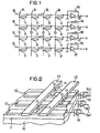
- a memory cell arrangement comprises substantially parallel extending word lines WL and transverse to each other, among themselves substantially parallel bitlines BL (see FIG. 1). Between each one of the bit lines BL and one of the word lines WL is a resistor R connected. A part of the resistors R has a resistance value of 1 mega ohm, the other resistors have a resistance value from 2 mega ohms up. The resistance of 2 Mega-ohm is assigned to the logical value zero, the resistance value of 1 mega ohms, the logical value one. There are 100 bit lines BL and 10,000 word lines WL provided.
- Each of the bit lines BL is connected to the inverting input an operational amplifier OP connected.
- the non-inverting Input of the operational amplifier OP is at ground potential connected.
- the operational amplifier OP is fed back and has a feedback resistor RK.
- one of the word lines WL is selected by applying a signal of, for example, 1 volt. The remaining word lines are grounded. Thereby, a current path is switched between the selected word line WL and each of the bit lines BL. Since the bit lines BL are respectively regulated to 0 volts by the operational amplifiers OP, no current flow takes place between the bit lines BL.
- RK is the resistance of the feedback resistor RK
- R is the resistance of the resistor R
- Rbl is the resistance the bit line BL. This relationship applies because the bit line BL is regulated to 0 volts and the current through the bit line BL via the feedback resistor RK flows.
- a substrate 10 is provided with an insulating layer 11.
- the substrate 10 is, for example, a silicon wafer or the monocrystalline silicon layer of an SOI substrate.
- the insulating layer 11 contains SiO 2 and has a thickness of 100 nm (see FIG. 2).
- bit lines 12 On the surface of the insulating layer 11 are bit lines 12 arranged.
- the bit lines 12 are each strip-shaped and are substantially parallel to each other. They have a length of 10 mm and a width of 0.5 microns on. The distance between adjacent bit lines 12 is 0.5 ⁇ m.
- the bit lines 12 include aluminum or Tungsten. They are made by depositing a whole-area Aluminum layer and subsequent structuring using photolithographic process steps generated. Preferably they become simultaneously in a semiconductor process formed with the production of a metallization level.
- the bit lines 12 are covered with an intermediate oxide layer (not shown). On the surface of the intermediate oxide layer having a thickness of 650 nm and formed of SiO 2 , word lines 13 are arranged. The word lines 13 run transversely to the bit lines 12. The word lines 13 have a length of 100 ⁇ m and a width of 0.5 ⁇ m. The spacing of adjacent word lines 13 is 0.5 .mu.m .
- the word lines are made of aluminum. For this purpose, an aluminum layer is deposited and patterned using photolithographic process steps. Preferably, the word lines 13 are formed simultaneously with the formation of a metallization level in a semiconductor process.
- contact holes 14 are opened after completion of the bit lines 12 and the overlying intermediate oxide layer at those crossing points between one of the word lines 13 and one of the bit lines 12 at which a logic one is stored.
- a photolithographically generated mask is used, which has openings 14 at the locations for the contact holes.
- the contact holes 14 are formed by anisotropic etching, for example with CHF 3 , CF 4 , Ar.
- resistances 15 are formed in the opened contact holes 14. This is done, for example, by forming an Al 2 O 3 layer in a layer thickness of 2 nm, which represents a tunnel oxide layer. Subsequently, the contact hole 14 is filled with aluminum. Alternatively, the resistors 15 are filled with lightly doped polysilicon or lightly doped amorphous silicon having a dopant concentration of 10 14 cm -3 . Another possibility for the formation of the resistors 15 consists in the filling of the contact holes 14 with doped polysilicon having a dopant concentration in the range 10 14 cm -3 and subsequent formation of an SiO 2 layer by thermal oxidation with a layer thickness of 2 nm. The SiO 2 - Layer acts as a tunnel oxide layer. The resistors 15 have a resistance of 1 M ⁇ .
- bit lines 12 are respectively connected to the inverting one Input of an operational amplifier 16 connected. Not inverting input of the operational amplifier 16 is respectively placed at ground potential. The operational amplifier 16 is switched backward coupled.
- the potential becomes the bit lines 12 through the operational amplifier 16, respectively regulated at ground potential.
- the output signal of the operational amplifier 16 thus a Measure the resistance value between a selected one Word line 13 and the associated bit line 12 is effective.
- the resistance between the word lines 13 and the bit lines 12, at their crossing point a zero is stored, infinite. In this case, the output signal almost zero.
- This embodiment therefore has the Advantage that the logical values of zero and one easy to distinguish are.
- an insulating layer 21 is arranged (see FIG. 3).
- the substrate 20 is, for example, a monocrystalline silicon wafer or the monocrystalline silicon layer of an SOI substrate.
- the insulating layer 21 contains SiO 2 and has a thickness of 100 nm.
- strip-shaped auxiliary structures 22 are formed on the surface of the insulating layer 21, strip-shaped auxiliary structures 22 are formed.
- the strip-shaped auxiliary structures 22 are also produced, for example, from SiO 2 by anisotropic etching by means of a photolithographically formed mask.
- the strip-shaped auxiliary structures 22 have a width of 0.5 ⁇ m and a spacing of 0.5 ⁇ m . This width corresponds to the minimum feature width F in a 16 M technology.
- a conductive layer 23 with substantially conformal edge coverage is deposited over the whole area.
- the conductive layer 23 is formed, for example, in a thickness of 150 nm.
- the conductive layer 23 includes, for example, doped polysilicon and metal silicide.
- the doped polysilicon has a dopant concentration of 10 21 cm -3 .
- the metal silicide for example, TiSi 2 or CoSi 2 is suitable.
- conductive spacers 24 are formed on the flanks of the auxiliary structures, which are used as word lines (see Figure 4).
- the conductive spacers 24 are preferably formed simultaneously with other conductive spacers of the same material used in the semiconductor circuit, for example, as gate electrodes or other terminals.
- an intermediate oxide layer 25 is formed, which has a thickness of 400 nm.
- the intermediate oxide layer 25 is formed, for example, from borophosphosilicate glass and has a substantially flat surface.
- the intermediate oxide layer 25 covers the auxiliary structures 22 and the conductive spacer 24.
- contact holes 27 open at those crossing points between one of the bit lines 26 and one of the conductive spacers 24, which serve as word lines at which a logical one is stored.
- contact holes 27 open at those crossing points between one of the bit lines 26 and one of the conductive spacers 24, which serve as word lines at which a logical one is stored.
- two conductive spacers 24 come and the contact holes 27 with dimensions can be formed from minimal F fall adjacent Contact holes 27 together. This is in FIG. 4 indicated by the dotted line.
- resistors 28 the contact holes 27 then filled up.
- the same materials are used, which in the basis of Figure 2 described embodiment have been explained.
- bit lines 26 On the surface of the intermediate oxide layer 25 and the padded Contact holes 27 becomes a conductive layer for Example of aluminum deposited and using photolithographic Process steps structured to bit lines 26 to build.
- the bit lines 26 are transverse to the conductive ones Spacers 24.
- the bit lines 26 are parallel to second level.
- bit lines 26 are, as explained with reference to FIGS. 1 and 2, each with the inverting input of an operational amplifier connected. The further interconnection of the operational amplifier and the readout procedure is analogous as explained with reference to FIGS. 1 and 2.
Landscapes
- Semiconductor Memories (AREA)
- Read Only Memory (AREA)
Description
- Figur 1
- zeigt eine Architektur für eine Speicherzellenanordnung, in der die logischen Werte Null und Eins durch unterschiedliche Widerstände realisiert sind.
- Figur 2
- zeigt einen Ausschnitt aus einer Speicherzellenanordnung, in der die logischen Werte Null und Eins durch Bildung keines Kontaktloches oder eines Kontaktloches mit einem Widerstand realisiert sind.
- Figur 3
- und 4 zeigt Herstellschritte zur Bildung einer Speicherzellenanordnung, die als Wortleitungen leitfähige Spacer aufweist.
Claims (4)
- Speicherzellenanordnung,umfassen.bei der in einem Halbleiterschichtaufbau (10,11) parallel verlaufende Wortleitungen (13) und parallel verlaufende Bitleitungen (12) vorhanden sind, wobei die Wortleitungen (13) und die Bitleitungen (12) quer zueinander verlaufen und zwischen den Wortleitungen (13) und den Bitleitungen (12) eine isolierende Schicht angeordnet ist,bei der zwischen Wortleitungen (13) und Bitleitungen (12) Widerstände (15) geschaltet sind, die hochohmiger als die Wortleitungen (13) und die Bitleitungen (12) sind und die jeweils in einem Kontaktloch (14) angeordnet sind, das in der isolierenden Schicht an einem Kreuzungspunkt zwischen einer der Bitleitungen (12) und einer der Wortleitungen (13) zwischen der jeweiligen Bitleitung (12) und der jeweiligen Wortleitung (13) angeordnet ist,bei der die Bitleitungen (12) jeweils mit einem Leseverstärker (16) verbunden sind, über den das Potential an der jeweiligen Bitleitung (12) auf ein Referenzpotential regelbar ist und an dem ein Ausgangssignal abgreifbar ist und welcher einen rückgekoppelten Operationsverstärker (16) aufweist,bei der die Widerstände (15) erste Widerstände oder zweite Widerstände mit unterschiedlichen Widerstandswerten umfassen, wobei die ersten Widerstände einen ersten logischen Wert und die zweiten Widerstände einen zweiten logischen Wert repräsentieren,bei der die ersten oder zweiten Widerständei) eine erste isolierende Tunnelschicht, insbesondere Al2O3 oder SiO2, undii) eine sich daran anschließende leitfähige Schicht, insbesondere dotiertes amorphes oder polykristallines Silizium,
- Speicherzellenanordnung nach Anspruch 1, bei der die Anzahl der Wortleitunge (13) größer als die Anzahl der Bitleitungen (12) ist.
- Verfahren zur Herstellung einer Speicherzellenanordnung,in den Kontaktlöchern (14) hergestellt werden.bei dem auf der Oberfläche eines Substrats (10) parallel verlaufende Wortleitungen (13) und eine parallel verlaufende Bitleitungen (12) und eine isolierende Schicht gebildet werden, wobei die Wortleitungen (13) quer zu den Bitleitungen (12) verlaufen und wobei die isolierende Schicht zwischen den Wortleitungen (13) und den Bitleitungen (12) angeordnet ist,bei dem an vorgegebenen Kreuzungspunkten zwischen Bitleitungen (12) und Wortleitungen (13) in der isolierenden Schicht Kontaktlöcher (14) geöffnet werden, die jeweils zwischen einer der Bitleitungen (12) und einer der Wortleitungen (13) angeordnet sind, in denen jeweils ein Widerstand (15) realisiert wird, der zwischen die jeweilige Bitleitung (12) und die jeweilige Wortleitung (13) geschaltet ist und der hochohmiger als die Bitleitunge (12) und die Wortleitungen (13) ist,bei dem Leseverstärker (16) erzeugt werden, die mit jeweils einer der Bitleitungen (12) verbunden werden, über die das Potential an der jeweiligen Bitleitung (12) auf ein Referenzpotential regelbar ist und an dem ein Ausgangssignal abgreifbar ist.bei dem die Widerstände (15) durch Bildungi) einer ersten isolierenden Tunnelschicht, insbesondere Al2O3 oder SiO2, undii) einer sich daran anschließenden leitfähigen Schicht, insbesondere dotiertes amorphes oder polykristallines Silizium,
- Verfahren nach Anspruch 3,bei dem zur Bildung der Wortleitungen (13) unächst eine Hilfsstruktur (22) erzeugt wird, die streifenförmige Elemente auf-weist,bei dem eine leitfähige Schicht (23) mit konformer Kantenbedeckung erzeugt wird,bei dem durch anisotropes, zur Hilfsstruktur (22) selektives Ätzen die Wortleitungen (13) in Form von leitfähigen Spacern (24) aus der leitfähigen Schicht (23) gebildet werden.
Applications Claiming Priority (3)
| Application Number | Priority Date | Filing Date | Title |
|---|---|---|---|
| DE19740945 | 1997-09-17 | ||
| DE19740945 | 1997-09-17 | ||
| PCT/DE1998/002618 WO1999014808A1 (de) | 1997-09-17 | 1998-09-04 | Speicherzellenanordnung und verfahren zu deren herstellung |
Publications (2)
| Publication Number | Publication Date |
|---|---|
| EP1008183A1 EP1008183A1 (de) | 2000-06-14 |
| EP1008183B1 true EP1008183B1 (de) | 2005-11-30 |
Family
ID=7842685
Family Applications (1)
| Application Number | Title | Priority Date | Filing Date |
|---|---|---|---|
| EP98954117A Expired - Lifetime EP1008183B1 (de) | 1997-09-17 | 1998-09-04 | Speicherzellenanordnung und verfahren zu deren herstellung |
Country Status (5)
| Country | Link |
|---|---|
| US (1) | US6417043B1 (de) |
| EP (1) | EP1008183B1 (de) |
| DE (1) | DE59813243D1 (de) |
| TW (1) | TW416057B (de) |
| WO (1) | WO1999014808A1 (de) |
Families Citing this family (3)
| Publication number | Priority date | Publication date | Assignee | Title |
|---|---|---|---|---|
| US7177181B1 (en) * | 2001-03-21 | 2007-02-13 | Sandisk 3D Llc | Current sensing method and apparatus particularly useful for a memory array of cells having diode-like characteristics |
| US6625055B1 (en) * | 2002-04-09 | 2003-09-23 | Hewlett-Packard Development Company, L.P. | Multiple logical bits per memory cell in a memory device |
| DE10349009B4 (de) * | 2002-10-18 | 2008-02-14 | Fresenius Medical Care Deutschland Gmbh | Anordnung zum Speichern von Daten und Verfahren und Vorrichtung zum Lesen der Daten |
Family Cites Families (19)
| Publication number | Priority date | Publication date | Assignee | Title |
|---|---|---|---|---|
| FR2071501A5 (de) * | 1969-12-31 | 1971-09-17 | Dondoux Jacques | |
| US3863231A (en) * | 1973-07-23 | 1975-01-28 | Nat Res Dev | Read only memory with annular fuse links |
| US4831427A (en) * | 1987-07-23 | 1989-05-16 | Texas Instruments Incorporated | Ferromagnetic gate memory |
| US5429988A (en) * | 1994-06-13 | 1995-07-04 | United Microelectronics Corporation | Process for producing high density conductive lines |
| US6194751B1 (en) * | 1994-11-15 | 2001-02-27 | Radiant Technologies, Inc | Ferroelectric based memory devices utilizing low Curie point ferroelectrics and encapsulation |
| US5607599A (en) * | 1994-11-17 | 1997-03-04 | Kabushiki Kaisha Toshiba | Method of processing a magnetic thin film |
| JPH08255843A (ja) * | 1995-03-15 | 1996-10-01 | Sony Corp | 半導体rom装置及びそのデータ書き込み方法 |
| US5640343A (en) | 1996-03-18 | 1997-06-17 | International Business Machines Corporation | Magnetic memory array using magnetic tunnel junction devices in the memory cells |
| US5920500A (en) * | 1996-08-23 | 1999-07-06 | Motorola, Inc. | Magnetic random access memory having stacked memory cells and fabrication method therefor |
| TW348360B (en) * | 1996-08-23 | 1998-12-21 | Samsung Electronics Co Ltd | Display device |
| US5847442A (en) * | 1996-11-12 | 1998-12-08 | Lucent Technologies Inc. | Structure for read-only-memory |
| TW307048B (en) * | 1996-11-22 | 1997-06-01 | United Microelectronics Corp | High density read only memory structure and manufacturing method thereof |
| US5863231A (en) | 1997-05-19 | 1999-01-26 | Strong; Jeffrey W. | Underwater exhaust system for marine engine |
| JP3061117B2 (ja) * | 1997-06-18 | 2000-07-10 | 日本電気株式会社 | 半導体装置の製造方法 |
| US6130835A (en) * | 1997-12-02 | 2000-10-10 | International Business Machines Corporation | Voltage biasing for magnetic RAM with magnetic tunnel memory cells |
| US6104633A (en) * | 1998-02-10 | 2000-08-15 | International Business Machines Corporation | Intentional asymmetry imposed during fabrication and/or access of magnetic tunnel junction devices |
| US6130814A (en) * | 1998-07-28 | 2000-10-10 | International Business Machines Corporation | Current-induced magnetic switching device and memory including the same |
| US6163477A (en) * | 1999-08-06 | 2000-12-19 | Hewlett Packard Company | MRAM device using magnetic field bias to improve reproducibility of memory cell switching |
| JP3484380B2 (ja) * | 1999-09-22 | 2004-01-06 | 沖電気工業株式会社 | リードオンリメモリ |
-
1998
- 1998-08-26 TW TW087114062A patent/TW416057B/zh not_active IP Right Cessation
- 1998-09-04 EP EP98954117A patent/EP1008183B1/de not_active Expired - Lifetime
- 1998-09-04 DE DE59813243T patent/DE59813243D1/de not_active Expired - Fee Related
- 1998-09-04 WO PCT/DE1998/002618 patent/WO1999014808A1/de not_active Ceased
-
2000
- 2000-03-17 US US09/528,268 patent/US6417043B1/en not_active Expired - Lifetime
Also Published As
| Publication number | Publication date |
|---|---|
| DE59813243D1 (de) | 2006-01-05 |
| US6417043B1 (en) | 2002-07-09 |
| TW416057B (en) | 2000-12-21 |
| EP1008183A1 (de) | 2000-06-14 |
| WO1999014808A1 (de) | 1999-03-25 |
Similar Documents
| Publication | Publication Date | Title |
|---|---|---|
| DE4434725C1 (de) | Festwert-Speicherzellenanordnung und Verfahren zu deren Herstellung | |
| EP0783180B1 (de) | Elektrisch programmierbare Speicherzellenanordnung und Verfahren zu deren Herstellung | |
| DE69803782T2 (de) | Festwertspeicher und festwertspeicheranordnungen | |
| DE69824293T2 (de) | Ferroelektrische datenverarbeitungsanordnung | |
| DE60308568T2 (de) | Magnetisches Joch in MRAM zur Reduzierung des Programmierungsleistungsverbrauchs und Herstellungsverfahren | |
| DE69226405T2 (de) | Geschichtete CMOS SRAM Zelle mit polysilizium-Lasttransistoren | |
| DE602004010859T2 (de) | Verfahren zur Herstellung einer Widerstands-Kreuzpunkt-Speicheranordnung im Nanometerbereich und Vorrichtung | |
| DE602004005333T2 (de) | Planarer polymer-speicherbaustein | |
| DE3513034C2 (de) | Verfahren zur Herstellung einer Halbleitervorrichtung | |
| DE2654728B2 (de) | Programmierbarer Festwertspeicher und Verfahren zu seiner Herstellung | |
| WO1998053504A1 (de) | Ein-elektron-speicherbauelement | |
| EP0783181A1 (de) | Elektrisch programmierbare Speicherzellenanordnung und Verfahren zu deren Herstellung | |
| DE3844120A1 (de) | Halbleitereinrichtung mit grabenfoermiger struktur | |
| DE60304209T2 (de) | Magnettunnelsperrschichtspeicherzellenarchitektur | |
| DE3224287C2 (de) | ||
| EP0946985B1 (de) | Speicherzellenanordnung und verfahren zu deren herstellung | |
| EP1145319B1 (de) | Integrierte schaltungsanordnung und verfahren zu deren herstellung | |
| DE19824209A1 (de) | Halbleitervorrichtung | |
| DE19748495C2 (de) | EEPROM-Zellstruktur und Verfahren zum Programmieren bzw. Löschen ausgewählter EEPROM-Zellstrukturen sowie EEPROM-Zellenfeld | |
| EP0815594B1 (de) | Festwert-speicherzellenanordnung und verfahren zu deren herstellung | |
| DE3930639A1 (de) | Halbleiterspeichervorrichtung | |
| EP0045403B1 (de) | Verefahren zur Herstellung einer Anordnung zum Verringern der Strahlungsempfindlichkeit von in integrierter MOS-Schaltkreistechnik ausgeführten Speicherzellen | |
| DE3153137C2 (de) | ||
| DE4327653C2 (de) | Nichtflüchtige Halbleiterspeichervorrichtung mit verbessertem Koppelverhältnis und Verfahren zur Herstellung einer solchen | |
| DE10082909B4 (de) | Nichtflüchtige ferroelektrische Speicherzelle, nichtflüchtiger ferroelektrischer Speicher und Verfahren zu seiner Herstellung |
Legal Events
| Date | Code | Title | Description |
|---|---|---|---|
| PUAI | Public reference made under article 153(3) epc to a published international application that has entered the european phase |
Free format text: ORIGINAL CODE: 0009012 |
|
| AK | Designated contracting states |
Kind code of ref document: A1 Designated state(s): DE |
|
| 17P | Request for examination filed |
Effective date: 20000317 |
|
| 17Q | First examination report despatched |
Effective date: 20011128 |
|
| GRAP | Despatch of communication of intention to grant a patent |
Free format text: ORIGINAL CODE: EPIDOSNIGR1 |
|
| GRAS | Grant fee paid |
Free format text: ORIGINAL CODE: EPIDOSNIGR3 |
|
| GRAA | (expected) grant |
Free format text: ORIGINAL CODE: 0009210 |
|
| AK | Designated contracting states |
Kind code of ref document: B1 Designated state(s): DE |
|
| REF | Corresponds to: |
Ref document number: 59813243 Country of ref document: DE Date of ref document: 20060105 Kind code of ref document: P |
|
| PLBE | No opposition filed within time limit |
Free format text: ORIGINAL CODE: 0009261 |
|
| STAA | Information on the status of an ep patent application or granted ep patent |
Free format text: STATUS: NO OPPOSITION FILED WITHIN TIME LIMIT |
|
| 26N | No opposition filed |
Effective date: 20060831 |
|
| PGFP | Annual fee paid to national office [announced via postgrant information from national office to epo] |
Ref country code: DE Payment date: 20071113 Year of fee payment: 10 |
|
| PG25 | Lapsed in a contracting state [announced via postgrant information from national office to epo] |
Ref country code: DE Free format text: LAPSE BECAUSE OF NON-PAYMENT OF DUE FEES Effective date: 20090401 |