EP1007262B1 - Soldering iron tip and method of making the same - Google Patents
Soldering iron tip and method of making the same Download PDFInfo
- Publication number
- EP1007262B1 EP1007262B1 EP98905032A EP98905032A EP1007262B1 EP 1007262 B1 EP1007262 B1 EP 1007262B1 EP 98905032 A EP98905032 A EP 98905032A EP 98905032 A EP98905032 A EP 98905032A EP 1007262 B1 EP1007262 B1 EP 1007262B1
- Authority
- EP
- European Patent Office
- Prior art keywords
- tip
- soldering iron
- cap
- soldering
- core member
- Prior art date
- Legal status (The legal status is an assumption and is not a legal conclusion. Google has not performed a legal analysis and makes no representation as to the accuracy of the status listed.)
- Expired - Lifetime
Links
- XEEYBQQBJWHFJM-UHFFFAOYSA-N Iron Chemical compound [Fe] XEEYBQQBJWHFJM-UHFFFAOYSA-N 0.000 title claims abstract description 155
- 229910052742 iron Inorganic materials 0.000 title claims abstract description 79
- 238000005476 soldering Methods 0.000 title claims abstract description 73
- 238000004519 manufacturing process Methods 0.000 title description 9
- PXHVJJICTQNCMI-UHFFFAOYSA-N nickel Substances [Ni] PXHVJJICTQNCMI-UHFFFAOYSA-N 0.000 claims abstract description 28
- 229910052751 metal Inorganic materials 0.000 claims abstract description 21
- 239000002184 metal Substances 0.000 claims abstract description 21
- 229910052759 nickel Inorganic materials 0.000 claims abstract description 16
- 239000011651 chromium Substances 0.000 claims abstract description 13
- 229910052804 chromium Inorganic materials 0.000 claims abstract description 12
- 229910001220 stainless steel Inorganic materials 0.000 claims abstract description 7
- 239000010935 stainless steel Substances 0.000 claims abstract description 5
- 238000005260 corrosion Methods 0.000 claims abstract 2
- 230000007797 corrosion Effects 0.000 claims abstract 2
- 239000011162 core material Substances 0.000 claims description 20
- 229910000679 solder Inorganic materials 0.000 claims description 12
- VYZAMTAEIAYCRO-UHFFFAOYSA-N Chromium Chemical compound [Cr] VYZAMTAEIAYCRO-UHFFFAOYSA-N 0.000 claims description 10
- 229910001030 Iron–nickel alloy Inorganic materials 0.000 claims description 6
- 229910000599 Cr alloy Inorganic materials 0.000 claims 1
- 229910000640 Fe alloy Inorganic materials 0.000 claims 1
- 229910000990 Ni alloy Inorganic materials 0.000 claims 1
- 239000000788 chromium alloy Substances 0.000 claims 1
- 238000004090 dissolution Methods 0.000 claims 1
- 239000010410 layer Substances 0.000 abstract description 60
- 238000000034 method Methods 0.000 abstract description 58
- 239000000463 material Substances 0.000 abstract description 39
- RYGMFSIKBFXOCR-UHFFFAOYSA-N Copper Chemical compound [Cu] RYGMFSIKBFXOCR-UHFFFAOYSA-N 0.000 abstract description 32
- 239000010949 copper Substances 0.000 abstract description 25
- 229910052802 copper Inorganic materials 0.000 abstract description 24
- 238000005219 brazing Methods 0.000 abstract description 17
- 229910045601 alloy Inorganic materials 0.000 abstract description 16
- 239000000956 alloy Substances 0.000 abstract description 16
- 239000011241 protective layer Substances 0.000 abstract description 12
- 230000001681 protective effect Effects 0.000 abstract description 11
- 238000005520 cutting process Methods 0.000 abstract description 3
- 238000009713 electroplating Methods 0.000 description 18
- 229910000881 Cu alloy Inorganic materials 0.000 description 6
- 239000011248 coating agent Substances 0.000 description 6
- 238000000576 coating method Methods 0.000 description 6
- 235000000396 iron Nutrition 0.000 description 6
- 230000015572 biosynthetic process Effects 0.000 description 5
- 229910018487 Ni—Cr Inorganic materials 0.000 description 4
- 238000002788 crimping Methods 0.000 description 4
- 238000003754 machining Methods 0.000 description 4
- 239000003792 electrolyte Substances 0.000 description 3
- 238000007493 shaping process Methods 0.000 description 3
- 229910052709 silver Inorganic materials 0.000 description 3
- 230000009466 transformation Effects 0.000 description 3
- 239000002131 composite material Substances 0.000 description 2
- 238000000151 deposition Methods 0.000 description 2
- 230000008018 melting Effects 0.000 description 2
- 238000002844 melting Methods 0.000 description 2
- 239000000203 mixture Substances 0.000 description 2
- 239000004332 silver Substances 0.000 description 2
- 238000005245 sintering Methods 0.000 description 2
- 229910052714 tellurium Inorganic materials 0.000 description 2
- 230000001131 transforming effect Effects 0.000 description 2
- KJTLSVCANCCWHF-UHFFFAOYSA-N Ruthenium Chemical compound [Ru] KJTLSVCANCCWHF-UHFFFAOYSA-N 0.000 description 1
- 239000002253 acid Substances 0.000 description 1
- 238000010420 art technique Methods 0.000 description 1
- 230000000593 degrading effect Effects 0.000 description 1
- 238000007772 electroless plating Methods 0.000 description 1
- 230000005496 eutectics Effects 0.000 description 1
- 238000011031 large-scale manufacturing process Methods 0.000 description 1
- 229910021645 metal ion Inorganic materials 0.000 description 1
- 239000007769 metal material Substances 0.000 description 1
- 229910052762 osmium Inorganic materials 0.000 description 1
- SYQBFIAQOQZEGI-UHFFFAOYSA-N osmium atom Chemical compound [Os] SYQBFIAQOQZEGI-UHFFFAOYSA-N 0.000 description 1
- 230000003647 oxidation Effects 0.000 description 1
- 238000007254 oxidation reaction Methods 0.000 description 1
- 239000006072 paste Substances 0.000 description 1
- 238000007747 plating Methods 0.000 description 1
- 239000000843 powder Substances 0.000 description 1
- 229910052707 ruthenium Inorganic materials 0.000 description 1
- 239000007787 solid Substances 0.000 description 1
- 239000007858 starting material Substances 0.000 description 1
- 239000000126 substance Substances 0.000 description 1
- PORWMNRCUJJQNO-UHFFFAOYSA-N tellurium atom Chemical compound [Te] PORWMNRCUJJQNO-UHFFFAOYSA-N 0.000 description 1
Images


Classifications
-
- B—PERFORMING OPERATIONS; TRANSPORTING
- B23—MACHINE TOOLS; METAL-WORKING NOT OTHERWISE PROVIDED FOR
- B23K—SOLDERING OR UNSOLDERING; WELDING; CLADDING OR PLATING BY SOLDERING OR WELDING; CUTTING BY APPLYING HEAT LOCALLY, e.g. FLAME CUTTING; WORKING BY LASER BEAM
- B23K3/00—Tools, devices, or special appurtenances for soldering, e.g. brazing, or unsoldering, not specially adapted for particular methods
- B23K3/02—Soldering irons; Bits
- B23K3/03—Soldering irons; Bits electrically heated
- B23K3/0338—Constructional features of electric soldering irons
-
- B—PERFORMING OPERATIONS; TRANSPORTING
- B23—MACHINE TOOLS; METAL-WORKING NOT OTHERWISE PROVIDED FOR
- B23K—SOLDERING OR UNSOLDERING; WELDING; CLADDING OR PLATING BY SOLDERING OR WELDING; CUTTING BY APPLYING HEAT LOCALLY, e.g. FLAME CUTTING; WORKING BY LASER BEAM
- B23K3/00—Tools, devices, or special appurtenances for soldering, e.g. brazing, or unsoldering, not specially adapted for particular methods
- B23K3/02—Soldering irons; Bits
- B23K3/025—Bits or tips
- B23K3/026—Removable soldering bits
-
- B—PERFORMING OPERATIONS; TRANSPORTING
- B32—LAYERED PRODUCTS
- B32B—LAYERED PRODUCTS, i.e. PRODUCTS BUILT-UP OF STRATA OF FLAT OR NON-FLAT, e.g. CELLULAR OR HONEYCOMB, FORM
- B32B15/00—Layered products comprising a layer of metal
- B32B15/01—Layered products comprising a layer of metal all layers being exclusively metallic
- B32B15/013—Layered products comprising a layer of metal all layers being exclusively metallic one layer being formed of an iron alloy or steel, another layer being formed of a metal other than iron or aluminium
- B32B15/015—Layered products comprising a layer of metal all layers being exclusively metallic one layer being formed of an iron alloy or steel, another layer being formed of a metal other than iron or aluminium the said other metal being copper or nickel or an alloy thereof
Definitions
- the present invention relates to soldering iron tips having protective outer layers.
- FIG. 1 illustrates an exemplary tip 1 formed by machining a monolithic rod of copper or a copper alloy 2 .
- copper tips also have a number of undesirable properties. When heated to the high temperatures required for soldering, the tips may dissolve in the solder and/or corrode in air. Furthermore, the tips may deform when mechanical pressure is applied thereto. For this reason, simple copper-based soldering tips have a relatively low tip life.
- the prior art has addressed this problem by coating the copper tips with one or more outer layers. More specifically, as illustrated in Figure 2, the end of the tapered portion of the tip 1 (referred to as the "working area") is coated with an outer layer 4 of iron (Fe).
- the iron coating 4 protects the softer copper core 2 from deformation during soldering operations, and from dissolving in the solder. Iron is also readily wettable by molten solder.
- the remainder of the soldering iron tip 1 is covered by other types of materials 6 , such as a layer of chromium (Cr) or a layer of chromium formed over a layer of nickel (Ni).
- These layers 6 provide a good electrical connection between the tip of the soldering iron and ground, thus ensuring a low tip-to-ground voltage potential and resistance. These layers 6 also protect the copper 2 from corroding in air. Furthermore, chromium offers poor wettability by the solder and thereby prevents the solder from creeping up the tip from the working area and degrading the performance of the soldering iron tip.
- Electroplating involves applying a voltage between the soldering iron tip (cathode), and pieces of the metal to be deposited (the anode), through an acid-based aqueous electrolyte.
- the soldering iron tip and the metal anode are both submersed in the electrolyte.
- the applied voltage causes metal ions to flow from the anode to the cathode (soldering iron tip) through the electrolyte, thus depositing the metal onto the tip of the soldering iron in a controlled fashion.
- 3,315,350 proposes a technique for electroplating a layer of iron on a copper tip, and then electroplating an additional layer of nickel and chromium on the iron layer.
- U.S. Patent No. 3,986,653 proposes electroplating an outer layer of osmium or ruthenium (or an alloy thereof) on a soldering iron tip.
- Electroplating of copper soldering iron tips has disadvantages.
- electroplating sometimes produces a coating of uneven thickness on the tip, especially at regions where the contour of the tip abruptly changes.
- the process itself is inherently unstable, resulting in differences in plating thickness and quality from one production batch to the next.
- electroplating is relatively expensive, which is partially due to the large amount of manual labor required by the technique, and the need to dispose of the chemical solutions used in the process in an environmentally safe manner.
- U.S. Patent No. 4,055,744 discloses a technique for forming a hardened outer layer on the working area of a soldering tip by separately forming an iron cap, and then mechanically crimping the cap onto the soldering iron tip.
- the composite structure of the cap and the tip is further shaped by manually hammering the composite structure, or by using a swaging machine. While avoiding the problems associated with electroplating, crimping the cap to the copper tip may tightly bind the cap to the tip only at selective locations of the tip, such as at the base of the tip, thereby reducing the contact area between the tip and the cap. This, in turn, may reduce the transfer of heat from the tip to the cap, thus reducing the performance or the efficiency of the soldering iron.
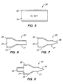
- a heater 8 is the component of the soldering iron which actually generates heat. That is, the electrical coils of the soldering iron (not shown) transfer energy to the heater 8 , which in turn transfers heat to the working area of the soldering iron tip 1 .
- the heater 8 element comprises a clad wire segment having an inner core 12 and an outer layer 10 formed thereon. The heater element 8 is press fit into a machined hole 14 located in the back of the tip 1 .
- the mechanical interface 16 (in Figure 4) between the heater 8 and the tip 1 impedes the transfer of heat from the heater 8 to the tip 1 .
- soldering iron tip is produced by cutting a lengh of clad wire into a plurality of segments, where each segment comprises a core of material (such as copper) and an outer protective layer (such as stainless steel, nickel of high purity, chromium of high purity, Fe-Ni alloys such as Invar-type alloys, or other suitable material). Each clad wire segment is then shaped into a soldering iron tip by a cold heading process, or other metal forming process.
- the outer protective layer is disposed "behind" the working area of the tip, and provides good electrical conductivity between the tip and ground, thus maintaining a low tip-to-ground voltage potential and resistance.
- the outer layer also protects the inner core (of copper) from oxidation, and offers poor wettability, which prevents solder from adhering thereto.
- the clad wire segment can be further shaped to form an integrated heater element located on one end of the tip. Since the heater element is formed from the same segment of the clad wire segment as the tip itself, this technique ensures metallurgical continuity between the heater and the working area of the tip, and thereby improves the transfer of heat between the heater and the tip by eliminating the mechanical interface 16 shown in Figure 4.
- the above described metal forming steps can be performed on a wire (or rod) segment which does not include a protective outer layer.
- a protective outer layer for the working area of the soldering iron tip is formed by inserting a separately formed cap of iron (or like material) over the working area portion of the tip. More specifically, the technique entails producing a thin strip or sheet of protective layer material, such as iron. Tapered caps are then stamped out of the sheet using a die having a shape which resembles the shape of the soldering iron tip. The caps formed in this manner are then inserted over the working area of the soldering iron tips, and attached thereto by applying brazing material to the caps or the tips and then melting or sintering the brazing material. Alternatively, the brazing material can be applied directly to the strip of material (before stamping is performed) to further expedite the manufacturing process. In either event, the use of brazing, or like technique, improves the thermal conductivity between the tip and the cap by creating an intimate metallurgical bond between the tip and the cap, as compared with the prior art technique of crimping the cap to the tip.
- a clad wire or rod segment is used to form a soldering tip including one or more protective outer layers on the working area of the soldering tip.
- soldering irons heat and remove previously applied solder.
- a clad wire (or rod) segment 20 comprises a core of material 24 , on which another electrically conductive protective layer 22 is metallurgically bonded.
- the core material 24 may comprise a metal such as copper of high purity, such as copper alloy Nos. C10100 or C10200 having copper contents of 99.99% Cu and 99.95% Cu, respectively.
- copper alloy containing tellurium can be used, such as copper alloy No. C14500 (comprised of 99.5% Cu, 0.5% Te and 0.008% P).
- the protective layer 22 can comprise, but is not limited to, high purity nickel, high purity chromium, or some alloy thereof, such as Fe-Ni (e.g. Invar-type alloys), Fe-Ni-Cr, or other suitable material.
- the layer 22 can also comprise stainless steel.
- clad wire produced by Anomet Products, Inc. of Shrewsbury, Mass. can be used to produce soldering iron tips according to techniques disclosed herein.
- a semi-finished tip produced by the clad wire segment 20 is shown in Figure 6 (in cross-section depiction), while a finished tip produced by the clad wire segment 20 is shown in Figure 7 (in cross-section depiction) .
- the tip has a cylindrical portion 23 joined to a cylindrical portion 21 . of smaller diameter.
- the portion 21 terminates in a tapered working area 28 .
- the outer layer 22 of the clad wire covers the underlying copper core 24 , except for the working area 28 of the tip.
- the protective outer layer 22 serves a number of purposes.
- the layer 22 protects the underlying copper core 24 from corroding in the air.
- the outer layer 22 provides a good electrical contact between the tip and ground, which, in turn, prevents a voltage from building up between the tip and ground which could discharge during soldering operations and damage the components to which solder is being applied.
- soldering electrical components military specifications require a tip-to-ground voltage potential of no more than 2 millivolts (mv) and tip-to-ground resistance of no more than 2 ohms.
- the outer layer 22 offers relatively poor wettability by solder, and thereby prevents solder from advancing past the working area of the soldering iron tip.
- the use of the clad wire or rod as a starting material eliminates the need to form the protective outer layer 22 by electroplating at a later stage in the production of the tip, and therefore eliminates the above-described drawbacks of electroplating.
- the finished tip (or semi-finished tip) with an integral heater includes a cylindrical portion 23 sandwiched between the cylindrical portion 21 and a heater element 26 (as shown in cross-section depiction).
- the beater element 26 and the tip itself are formed from the same clad wire (or rod) segment 20 .
- the outer layer 22 from the clad wire covers the tip, including the heater 26 , but does not cover the tapered end portion 28 of the tip.
- the protective layer 22 can comprise, but is not limited to, stainless steel, high purity nickel, high purity chromium, or some alloy thereof, such as Fe-Ni (e.g. Invar-type alloys), Fe-Ni-Cr, or other suitable material. More specifically, Invar-type alloys of different compositions can be selected to provide different soldering iron power load capacities. For example, progressively greater power loads can be supplied by layers of: (1) 42% Ni, 6% Cr, 52% Fe; (2) 42% Ni, 58% Fe; (3) 44% Ni, 56% Fe; and (4) 52% Ni, 48% Fe.
- clad wire (or rod) segment 20 shown in Figure 5 into a desired tip geometry (such as the tip shapes shown in Figures 6, 7 or 8), including machining the wire or rod segment 20 into the desired shape.
- a metal forming process such as cold or hot heading can be used to manufacture the tip.
- Figure 9 illustrates one exemplary technique employing a cold heading process for transforming a wire segment into a finished or semi-finished tip.
- the exemplary technique begins by feeding a length of clad wire from a spool of wire to a cutter (step S1 ), which cuts off a segment of the wire of prescribed length (step S2 ). Following the cutting operation, the segment is then transported to a first die chamber (step S3 ), where one or more dies deliver one or more blows to taper one end of the segment (step S4 ) to shape a portion 21 having a reduced diameter, as shown in Figure 6, which is then further processed to shape a tapered working area 28 , as shown in Figure 7.
- the process can skip steps S5 and S6 , upon which the part is dispensed in step S7 .
- the protective layer 22 can be removed from the working area 28 of the tip by machining or like technique.
- a protective layer can be added to the working area 28 at some later stage of production using any suitable technique, such as by using electroplating, or by fitting a cap onto the working area 28 (to be discussed later).
- the tip shown in Figure 7 can be transported to a second die chamber (step S5 ), where another die delivers one or more blows to form the heater element 26 at one end of the tip (step S6 ), as shown in Figure 8, thus producing the finished tip with an integrated heater 26 .
- the finished tip is dispensed in step S7 .
- Steps S5 and S6 are enclosed in a broken-line box to illustrate that they can be omitted to produce a tip without an integrated heater, if desired.
- Alternative methods for constructing the tip include using a hot heading process (instead of a cold heading process), or forming the heater 26 prior to forming the portions 21 , 28 , or forming the heater 26 at the same time as the portions 21 , 28 (e.g. through the simultaneous application of plural blows from plural dies).
- the exemplary steps shown in Figure 9 can be fully automated, or may require manipulation of parts and/or machinery by a human operator.
- the tip portions e.g. portions 21 , 23
- the process discussed above shapes the clad wire segment 20 shown in Figure 5.
- the technique can also be used to shape wire segments which do not have an outer protective layer 22 .
- the protective layer 22 could be subsequently formed on the shaped tips through electroplating or like technique.
- Figures 10-12 illustrate another feature of the present invention for forming a hardened outer layer on the working area of the tip.
- the technique shown in Figures 10 through 12 has wide applicability to many types of tips produced by various techniques.
- the technique shown in Figures 10 through 12 can be used to supply a hardened outer layer on the exposed end 28 of the soldering iron tip produced by the method described with reference to Figures 5 through 9, or can be used to supply a hardened outer layer for machined copper cores, such as the machined core 2 shown in Figure 1.
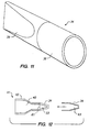
- a continuous thin strip of material 30 is produced (e.g. a strip having a thickness of about 5 mils (127 ⁇ m).
- the material can comprise iron of high purity (e.g. iron having a purity of 99.5% in one exemplary embodiment), nickel, or other material or alloy.
- a plurality of caps 34 are stamped out using die 32 which mates with die 35 . Only one pair of dies ( 32 , 35 ) has been shown to facilitate discussion, although plural pairs of dies ( 32 , 35 ) can be used.
- the die 32 has an outer contour 37 which defines the inner contour of the cap 34
- the die 35 has a recess having a contour 39 which defines the outer geometrical shape of the cap 34 .
- Figure 11 shows one such exemplary shaped cap 34 , having a tapered end 38 and a cylindrical portion 36 .
- the cap 34 can alternatively be formed by other techniques such as, but not limited to, a deep drawing process.
- the cap 34 is then inserted over the working area 33 of a tip 41 in the manner shown in Figure 12.
- the cap 34 is preferably secured to the tip 41 by a metallurgical bonding technique such as brazing, or like technique.
- a metallurgical bonding technique such as brazing, or like technique.
- a small amount e.g. about 0.2 mils (5 ⁇ m)
- CUSIL high purity silver
- the brazing material can be applied to the strip of material 30 before stamping. During melting, the silver and copper form a CuAg eutectic which bonds the cap to the tip.
- the cap 34 may be produced by cold heading or forming segments of wire or metal shapes (e.g. spheres) into the desired tapered shape.
- segments of wire or metal shapes e.g. spheres
- U.S. Patent No. 3,669,334 discloses one such technique.
- the finished soldering iron tip 41 shown in cross-section depiction in Figure 12 comprises a copper core 40 having a tapered working area end 33 .
- the cap 34 is inserted over the working area end 33 .
- the cap 34 can contact another layer 42 (or series of layers).
- These additional layers 42 can be formed by any suitable technique. For instance, these layers 42 can be formed by the technique shown in Figures 5-9, or via electroplating. Alternatively, these layers 42 can themselves be separately formed as caps and inserted over the core 40 prior to inserting the cap 34 , such that the tip has a plurality of overlapping caps. In any event, these layers 42 preferably have low wettability by solder and provide low tip-to-ground potential, as previously described.
- this technique can be used to furnish caps 34 for tips which include integrated heaters (such as the tip shown in Figure 8).
- the outer contour of the working area 33 generally matches the inner contour of the cap 34 .
- the terminal end of the tip need not match the inner contour of the cap 34 .
- the terminal end of the tip can be truncated along the line 61 , thereby forming an intermediary region between the end of the tip and the cap 34 .
- This intermediary region is filled with a brazing composition (or other metallic substance) to improve the thermal conductivity between the tip and the cap 34 .
- an amount of brazing material is added to the inside 63 of the cap 34 before fitting the cap 34 onto the end of the tip.
- the brazing material can be applied to the interior of the cap in a paste, solid or powder form, or some other form. Once applied, the cap 34 (with brazing material disposed therein) is heated to melt or sinter the brazing material, thereby bonding the brazing material to the inside of the cap at its distal end. After the cap 34 cools, the cap is inserted over the end the tip, and attached thereto by a suitable technique, such as brazing or sintering.
- the cap 34 can be secured to the end of the tip before the brazing material cools, such that the brazing material is still in a melted form, or at least still soft. This technique further ensures that the junction between the end of the tip and the cap does not contain air gaps. Still other forms of the invention entail securing the cap 34 to the end of the tip and then adding the brazing material to the interior cavity between the cap 34 and the tip through a hole in the cap (not shown), for example.
- the soldering iron tips (or desoldering iron tips) having an outer layer on the working area of the tip from a clad wire segment or a clad rod segment.
- the clad wire (or rod) segment comprises a core of material 70 made of copper or a copper alloy.
- the protective layer 71 can comprise, but is not limited to, high purity iron, nickel, or like material or alloy.
- the tip includes a copper core 70 having an outer layer 71 (e.g. comprising iron) covering substantially the entire surface of the tip, including the working area 72 .
- the outer layer 71 can be joined at the distal end of the working area 72 by any suitable technique, such as by crimping the distal end of the working area 72 .
- additional layers can be formed on the outer layer 71 , such as a layer having the properties discussed above in the context of Figure 5 (including, but not limited to high purity nickel, high purity chromium, or some alloy thereof, such as Fe-Ni or other Invar-type alloys, Fe-Ni-Cr, stainless steels or other suitable material). These additional layers can be formed on the outer layer 71 by any suitable technique, such as electroplating.
- yet another embodiment of the present invention entails forming a tip having two or more outer layers by shaping or forming a clad wire segment having two or more outer layers, as shown in Figure 15 in cross-section depiction.
- the clad wire (or rod) segment shown in Figure 15 comprises a core of material 80 made of a metal such as copper or a copper alloy.
- a first clad layer 82 comprises, but is not limited to, high purity iron, nickel, or like material or alloy.
- a second outer clad layer 84 can comprise, but is not limited to, high purity nickel, high purity chromium, or some alloy thereof, such as Fe-Ni or other Invar-type alloys, Fe-Ni-Cr, stainless steels or other suitable material.
- the tip includes the copper core 80 having outer layers 82 and 84 covering substantially the entire surface of the tip, including the working area 86 .
- the outer layer 84 can be removed to reveal the outer layer 82 (formed of, for example, iron) at the working area 86 , as shown in Figure 17 in cross-section depiction.
- the outer layer 84 can be removed by any suitable technique, such as machining.
Landscapes
- Engineering & Computer Science (AREA)
- Mechanical Engineering (AREA)
- Resistance Heating (AREA)
- Mechanical Coupling Of Light Guides (AREA)
- Electroplating Methods And Accessories (AREA)
Abstract
Description
- The present invention relates to soldering iron tips having protective outer layers.
- Manufacturers of soldering irons (as well as desoldering irons) typically use copper (Cu) or copper-based materials for the tip of the soldering iron. Copper offers high thermal conductivity at relatively low cost. Moreover, copper can be readily machined into the desired tip geometry. For example, Figure 1 illustrates an exemplary tip 1 formed by machining a monolithic rod of copper or a
copper alloy 2. - However, copper tips also have a number of undesirable properties. When heated to the high temperatures required for soldering, the tips may dissolve in the solder and/or corrode in air. Furthermore, the tips may deform when mechanical pressure is applied thereto. For this reason, simple copper-based soldering tips have a relatively low tip life.
- The prior art has addressed this problem by coating the copper tips with one or more outer layers. More specifically, as illustrated in Figure 2, the end of the tapered portion of the tip 1 (referred to as the "working area") is coated with an
outer layer 4 of iron (Fe). Theiron coating 4 protects thesofter copper core 2 from deformation during soldering operations, and from dissolving in the solder. Iron is also readily wettable by molten solder. The remainder of the soldering iron tip 1 is covered by other types ofmaterials 6, such as a layer of chromium (Cr) or a layer of chromium formed over a layer of nickel (Ni). Theselayers 6 provide a good electrical connection between the tip of the soldering iron and ground, thus ensuring a low tip-to-ground voltage potential and resistance. Theselayers 6 also protect thecopper 2 from corroding in air. Furthermore, chromium offers poor wettability by the solder and thereby prevents the solder from creeping up the tip from the working area and degrading the performance of the soldering iron tip. - Typically, these materials are coated onto the copper tip by a deposition technique known as electroless plating or electroplating. Electroplating involves applying a voltage between the soldering iron tip (cathode), and pieces of the metal to be deposited (the anode), through an acid-based aqueous electrolyte. The soldering iron tip and the metal anode are both submersed in the electrolyte. The applied voltage causes metal ions to flow from the anode to the cathode (soldering iron tip) through the electrolyte, thus depositing the metal onto the tip of the soldering iron in a controlled fashion. For example, U.S. Patent No. 3,315,350 proposes a technique for electroplating a layer of iron on a copper tip, and then electroplating an additional layer of nickel and chromium on the iron layer. U.S. Patent No. 3,986,653 proposes electroplating an outer layer of osmium or ruthenium (or an alloy thereof) on a soldering iron tip.
- Electroplating of copper soldering iron tips has disadvantages. First, electroplating sometimes produces a coating of uneven thickness on the tip, especially at regions where the contour of the tip abruptly changes. Second, the process itself is inherently unstable, resulting in differences in plating thickness and quality from one production batch to the next. Third, electroplating is relatively expensive, which is partially due to the large amount of manual labor required by the technique, and the need to dispose of the chemical solutions used in the process in an environmentally safe manner.
- For these reasons, some manufacturers have looked to alternative ways of constructing tips having hardened outer layers. For example, U.S. Patent No. 4,055,744 discloses a technique for forming a hardened outer layer on the working area of a soldering tip by separately forming an iron cap, and then mechanically crimping the cap onto the soldering iron tip. The composite structure of the cap and the tip is further shaped by manually hammering the composite structure, or by using a swaging machine. While avoiding the problems associated with electroplating, crimping the cap to the copper tip may tightly bind the cap to the tip only at selective locations of the tip, such as at the base of the tip, thereby reducing the contact area between the tip and the cap. This, in turn, may reduce the transfer of heat from the tip to the cap, thus reducing the performance or the efficiency of the soldering iron.
- Another problem addressed by the present invention pertains to soldering irons which include "heater" elements. As illustrated in Figures 3 and 4, a
heater 8 is the component of the soldering iron which actually generates heat. That is, the electrical coils of the soldering iron (not shown) transfer energy to theheater 8, which in turn transfers heat to the working area of the soldering iron tip 1. In one tip design produced by the assignee of the present invention, theheater 8 element comprises a clad wire segment having aninner core 12 and anouter layer 10 formed thereon. Theheater element 8 is press fit into amachined hole 14 located in the back of the tip 1. The mechanical interface 16 (in Figure 4) between theheater 8 and the tip 1 impedes the transfer of heat from theheater 8 to the tip 1. - It is therefore an exemplary objective of the present invention to provide a technique for making soldering iron tips that facilitates efficient and reliable large-scale production of the tips, preferably without the use of electroplating. It is a further exemplary objective of the present invention to provide a technique for making soldering iron tips which does not impose interfaces which impede the flow of heat from the heater to the tip.
- These and other exemplary advantageous features are achieved according to the invention which entails a soldering iron tip according to claim 1. The soldering iron tip is produced by cutting a lengh of clad wire into a plurality of segments, where each segment comprises a core of material (such as copper) and an outer protective layer (such as stainless steel, nickel of high purity, chromium of high purity, Fe-Ni alloys such as Invar-type alloys, or other suitable material). Each clad wire segment is then shaped into a soldering iron tip by a cold heading process, or other metal forming process. In the finished tip, the outer protective layer is disposed "behind" the working area of the tip, and provides good electrical conductivity between the tip and ground, thus maintaining a low tip-to-ground voltage potential and resistance. The outer layer also protects the inner core (of copper) from oxidation, and offers poor wettability, which prevents solder from adhering thereto.
- In a preferred embodiment of the invention, the clad wire segment can be further shaped to form an integrated heater element located on one end of the tip. Since the heater element is formed from the same segment of the clad wire segment as the tip itself, this technique ensures metallurgical continuity between the heater and the working area of the tip, and thereby improves the transfer of heat between the heater and the tip by eliminating the
mechanical interface 16 shown in Figure 4. - The above described metal forming steps can be performed on a wire (or rod) segment which does not include a protective outer layer.
- According to the invention, a protective outer layer for the working area of the soldering iron tip is formed by inserting a separately formed cap of iron (or like material) over the working area portion of the tip. More specifically, the technique entails producing a thin strip or sheet of protective layer material, such as iron. Tapered caps are then stamped out of the sheet using a die having a shape which resembles the shape of the soldering iron tip. The caps formed in this manner are then inserted over the working area of the soldering iron tips, and attached thereto by applying brazing material to the caps or the tips and then melting or sintering the brazing material. Alternatively, the brazing material can be applied directly to the strip of material (before stamping is performed) to further expedite the manufacturing process. In either event, the use of brazing, or like technique, improves the thermal conductivity between the tip and the cap by creating an intimate metallurgical bond between the tip and the cap, as compared with the prior art technique of crimping the cap to the tip.
- According to another aspect of the present invention, a clad wire or rod segment is used to form a soldering tip including one or more protective outer layers on the working area of the soldering tip.
- The foregoing, and other, objects, features and advantages of the present invention will be more readily understood upon reading the following detailed description in conjunction with the drawings in which:
- Figure 1 shows a machined soldering iron tip according to the prior art;
- Figure 2 shows a machined soldering iron tip with layers of material deposited thereon through the use of electroplating, according to the prior art;
- Figure 3 shows a machined soldering iron tip including a machined hole in its back to receive a heater element, according to the prior art;
- Figure 4 shows a machined soldering iron tip with a heater element press fit into a machined hole in the back of the tip, according to the prior art;
- Figures 5-8 show the transformation of a clad wire segment to a soldering tip having a protective outer coating;
- Figure 9 shows an exemplary technique for shaping the clad wire segment;
- Figure 10 shows an exemplary technique for making a soldering iron cap according to the invention;
- Figure 11 shows an exemplary perspective view of the soldering iron cap produced by the technique shown in Figure 10;
- Figure 12 shows an exemplary manner of attaching the cap to the soldering iron tip;
- Figures 13-14 show the transformation of a clad wire segment to a soldering tip having a protective outer coating on its working area according to another embodiment of the present invention; and
- Figures 15-17 show the transformation of a clad wire segment having at least two outer layers to a soldering tip having a multilayered outer coating.
-
- In the following description, for purposes of explanation and not limitation, specific details are set forth in order to provide a thorough understanding of the invention. However, it will be apparent to one skilled in the art that the present invention may be practiced in other embodiments that depart from these specific details. In other instances, detailed descriptions of well-known methods and devices are omitted so as not to obscure the description of the present invention with unnecessary detail.
- Further, for the sake of brevity, the ensuing discussion is framed in the context of soldering irons. However, the principles disclosed herein are equally applicable to desoldering irons. Desoldering irons heat and remove previously applied solder.
- The soldering iron tips (or desoldering iron tips) is produced from clad wire or a clad rod. As shown in Figure 5 in a cross-section depiction, a clad wire (or rod)
segment 20 comprises a core ofmaterial 24, on which another electrically conductiveprotective layer 22 is metallurgically bonded. Thecore material 24 may comprise a metal such as copper of high purity, such as copper alloy Nos. C10100 or C10200 having copper contents of 99.99% Cu and 99.95% Cu, respectively. To promote machinability of the core, copper alloy containing tellurium can be used, such as copper alloy No. C14500 (comprised of 99.5% Cu, 0.5% Te and 0.008% P). Theprotective layer 22 can comprise, but is not limited to, high purity nickel, high purity chromium, or some alloy thereof, such as Fe-Ni (e.g. Invar-type alloys), Fe-Ni-Cr, or other suitable material. Thelayer 22 can also comprise stainless steel. According to one exemplary embodiment, clad wire produced by Anomet Products, Inc. of Shrewsbury, Mass. can be used to produce soldering iron tips according to techniques disclosed herein. - A semi-finished tip produced by the
clad wire segment 20 is shown in Figure 6 (in cross-section depiction), while a finished tip produced by theclad wire segment 20 is shown in Figure 7 (in cross-section depiction). Referring to Figure 7, the tip has acylindrical portion 23 joined to acylindrical portion 21. of smaller diameter. Theportion 21 terminates in a tapered workingarea 28. Theouter layer 22 of the clad wire covers theunderlying copper core 24, except for the workingarea 28 of the tip. - In the finished soldering iron tip, the protective
outer layer 22 serves a number of purposes. First, thelayer 22 protects theunderlying copper core 24 from corroding in the air. Second, theouter layer 22 provides a good electrical contact between the tip and ground, which, in turn, prevents a voltage from building up between the tip and ground which could discharge during soldering operations and damage the components to which solder is being applied. In the case of soldering electrical components, military specifications require a tip-to-ground voltage potential of no more than 2 millivolts (mv) and tip-to-ground resistance of no more than 2 ohms. Third, theouter layer 22 offers relatively poor wettability by solder, and thereby prevents solder from advancing past the working area of the soldering iron tip. Generally, the use of the clad wire or rod as a starting material eliminates the need to form the protectiveouter layer 22 by electroplating at a later stage in the production of the tip, and therefore eliminates the above-described drawbacks of electroplating. - Another aspect of the invention involves the formation a heater element which is integral with the soldering iron tip. For example, as shown in Figure 8, the finished tip (or semi-finished tip) with an integral heater includes a
cylindrical portion 23 sandwiched between thecylindrical portion 21 and a heater element 26 (as shown in cross-section depiction). Thebeater element 26 and the tip itself are formed from the same clad wire (or rod)segment 20. As such, there is metallurgical continuity between theheater 26 and the tip, which facilitates the transfer of thermal energy from theheater 26 to the tip. Theouter layer 22 from the clad wire covers the tip, including theheater 26, but does not cover thetapered end portion 28 of the tip. - As mentioned above, the
protective layer 22 can comprise, but is not limited to, stainless steel, high purity nickel, high purity chromium, or some alloy thereof, such as Fe-Ni (e.g. Invar-type alloys), Fe-Ni-Cr, or other suitable material. More specifically, Invar-type alloys of different compositions can be selected to provide different soldering iron power load capacities. For example, progressively greater power loads can be supplied by layers of: (1) 42% Ni, 6% Cr, 52% Fe; (2) 42% Ni, 58% Fe; (3) 44% Ni, 56% Fe; and (4) 52% Ni, 48% Fe. - Those skilled in the art will appreciate that there are many techniques for transforming the clad wire (or rod)
segment 20 shown in Figure 5 into a desired tip geometry (such as the tip shapes shown in Figures 6, 7 or 8), including machining the wire orrod segment 20 into the desired shape. Alternatively, according to the present invention, a metal forming process, such as cold or hot heading can be used to manufacture the tip. - Figure 9 illustrates one exemplary technique employing a cold heading process for transforming a wire segment into a finished or semi-finished tip. The exemplary technique begins by feeding a length of clad wire from a spool of wire to a cutter (step S1), which cuts off a segment of the wire of prescribed length (step S2). Following the cutting operation, the segment is then transported to a first die chamber (step S3), where one or more dies deliver one or more blows to taper one end of the segment (step S4) to shape a
portion 21 having a reduced diameter, as shown in Figure 6, which is then further processed to shape a tapered workingarea 28, as shown in Figure 7. Cold heading per se is well understood in the art and thus the details of such a process will be evident to those skilled in this art. By way of example, U.S. Patent Nos. 3,669,334, 3,934,293, 4,058,865, and 5,146,668 provide exemplary details of typical cold heading machinery and techniques for shaping wire segments. - The process can skip steps S5 and S6, upon which the part is dispensed in step S7. At this stage in the manufacture of the tip, the
protective layer 22 can be removed from the workingarea 28 of the tip by machining or like technique. A protective layer can be added to the workingarea 28 at some later stage of production using any suitable technique, such as by using electroplating, or by fitting a cap onto the working area 28 (to be discussed later). - If an integral heater is desired, the tip shown in Figure 7 can be transported to a second die chamber (step S5), where another die delivers one or more blows to form the
heater element 26 at one end of the tip (step S6), as shown in Figure 8, thus producing the finished tip with anintegrated heater 26. The finished tip is dispensed in step S7. Steps S5 and S6 are enclosed in a broken-line box to illustrate that they can be omitted to produce a tip without an integrated heater, if desired. - Alternative methods for constructing the tip include using a hot heading process (instead of a cold heading process), or forming the
heater 26 prior to forming theportions heater 26 at the same time as theportions 21, 28 (e.g. through the simultaneous application of plural blows from plural dies). The exemplary steps shown in Figure 9 can be fully automated, or may require manipulation of parts and/or machinery by a human operator. Furthermore, the tip portions (e.g. portions 21, 23) can be formed having any desired geometry. - The process discussed above shapes the
clad wire segment 20 shown in Figure 5. However, the technique can also be used to shape wire segments which do not have an outerprotective layer 22. In this embodiment, theprotective layer 22 could be subsequently formed on the shaped tips through electroplating or like technique. - Figures 10-12 illustrate another feature of the present invention for forming a hardened outer layer on the working area of the tip. The technique shown in Figures 10 through 12 has wide applicability to many types of tips produced by various techniques. For example, the technique shown in Figures 10 through 12 can be used to supply a hardened outer layer on the exposed
end 28 of the soldering iron tip produced by the method described with reference to Figures 5 through 9, or can be used to supply a hardened outer layer for machined copper cores, such as themachined core 2 shown in Figure 1. - As shown in Figure 10, a continuous thin strip of
material 30 is produced (e.g. a strip having a thickness of about 5 mils (127µm). According to exemplary embodiments, the material can comprise iron of high purity (e.g. iron having a purity of 99.5% in one exemplary embodiment), nickel, or other material or alloy. Thereafter, a plurality ofcaps 34 are stamped out using die 32 which mates withdie 35. Only one pair of dies (32, 35) has been shown to facilitate discussion, although plural pairs of dies (32, 35) can be used. Thedie 32 has anouter contour 37 which defines the inner contour of thecap 34, while thedie 35 has a recess having acontour 39 which defines the outer geometrical shape of thecap 34. Figure 11 shows one such exemplary shapedcap 34, having atapered end 38 and acylindrical portion 36. Thecap 34 can alternatively be formed by other techniques such as, but not limited to, a deep drawing process. - The
cap 34 is then inserted over the workingarea 33 of atip 41 in the manner shown in Figure 12. Thecap 34 is preferably secured to thetip 41 by a metallurgical bonding technique such as brazing, or like technique. For example, a small amount (e.g. about 0.2 mils (5µm)) of high purity silver or "CUSIL" (72% Ag, 28%Cu) can be applied to a surface of either the stampedcap 34 or thetip 41, and then melted or sintered to metallurgically bond the cap to the tip. Alternatively, to further promote efficiency in production, the brazing material can be applied to the strip ofmaterial 30 before stamping. During melting, the silver and copper form a CuAg eutectic which bonds the cap to the tip. - As an alternative to stamping the
cap 34 from a sheet of material such as iron, the cap may be produced by cold heading or forming segments of wire or metal shapes (e.g. spheres) into the desired tapered shape. The details of such a process will be evident to those having skill in this art, and thus will not be discussed in further detail. By way of example, U.S. Patent No. 3,669,334 discloses one such technique. - The finished
soldering iron tip 41 shown in cross-section depiction in Figure 12 comprises acopper core 40 having a tapered workingarea end 33. Thecap 34 is inserted over the workingarea end 33. Thecap 34 can contact another layer 42 (or series of layers). Theseadditional layers 42 can be formed by any suitable technique. For instance, theselayers 42 can be formed by the technique shown in Figures 5-9, or via electroplating. Alternatively, theselayers 42 can themselves be separately formed as caps and inserted over thecore 40 prior to inserting thecap 34, such that the tip has a plurality of overlapping caps. In any event, theselayers 42 preferably have low wettability by solder and provide low tip-to-ground potential, as previously described. Finally, while thetip 41 shown in Figure 12 does not include an integrated heater, this technique can be used to furnishcaps 34 for tips which include integrated heaters (such as the tip shown in Figure 8). - According to the exemplary embodiment shown in Figure 12, the outer contour of the working
area 33 generally matches the inner contour of thecap 34. Alternatively, the terminal end of the tip need not match the inner contour of thecap 34. For example, the terminal end of the tip can be truncated along theline 61, thereby forming an intermediary region between the end of the tip and thecap 34. This intermediary region is filled with a brazing composition (or other metallic substance) to improve the thermal conductivity between the tip and thecap 34. - More specifically, in one embodiment, an amount of brazing material is added to the inside 63 of the
cap 34 before fitting thecap 34 onto the end of the tip. The brazing material can be applied to the interior of the cap in a paste, solid or powder form, or some other form. Once applied, the cap 34 (with brazing material disposed therein) is heated to melt or sinter the brazing material, thereby bonding the brazing material to the inside of the cap at its distal end. After thecap 34 cools, the cap is inserted over the end the tip, and attached thereto by a suitable technique, such as brazing or sintering. - In yet another embodiment, the
cap 34 can be secured to the end of the tip before the brazing material cools, such that the brazing material is still in a melted form, or at least still soft. This technique further ensures that the junction between the end of the tip and the cap does not contain air gaps. Still other forms of the invention entail securing thecap 34 to the end of the tip and then adding the brazing material to the interior cavity between thecap 34 and the tip through a hole in the cap (not shown), for example. - This in only an illustrative example, not falling within the scope of the claims. It entails producing the soldering iron tips (or desoldering iron tips) having an outer layer on the working area of the tip from a clad wire segment or a clad rod segment. As shown in Figure 13 in cross-section depiction, in this embodiment, the clad wire (or rod) segment comprises a core of
material 70 made of copper or a copper alloy. Theprotective layer 71 can comprise, but is not limited to, high purity iron, nickel, or like material or alloy. - This segment can be shaped or formed according to any of the techniques discussed above into a desired tip geometry, such as the exemplary tip geometry shown in Figure 14 in cross-section depiction. As shown in Figure 14, the tip includes a
copper core 70 having an outer layer 71 (e.g. comprising iron) covering substantially the entire surface of the tip, including the workingarea 72. Theouter layer 71 can be joined at the distal end of the workingarea 72 by any suitable technique, such as by crimping the distal end of the workingarea 72. Furthermore, although not shown, additional layers can be formed on theouter layer 71, such as a layer having the properties discussed above in the context of Figure 5 (including, but not limited to high purity nickel, high purity chromium, or some alloy thereof, such as Fe-Ni or other Invar-type alloys, Fe-Ni-Cr, stainless steels or other suitable material). These additional layers can be formed on theouter layer 71 by any suitable technique, such as electroplating. - Instead of electroplating additional layers onto the
layer 71, yet another embodiment of the present invention entails forming a tip having two or more outer layers by shaping or forming a clad wire segment having two or more outer layers, as shown in Figure 15 in cross-section depiction. More specifically, the clad wire (or rod) segment shown in Figure 15 comprises a core ofmaterial 80 made of a metal such as copper or a copper alloy. A first cladlayer 82 comprises, but is not limited to, high purity iron, nickel, or like material or alloy. A second outer cladlayer 84 can comprise, but is not limited to, high purity nickel, high purity chromium, or some alloy thereof, such as Fe-Ni or other Invar-type alloys, Fe-Ni-Cr, stainless steels or other suitable material. - This segment can be shaped or formed according to any of the techniques discussed above into a desired tip geometry, such as the exemplary tip geometry shown in Figure 16. As shown in Figure 16 in cross-section depiction, the tip includes the
copper core 80 havingouter layers area 86. Theouter layer 84 can be removed to reveal the outer layer 82 (formed of, for example, iron) at the workingarea 86, as shown in Figure 17 in cross-section depiction. Theouter layer 84 can be removed by any suitable technique, such as machining. - The above-described exemplary embodiments are intended to be illustrative in all respects, rather than restrictive, of the present invention. Thus, the present invention is capable of variations in detailed implementation that can be derived from the description contained herein by a person skilled in the art, and which do not depart from the scope of the appended claims.
Claims (10)
- A soldering iron tip comprising:a soldering tip comprising a metal core member (20) made of a clad rod or wire which has an outer clad layer (22) on a core material (24) having a high thermal conductivity, said metal core member (20) having a first tapered working end (28), and a second end, opposite to the first end, said outer clad layer (22) being metallurgically bonded to at least a portion of said metal core member (20), and
charactrized by
a cap (34) covering at least said tapered working end (28), said cap (34) being metallurgically bonded to said tapered working end (28), wherein said cap (34) overlaps a portion of the clad layer (22) - The soldering iron tip according to claim 1, wherein said cap consists essentially of a mechanically deformed iron, or iron alloy sheet (30).
- The soldering iron tip according to claim 1 or 2, wherein said clad layer (22) is located behind the tapered end (28), and provides low tip-to-ground potential or resistance, and protects at least a portion of said metal core member (20) from corrosion in air or dissolution by solder.
- The soldering iron tip according to one of claims 1 to 3, wherein said clad layer (22) consists essentially of stainless steel, nickel, chromium, a nickel alloy, an iron-nickel alloy, or a chromium alloy.
- The soldering iron tip according to one of claims 1 to 4, wherein said clad layer (22) is not disposed over at least said working end (28).
- The soldering iron tip according to one of claims 1 to 5, wherein the metal core member (20) is made by cold heading or forming segments of wire or metal shapes.
- The soldering iron tip according to one of claims 1 to 6, wherein the clad layer (22) protects at least a portion of said metal core member (20) proximal to the working end (28).
- The soldering iron tip of according to one of claims 1 to 7, wherein the second end of the metal core member (20) comprises an integral heater element (26) and wherein the heater element (26) and the tapered working end (28) of said metal core member (20) are arranged so as to promote thermal transfer of energy between said heater element (26) and said first tapered working end (28) of said metal core member (20).
- The soldering iron tip according to claim 8, wherein said clad layer (22) is disposed over said heater element (26) but not over said first tapered working end (28).
- The soldering iron tip according to claim 8 or 9, wherein the heater element (26) comprises a cylindrical section of smaller diameter than an adjacent cylindrical section (23) located between the heater element (26) and the tapered working end (28).
Applications Claiming Priority (3)
| Application Number | Priority Date | Filing Date | Title |
|---|---|---|---|
| US798467 | 1997-02-10 | ||
| US08/798,467 US6386423B1 (en) | 1997-02-10 | 1997-02-10 | Soldering iron tips |
| PCT/US1998/002569 WO1998034748A2 (en) | 1997-02-10 | 1998-02-10 | Soldering iron tip and method of making the same |
Publications (2)
| Publication Number | Publication Date |
|---|---|
| EP1007262A2 EP1007262A2 (en) | 2000-06-14 |
| EP1007262B1 true EP1007262B1 (en) | 2003-06-04 |
Family
ID=25173481
Family Applications (1)
| Application Number | Title | Priority Date | Filing Date |
|---|---|---|---|
| EP98905032A Expired - Lifetime EP1007262B1 (en) | 1997-02-10 | 1998-02-10 | Soldering iron tip and method of making the same |
Country Status (9)
| Country | Link |
|---|---|
| US (1) | US6386423B1 (en) |
| EP (1) | EP1007262B1 (en) |
| JP (1) | JP2001511072A (en) |
| KR (1) | KR100517462B1 (en) |
| CN (1) | CN1167531C (en) |
| AU (1) | AU6275198A (en) |
| CA (1) | CA2279997C (en) |
| DE (1) | DE69815356T2 (en) |
| WO (1) | WO1998034748A2 (en) |
Families Citing this family (28)
| Publication number | Priority date | Publication date | Assignee | Title |
|---|---|---|---|---|
| DE19915928A1 (en) * | 1999-04-09 | 2001-01-04 | Ersa Loettechnik Gmbh | Tool for transferring heat from a heat source to a workpiece to be machined and method for its production |
| US8237091B2 (en) * | 2002-11-26 | 2012-08-07 | Hakko Corporation | Soldering iron with replaceable tip |
| WO2005056227A1 (en) * | 2003-11-21 | 2005-06-23 | Hakko Corp. | Soldering iron with replaceable tip cap |
| US7030339B2 (en) * | 2002-11-26 | 2006-04-18 | Hakko Corporation | Soldering iron tip with metal particle sintered member connected to heat conducting core |
| US20050011876A1 (en) * | 2002-11-26 | 2005-01-20 | Takashi Uetani | Soldering iron with replaceable tip cap |
| CN1575900A (en) * | 2003-07-04 | 2005-02-09 | 白光株式会社 | Solder heating tool |
| US7259356B2 (en) * | 2003-11-07 | 2007-08-21 | Delaware Capital Formation, Inc. | Temperature self-regulating soldering iron with removable tip |
| US7134590B2 (en) * | 2004-03-16 | 2006-11-14 | Moon Gul Choi | Desoldering sheath |
| JP4429879B2 (en) * | 2004-11-25 | 2010-03-10 | 太洋電機産業株式会社 | Soldering iron and soldering iron manufacturing method |
| US7608805B2 (en) * | 2005-01-14 | 2009-10-27 | Hakko Corporation | Control system for battery powered heating device |
| KR100864670B1 (en) * | 2007-04-30 | 2008-10-23 | 박인덕 | Manufacturing method of lead-free solder tip |
| US7699208B2 (en) | 2007-11-30 | 2010-04-20 | Nordson Corporation | Soldering tip, soldering iron, and soldering system |
| CN102105246B (en) * | 2008-08-08 | 2013-12-25 | 日本发条株式会社 | Components for lathe processing |
| KR101103386B1 (en) * | 2011-07-11 | 2012-01-13 | 주식회사 광운 | Manufacturing method of lead-free solder tip |
| CN102500860A (en) * | 2011-11-07 | 2012-06-20 | 刘洋 | Durable welding head |
| CN102514288A (en) * | 2011-12-07 | 2012-06-27 | 常熟市东涛金属复合材料有限公司 | Novel composite metal material |
| CN105252098A (en) * | 2015-11-19 | 2016-01-20 | 宝辉科技(龙南)有限公司 | Electric soldering bit |
| TWM565084U (en) | 2016-10-26 | 2018-08-11 | 美商米沃奇電子工具公司 | Soldering tool |
| CN106825829A (en) * | 2017-02-20 | 2017-06-13 | 深圳市吉美电子设备有限公司 | Corrosion-resistant solder horn and its production technology |
| CN106670614A (en) * | 2017-02-20 | 2017-05-17 | 深圳市吉美电子设备有限公司 | Energy-saving and environment-friendly solder tip and production process thereof |
| US11084113B2 (en) * | 2017-03-23 | 2021-08-10 | Pcc Structurais, Inc. | Wax welding apparatus and method of use |
| JP2019034337A (en) * | 2017-08-10 | 2019-03-07 | 白光株式会社 | Solder iron control device, cartridge, and solder iron management system |
| USD852596S1 (en) | 2017-10-26 | 2019-07-02 | Milwaukee Electric Tool Corporation | Soldering tool |
| US10751823B2 (en) * | 2018-09-25 | 2020-08-25 | Ok International, Inc. | Smart soldering iron tip and method of authenticating same |
| CN109352116A (en) * | 2018-12-09 | 2019-02-19 | 雷然 | A kind of solder horn and its production technology |
| CN111975157A (en) * | 2019-05-21 | 2020-11-24 | 深圳市纳泽科技有限公司 | Oxidation-resistant corrosion-resistant soldering bit at high temperature and manufacturing method thereof |
| WO2023083477A1 (en) * | 2021-11-15 | 2023-05-19 | Applied Materials Italia S.R.L. | Method of processing a substrate used for the manufacture of a solar cell arrangement, solar cell, and an apparatus for processing a substrate used for the manufacture of a solar cell arrangement, apparatus for manufacturing a current transportation wire for a solar cell |
| CN115041861B (en) * | 2022-04-24 | 2023-12-08 | 宁波亿利邦铝业有限公司 | Soldering tin aluminum strip with high corrosion resistance, and preparation process and equipment thereof |
Family Cites Families (23)
| Publication number | Priority date | Publication date | Assignee | Title |
|---|---|---|---|---|
| CA686477A (en) | 1964-05-12 | J. M. Van Embden Hendrik | Soldering irons and method of making the same | |
| GB487178A (en) * | 1936-07-27 | 1938-06-16 | Siemens Ag | Improvements in or relating to soldering irons |
| US3099084A (en) | 1958-09-04 | 1963-07-30 | Thuillier Marie Charles Alfred | Method of manufacturing bits for soldering irons |
| US3245599A (en) * | 1960-06-20 | 1966-04-12 | Hexacon Electric Company | Soldering tip for electric soldering irons |
| US3315350A (en) | 1963-12-27 | 1967-04-25 | Plato Products Inc | Method of manufacturing replaceable soldering iron tips |
| US3592378A (en) * | 1968-10-21 | 1971-07-13 | Metro Tel Corp | Soldering iron |
| US3669334A (en) | 1970-06-30 | 1972-06-13 | Contacts Inc | Method and apparatus for feeding discrete parts to a cold heading machine |
| US3917148A (en) | 1973-10-19 | 1975-11-04 | Technical Devices Inc | Welding tip |
| US3934293A (en) | 1974-08-06 | 1976-01-27 | Yuan Ho Lee | Feeding device for wire stock in a high speed cold heading device |
| US3986653A (en) | 1974-09-03 | 1976-10-19 | Tribotech | Method for coating bonding tools and product |
| US3899114A (en) * | 1974-11-04 | 1975-08-12 | Newman M M Corp | Soldering iron tip and method of fabrication |
| US4055744A (en) | 1975-07-16 | 1977-10-25 | Fortune William S | Electrically heated soldering-desoldering instruments |
| US4058865A (en) | 1976-10-19 | 1977-11-22 | Yuan Ho Lee | Automatic high-speed cold heading machine |
| US4544829A (en) * | 1980-08-31 | 1985-10-01 | Tdk Corporation | Electric soldering iron having a PTC heating element |
| JPS5911386B2 (en) | 1981-11-09 | 1984-03-15 | 株式会社中島銅工所 | Method of manufacturing solder chips |
| US4473181A (en) * | 1982-08-25 | 1984-09-25 | Grabow Jr William J | Soldering and desoldering iron tip for removing soldered elements |
| US4560101A (en) * | 1983-06-16 | 1985-12-24 | Cooper Industries, Inc. | Self-locking, removeable tapered tips for soldering and de-soldering tools |
| US4648608A (en) * | 1985-02-27 | 1987-03-10 | Black & Decker, Inc. | Low-cost, keyless chuck and method of manufacture |
| DE3640493A1 (en) | 1986-11-27 | 1988-06-09 | Sachs Ersa Kg | METHOD FOR PRODUCING A PERMANENT SOLDERING TIP |
| DE3641873C1 (en) * | 1986-12-08 | 1987-08-20 | Sachs Ersa Kg | Soldering tip |
| US4830260A (en) * | 1986-12-23 | 1989-05-16 | Plato Products, Inc. | Soldering iron tip |
| JPH01309780A (en) * | 1988-02-22 | 1989-12-14 | Mitsui Eng & Shipbuild Co Ltd | Soldering iron tip |
| US5146668A (en) | 1991-06-18 | 1992-09-15 | Bulent Gulistan | Method for manufacturing part for floating nut assembly |
-
1997
- 1997-02-10 US US08/798,467 patent/US6386423B1/en not_active Expired - Lifetime
-
1998
- 1998-02-10 JP JP53501898A patent/JP2001511072A/en active Pending
- 1998-02-10 EP EP98905032A patent/EP1007262B1/en not_active Expired - Lifetime
- 1998-02-10 CN CNB988024357A patent/CN1167531C/en not_active Expired - Lifetime
- 1998-02-10 CA CA002279997A patent/CA2279997C/en not_active Expired - Lifetime
- 1998-02-10 DE DE69815356T patent/DE69815356T2/en not_active Expired - Lifetime
- 1998-02-10 AU AU62751/98A patent/AU6275198A/en not_active Abandoned
- 1998-02-10 WO PCT/US1998/002569 patent/WO1998034748A2/en not_active Ceased
- 1998-02-10 KR KR10-1999-7007212A patent/KR100517462B1/en not_active Expired - Fee Related
Also Published As
| Publication number | Publication date |
|---|---|
| EP1007262A2 (en) | 2000-06-14 |
| KR100517462B1 (en) | 2005-09-28 |
| US6386423B1 (en) | 2002-05-14 |
| KR20000070947A (en) | 2000-11-25 |
| DE69815356D1 (en) | 2003-07-10 |
| DE69815356T2 (en) | 2004-04-29 |
| CA2279997A1 (en) | 1998-08-13 |
| WO1998034748A2 (en) | 1998-08-13 |
| WO1998034748A3 (en) | 1998-10-22 |
| CN1167531C (en) | 2004-09-22 |
| CN1246819A (en) | 2000-03-08 |
| CA2279997C (en) | 2009-11-03 |
| AU6275198A (en) | 1998-08-26 |
| JP2001511072A (en) | 2001-08-07 |
Similar Documents
| Publication | Publication Date | Title |
|---|---|---|
| EP1007262B1 (en) | Soldering iron tip and method of making the same | |
| EP0011466B1 (en) | A bimetal resistance welding electrode and method of making same | |
| CN100377821C (en) | Soldering iron tip for soldering, manufacturing method thereof, electric soldering iron using the soldering iron tip, and electric heating soldering iron | |
| DE69107705T2 (en) | Electrode for use in the plasma arc torch. | |
| US20050092728A1 (en) | Resistance welding electrode and associated manufacturing method | |
| US5191701A (en) | Method for the automated manufacture of wound electrical components by contacting thin insulated wires to terminal elements on the basis of laser welding | |
| US4706383A (en) | Electrical contact assembly with composite contact construction | |
| MXPA99007320A (en) | Soldering iron tip and method of making the same | |
| JP4566857B2 (en) | Soldering iron tip and manufacturing method thereof | |
| JPH10286666A (en) | Heat exchanger manufacturing method | |
| KR100629445B1 (en) | Method of manufacturing titanium clad copper busbar | |
| JP3328799B2 (en) | Electrode for resistance welding and method of manufacturing the same | |
| JP2545194B2 (en) | Method of manufacturing electrical contacts | |
| JP2696395B2 (en) | Electrode manufacturing method | |
| JPH0852589A (en) | Low melting point brazing material and manufacturing method thereof | |
| JP3888077B2 (en) | ELECTRODE FOR METAL JOINING, ITS MANUFACTURING METHOD, WELDING EQUIPMENT HAVING METAL JOINING ELECTRODE, AND PRODUCT WELDED BY IT | |
| JP2957306B2 (en) | Arc spraying wire | |
| JPS643012B2 (en) | ||
| JP5965529B1 (en) | Seal ring and seal ring material | |
| US20250015517A1 (en) | Method for connecting an electrical conductor made of aluminium to a tube made of copper | |
| JP2680886B2 (en) | Manufacturing method of composite material with solder | |
| JPH0698484B2 (en) | Tips for electric soldering irons | |
| JP3020649B2 (en) | Manufacturing method of clad steel | |
| JPH0455062A (en) | Electrode for plasma arc processing and production thereof | |
| GB2103889A (en) | Making connections to electrical brushes |
Legal Events
| Date | Code | Title | Description |
|---|---|---|---|
| PUAI | Public reference made under article 153(3) epc to a published international application that has entered the european phase |
Free format text: ORIGINAL CODE: 0009012 |
|
| 17P | Request for examination filed |
Effective date: 19990810 |
|
| AK | Designated contracting states |
Kind code of ref document: A2 Designated state(s): DE FR GB IE IT NL SE |
|
| 17Q | First examination report despatched |
Effective date: 20011026 |
|
| GRAH | Despatch of communication of intention to grant a patent |
Free format text: ORIGINAL CODE: EPIDOS IGRA |
|
| RAP1 | Party data changed (applicant data changed or rights of an application transferred) |
Owner name: DELAWARE CAPITAL FORMATION, INC. |
|
| GRAH | Despatch of communication of intention to grant a patent |
Free format text: ORIGINAL CODE: EPIDOS IGRA |
|
| GRAA | (expected) grant |
Free format text: ORIGINAL CODE: 0009210 |
|
| AK | Designated contracting states |
Designated state(s): DE FR GB IE IT NL SE |
|
| PG25 | Lapsed in a contracting state [announced via postgrant information from national office to epo] |
Ref country code: NL Free format text: LAPSE BECAUSE OF FAILURE TO SUBMIT A TRANSLATION OF THE DESCRIPTION OR TO PAY THE FEE WITHIN THE PRESCRIBED TIME-LIMIT Effective date: 20030604 |
|
| REG | Reference to a national code |
Ref country code: GB Ref legal event code: FG4D |
|
| REG | Reference to a national code |
Ref country code: IE Ref legal event code: FG4D |
|
| REF | Corresponds to: |
Ref document number: 69815356 Country of ref document: DE Date of ref document: 20030710 Kind code of ref document: P |
|
| PG25 | Lapsed in a contracting state [announced via postgrant information from national office to epo] |
Ref country code: SE Free format text: LAPSE BECAUSE OF FAILURE TO SUBMIT A TRANSLATION OF THE DESCRIPTION OR TO PAY THE FEE WITHIN THE PRESCRIBED TIME-LIMIT Effective date: 20030904 |
|
| NLV1 | Nl: lapsed or annulled due to failure to fulfill the requirements of art. 29p and 29m of the patents act | ||
| PG25 | Lapsed in a contracting state [announced via postgrant information from national office to epo] |
Ref country code: IE Free format text: LAPSE BECAUSE OF NON-PAYMENT OF DUE FEES Effective date: 20040210 |
|
| ET | Fr: translation filed | ||
| PLBE | No opposition filed within time limit |
Free format text: ORIGINAL CODE: 0009261 |
|
| STAA | Information on the status of an ep patent application or granted ep patent |
Free format text: STATUS: NO OPPOSITION FILED WITHIN TIME LIMIT |
|
| 26N | No opposition filed |
Effective date: 20040305 |
|
| REG | Reference to a national code |
Ref country code: IE Ref legal event code: MM4A |
|
| REG | Reference to a national code |
Ref country code: FR Ref legal event code: PLFP Year of fee payment: 19 |
|
| REG | Reference to a national code |
Ref country code: DE Ref legal event code: R082 Ref document number: 69815356 Country of ref document: DE Representative=s name: PATENT- UND RECHTSANWAELTE DIEHL & PARTNER GBR, DE Ref country code: DE Ref legal event code: R081 Ref document number: 69815356 Country of ref document: DE Owner name: OK INTERNATIONAL, INC., GARDEN GROVE, US Free format text: FORMER OWNER: DELAWARE CAPITAL FORMATION, INC., WILMINGTON, DEL., US |
|
| REG | Reference to a national code |
Ref country code: GB Ref legal event code: 732E Free format text: REGISTERED BETWEEN 20160414 AND 20160420 |
|
| REG | Reference to a national code |
Ref country code: GB Ref legal event code: 732E Free format text: REGISTERED BETWEEN 20160421 AND 20160428 |
|
| REG | Reference to a national code |
Ref country code: FR Ref legal event code: TP Owner name: OK INTERNATIONAL INC., US Effective date: 20160823 |
|
| REG | Reference to a national code |
Ref country code: FR Ref legal event code: PLFP Year of fee payment: 20 |
|
| PGFP | Annual fee paid to national office [announced via postgrant information from national office to epo] |
Ref country code: DE Payment date: 20170227 Year of fee payment: 20 Ref country code: FR Payment date: 20170223 Year of fee payment: 20 |
|
| PGFP | Annual fee paid to national office [announced via postgrant information from national office to epo] |
Ref country code: GB Payment date: 20170227 Year of fee payment: 20 |
|
| PGFP | Annual fee paid to national office [announced via postgrant information from national office to epo] |
Ref country code: IT Payment date: 20170223 Year of fee payment: 20 |
|
| REG | Reference to a national code |
Ref country code: DE Ref legal event code: R071 Ref document number: 69815356 Country of ref document: DE |
|
| REG | Reference to a national code |
Ref country code: GB Ref legal event code: PE20 Expiry date: 20180209 |
|
| PG25 | Lapsed in a contracting state [announced via postgrant information from national office to epo] |
Ref country code: GB Free format text: LAPSE BECAUSE OF EXPIRATION OF PROTECTION Effective date: 20180209 |