EP1005121B1 - Laser driving apparatus, driving method thereof, and image-forming apparatus using it - Google Patents
Laser driving apparatus, driving method thereof, and image-forming apparatus using it Download PDFInfo
- Publication number
- EP1005121B1 EP1005121B1 EP99123349A EP99123349A EP1005121B1 EP 1005121 B1 EP1005121 B1 EP 1005121B1 EP 99123349 A EP99123349 A EP 99123349A EP 99123349 A EP99123349 A EP 99123349A EP 1005121 B1 EP1005121 B1 EP 1005121B1
- Authority
- EP
- European Patent Office
- Prior art keywords
- current
- light amount
- laser
- monitor
- voltage
- Prior art date
- Legal status (The legal status is an assumption and is not a legal conclusion. Google has not performed a legal analysis and makes no representation as to the accuracy of the status listed.)
- Expired - Lifetime
Links
- 238000000034 method Methods 0.000 title claims description 18
- 238000012544 monitoring process Methods 0.000 claims description 5
- 230000000694 effects Effects 0.000 claims description 3
- 238000005070 sampling Methods 0.000 claims description 3
- 239000003990 capacitor Substances 0.000 description 7
- 238000012546 transfer Methods 0.000 description 7
- 238000011161 development Methods 0.000 description 6
- 238000010586 diagram Methods 0.000 description 6
- 239000003086 colorant Substances 0.000 description 3
- 238000012886 linear function Methods 0.000 description 2
- 230000015572 biosynthetic process Effects 0.000 description 1
- 238000013329 compounding Methods 0.000 description 1
- 230000001419 dependent effect Effects 0.000 description 1
- 238000001514 detection method Methods 0.000 description 1
- 238000012545 processing Methods 0.000 description 1
Images

Classifications
-
- H—ELECTRICITY
- H01—ELECTRIC ELEMENTS
- H01S—DEVICES USING THE PROCESS OF LIGHT AMPLIFICATION BY STIMULATED EMISSION OF RADIATION [LASER] TO AMPLIFY OR GENERATE LIGHT; DEVICES USING STIMULATED EMISSION OF ELECTROMAGNETIC RADIATION IN WAVE RANGES OTHER THAN OPTICAL
- H01S5/00—Semiconductor lasers
- H01S5/06—Arrangements for controlling the laser output parameters, e.g. by operating on the active medium
- H01S5/068—Stabilisation of laser output parameters
- H01S5/0683—Stabilisation of laser output parameters by monitoring the optical output parameters
-
- H—ELECTRICITY
- H01—ELECTRIC ELEMENTS
- H01S—DEVICES USING THE PROCESS OF LIGHT AMPLIFICATION BY STIMULATED EMISSION OF RADIATION [LASER] TO AMPLIFY OR GENERATE LIGHT; DEVICES USING STIMULATED EMISSION OF ELECTROMAGNETIC RADIATION IN WAVE RANGES OTHER THAN OPTICAL
- H01S5/00—Semiconductor lasers
- H01S5/04—Processes or apparatus for excitation, e.g. pumping, e.g. by electron beams
- H01S5/042—Electrical excitation ; Circuits therefor
-
- H—ELECTRICITY
- H01—ELECTRIC ELEMENTS
- H01S—DEVICES USING THE PROCESS OF LIGHT AMPLIFICATION BY STIMULATED EMISSION OF RADIATION [LASER] TO AMPLIFY OR GENERATE LIGHT; DEVICES USING STIMULATED EMISSION OF ELECTROMAGNETIC RADIATION IN WAVE RANGES OTHER THAN OPTICAL
- H01S5/00—Semiconductor lasers
- H01S5/06—Arrangements for controlling the laser output parameters, e.g. by operating on the active medium
- H01S5/068—Stabilisation of laser output parameters
- H01S5/0683—Stabilisation of laser output parameters by monitoring the optical output parameters
- H01S5/06832—Stabilising during amplitude modulation
-
- H—ELECTRICITY
- H01—ELECTRIC ELEMENTS
- H01S—DEVICES USING THE PROCESS OF LIGHT AMPLIFICATION BY STIMULATED EMISSION OF RADIATION [LASER] TO AMPLIFY OR GENERATE LIGHT; DEVICES USING STIMULATED EMISSION OF ELECTROMAGNETIC RADIATION IN WAVE RANGES OTHER THAN OPTICAL
- H01S5/00—Semiconductor lasers
- H01S5/40—Arrangement of two or more semiconductor lasers, not provided for in groups H01S5/02 - H01S5/30
- H01S5/4025—Array arrangements, e.g. constituted by discrete laser diodes or laser bar
Definitions
- the present invention relates to a multi-laser driving apparatus and an adjusting method thereof and further to an image-forming apparatus having the multi-laser driving apparatus.
- a laser driving control method in the image-forming apparatus using multiple lasers is a feedback method of monitoring amounts of light emitted from laser diodes, from current values of a photodiode and, if necessary, properly adjusting driving currents of the laser diodes with reference to the light amounts.
- Fig. 7 is a block diagram to explain a laser driving control circuit according to a prior art example.
- Reference symbol 1 designates a multi-beam laser, 1a a laser diode 1 (LD1), 1b a laser diode 2 (LD2), and 1c a photodiode (PD) for monitoring amounts of light from LD1 and LD2.
- this circuit is comprised of LD1 drive control circuit 51 and LD2 drive control circuit 52.
- monitor current 1 switch (SW) 8a and initial adjusting resistor 102 are selected to the LD1 drive control circuit 51 from a monitor current select signal 7.
- the monitor current (Im) outputted from PD passes through a line 4 to be converted to a monitor voltage (Vm) by the initial adjusting resistor 102, LD2 final adjusting resistor 9, and fixed resistor 101.
- the monitor voltage is amplified by gain amplifier 10 and thereafter is inputted into a comparator 12 to be compared with the reference voltage a of 11.
- Numeral 13 denotes a sample-hold circuit, which charges a hold capacitor 15 when the reference voltage a 11 is greater than the monitor voltage (Vm) in sampling according to a sample-hold signal 14, but discharges the hold capacitor 15 otherwise.
- the voltage appearing at the hold capacitor 15 is inputted into a drive amplifier 16 to cause a current set by drive current setting resistor 18 to flow into the collector of drive transistor 17.
- a switching transistor 19 When a switching transistor 19 is turned on by a laser modulation signal 21, it allows the current from the laser diode 1 of 1a to flow to bring about emission of light.
- the operation of the LD2 drive control circuit 3 is similar to that of the LD1 drive control circuit 2, and thus description thereof is omitted herein.
- the adjustment operation for the multi-beam laser is multiple; for example, in the case of a two-beam laser, the adjustment operation is double that of a single laser. In other words, the adjustment operation has to be carried out for each of single lasers.
- the adjustment had to be carried out in such a manner that for the laser diode 1 the initial adjusting resistor 102 was first adjusted and the final adjusting resistor 9 was adjusted thereafter and that for the laser diode 2 the initial adjusting resistor 105 was first adjusted and the final adjusting resistor 26 was adjusted thereafter.
- JP-A-10 20 9545 discloses a laser driving apparatus comprising a plurality of laser emitting elements; a light receiving element for monitoring amounts of light from said laser emitting elements; current-voltage converting means for converting a light amount monitor current outputted from said light receiving element to a light amount monitor voltage; and control means for controlling a drive current of each of said plurality of laser emitting elements, based on said light amount monitor voltage outputted from said current-voltage converting means.
- the present invention has been accomplished in order to solve the above problem and an object of the present invention is to provide a multi-laser driving apparatus and an adjusting method thereof capable of saving the load of the adjusting step, or an image-forming apparatus having such a multi-laser driving apparatus.
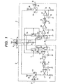
- Fig. 1 is a block diagram to explain a laser drive control circuit, which is an embodiment of the present invention.
- Reference symbol 1 designates a multi-beam laser, 1a a laser diode 1 (LD1), 1b a laser diode 2 (LD2), and 1c a photodiode (PD) for monitoring amounts of light from LD1 and LD2.
- this circuit has an LD1 drive control circuit 2 and an LD2 drive control circuit 3 and is comprised of an initial adjusting resistor Rm1 5 and a fixed resistor Rms 6 which are common to these drive control circuits.
- the initial adjusting resistor Rm1 5 is a resistor capable of being set variably at a desired resistance.
- monitor current 1 switches (SWs) 8a, 8b are selected to the LD1 drive control circuit 2 from a monitor current select signal 7.
- the switch 8b is connected in a switchable state between the fixed resistor Rms 6 and a final adjusting resistor Rm2 9.
- the monitor current (Im) 4 outputted from PD is converted to a monitor voltage (Vm) by the initial adjusting resistor Rm1 5, the LD2 final adjusting resistor Rm2 9, and the fixed resistor Rms 6.
- the initial adjusting resistor 5 and fixed resistor 6 are common resistors used for the adjustment operations of both LD1 and LD2.
- the monitor voltage is then sent to a control means having at least a gain amplifier (amplifying means) 10, a comparator (comparing means) 12, and a reference voltage generating means 11.
- the monitor voltage is amplified by the gain amplifier 10 and thereafter is inputted into the comparator 12 to be compared with the reference voltage a (Vref) of the reference voltage generator 11.
- Numeral 13 denotes a sample-hold circuit, which charges a hold capacitor 15 when the reference voltage a 11 is greater than the monitor voltage (Vm) in sampling according to a sample-hold signal 14, but discharges the hold capacitor 15 otherwise.
- the voltage appearing at the hold capacitor 15 is inputted into a drive amplifier 16 to cause the current set by a drive current setting resistor 18 to flow into the collector of a drive transistor 17.
- a switching transistor 19 When a switching transistor 19 is turned on by a laser modulation signal 21, it allows the current from the laser diode 1 of 1a to flow, thereby effecting emission of light. Since the operation of the LD2 drive control circuit 3 is similar to that of the LD1 drive control circuit 2 except that monitor current 2 switches (SWs) 25a, 25b are selected to the LD2 drive control circuit 3 from the monitor current select signal 7, the description thereof is omitted herein.
- SWs monitor current 2 switches
- numeral 24 represents an inverter, 25 monitor current 2 switches (SWs), 26 an LD2 final adjusting resistor Rm2', 27 a gain amplifier b, 28 a reference voltage b, 29 a comparator b, 30 a sample-hold circuit b, 31 a sample-hold signal b, 32 a sample-hold capacitor b, 33 a drive amplifier b, 34 a drive transistor b, 35 a drive current setting resistor b, 36 a switching transistor b, 37 a load resistor drive transistor b, 38 a laser modulation signal b, 39 a differential driver b, and 40 a laser load resistor.
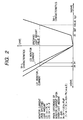
- Fig. 2 is a graph to show the laser drive current lop-emitted light amount L characteristics and the monitor current Im-emitted light amount L characteristics.
- the graph to show the Iop-L characteristics is illustrated on the right side of the axis of L [mW] indicating the emitted light amount L, and the graph to show the Im-L characteristics on the left side of the axis of L [mW].
- the relations of current values Iop, Im to emitted light amount L can be approximated each to a linear function.
- a total set resistance (Rm, Rm') of the adjusting resistors for each of the laser diode 1 and the laser diode 2 is determined uniquely from the reference voltage value Vref and each monitor current value (Im or Im').
- LD1 total set resistance Rm Rm1 + Rm2 + Rms
- LD2 total set resistance Rm' Rm1 + Rm2' + Rms
- maximums are set for the total set resistances of the adjusting resistors. These maximums need to be set so as to be not less than the resistance at the minimum specified light amount.
- Immax, Im'max represent the monitor currents at the maximum specified light amount.
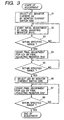
- Fig. 3 is a flowchart to show the adjusting method. The method will be described herein with an example of the adjusting method using LD1 for the initial adjustment.
- the LD1 monitor current Im is selected by the monitor current switch SW (S1).
- the initial adjustment is started to adjust the initial adjusting resistor Rm1 into the specified range; if it is off the specified range it will be adjusted so as to be within the specified range (S2, S3).
- the adjustment is focused into the final specified range by the LD1 final adjusting resistor Rm2; if the resistance is off the final specified range the resistance will be adjusted into the final specified range (S4, S5).
- the monitor current switches (SWs) are turned to the LD2 side (S6). Since the initial adjustment has already been completed in the steps S2, S3 and can be omitted herein, the final adjustment of LD2 is carried out by the LD2 final adjusting resistor Rm2', thereby completing the adjustment (S7, S8).
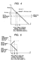
- Fig. 4 is a graph to show the relationship between angle step and resistance.
- variable resistors of a rotating type which rotate in steps of equal angles, are used as the adjusting resistors.
- an effective rotation angle (full rotation angle) capable of outputting a resistance is represented by ⁇ and a rotation angle upon the initial adjustment (initial adjustment rotation angle) and a rotation angle upon the final adjustment (final adjustment rotation angle) by ⁇ int and ⁇ end, respectively.
- a moving angle in each adjustment will be called an angle step.
- Each adjusting resistor can be varied stepwise by an equal amount both upon the initial adjustment and upon the final adjustment.
- Angle steps during the respective adjustments will be called an initial angle step ⁇ S1 and a final angle step ⁇ S2.
- Initial angle step ⁇ S1 ⁇ int/ ⁇
- Final angle step ⁇ S2 ⁇ end/ ⁇
- the initial angle step may be set greater than the final angle step.
- the steps may be set so as to satisfy ⁇ S1 > ⁇ S2.
- a resistance resolution ⁇ RmINT in the initial adjustment (i.e., a change amount of resistance per single angular change) can be expressed as follows from the set maximum Rm1max of the initial adjusting resistor and the initial angle step ⁇ S1.
- ⁇ RmINT Rm1max• ⁇ S1
- the resistance resolution ⁇ RmEND in the final adjustment of LD1 is expressed as follows from the total resistance Rm2max of the final adjusting resistor and the final angle step ⁇ S2.
- ⁇ RmEND Rm2max• ⁇ S2
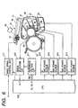
- Fig. 6 is a diagram to show the sectional structure of an image recording apparatus as an embodiment of the present invention and the structure of a density control device installed therein.
- numeral 61 denotes a color image-forming unit of the electrophotographic method
- 62 a photosensitive drum onto which laser beams are guided to form a latent image
- 63 a transfer drum for transferring an image developed from the latent image onto a recording sheet.
- Numeral 64 designates a laser scanning unit for emitting the laser light indicating an image signal.
- Numeral 60 represents a light source unit for emitting multiple beams, described previously, which has at least the laser diodes 1, 2, the photodiode (PD), the LD1 drive control circuit 2, and the LD2 drive control circuit 3 illustrated in Fig. 1.
- Numeral 70 denotes a polygon mirror and 71 a reflecting mirror. The light source unit 60 may also be set in the laser scanning unit 64.
- Numeral 65 indicates a developing unit for yellow toner which develops a yellow latent image
- 66 a developing unit for cyan toner
- 67 a developing unit for magenta toner
- 68 a developing unit for black toner
- Numeral 69 stands for a density sensor unit for detecting the density of an image formed on the photosensitive drum 62
- 610 for a detecting circuit for detecting a density sensor signal from the density sensor unit 69
- 611 for a reference voltage circuit for supplying the reference voltage to the signal detecting circuit 610.
- Numeral 612 designates a CPU (central processing unit) for executing the control of the whole of this apparatus.
- numeral 613 represents a development bias power supply for the yellow developing unit 65, 614 a development bias power supply for the cyan developing unit 66, 615 a development bias power supply for the magenta developing unit 67, and 616 a development bias power supply for the black developing unit 68.
- the sensitive drum 62 After charged by a charging unit not illustrated, is exposed to the laser light beams emitted form the laser diodes 1 and 2 and projected from the laser scanning unit 64.
- the multi-laser beams from the laser scanning unit 64 form a latent image on the surface of the photosensitive drum 62.
- the light amounts of the respective multi-laser beams are approximately equal.
- the yellow development bias power supply 613 is actuated to apply the development bias to the yellow developing unit 65 to visualize the yellow latent image with toner.
- the toner image thus visualized is attracted by transfer high-voltage power applied to the transfer drum 63, whereby it is transferred from the photosensitive drum 62 onto the transfer drum 63.
- the above sequential operation is carried out similarly for each of the colors (yellow Y, magenta M, cyan C, and black Bk), whereby a color image is formed on the transfer drum 63. After that, the color image is transferred onto a transfer sheet (not illustrated) and is then fixed to be printed out.
- the print sequences of the respective colors are independent of each other in the image recording apparatus, so that the toner densities of the respective colors can be detected by measuring the image on the photosensitive drum 62 or on the transfer drum 63 by the density sensor 69. Then toner compounding capable of achieving the optimum image quality can be implemented by controlling the recording condition (the bias herein) in each of the recording processes, using this detection result.
- the toner image transferred onto the photosensitive drum 62 is measured by a reflected light amount measuring system including the density sensor 69 and densities of the respective color toners are always combined stably.
- the present invention presents the effects of work saving of the adjusting circuits and reduction of the adjustment time in the drive control circuits of the multi-beam laser.
- the number of laser beams needs to be increased, for example to 4, in order to further enhance the quality of image, and the effects of work saving and reduction of the adjustment time become further outstanding in such cases.
Landscapes
- Physics & Mathematics (AREA)
- Condensed Matter Physics & Semiconductors (AREA)
- General Physics & Mathematics (AREA)
- Electromagnetism (AREA)
- Optics & Photonics (AREA)
- Laser Beam Printer (AREA)
- Semiconductor Lasers (AREA)
- Mechanical Optical Scanning Systems (AREA)
- Facsimile Scanning Arrangements (AREA)
- Fax Reproducing Arrangements (AREA)
Applications Claiming Priority (4)
| Application Number | Priority Date | Filing Date | Title |
|---|---|---|---|
| JP33445698 | 1998-11-25 | ||
| JP33445698 | 1998-11-25 | ||
| JP11328281A JP2000218865A (ja) | 1998-11-25 | 1999-11-18 | レ―ザ駆動装置とその駆動方法及びそれを用いた画像形成装置 |
| JP32828199 | 1999-11-18 |
Publications (3)
| Publication Number | Publication Date |
|---|---|
| EP1005121A2 EP1005121A2 (en) | 2000-05-31 |
| EP1005121A3 EP1005121A3 (en) | 2002-10-16 |
| EP1005121B1 true EP1005121B1 (en) | 2004-10-06 |
Family
ID=26572811
Family Applications (1)
| Application Number | Title | Priority Date | Filing Date |
|---|---|---|---|
| EP99123349A Expired - Lifetime EP1005121B1 (en) | 1998-11-25 | 1999-11-23 | Laser driving apparatus, driving method thereof, and image-forming apparatus using it |
Country Status (4)
| Country | Link |
|---|---|
| US (1) | US6560256B1 (enExample) |
| EP (1) | EP1005121B1 (enExample) |
| JP (1) | JP2000218865A (enExample) |
| DE (1) | DE69920850T2 (enExample) |
Families Citing this family (20)
| Publication number | Priority date | Publication date | Assignee | Title |
|---|---|---|---|---|
| US6330324B1 (en) * | 1997-12-09 | 2001-12-11 | Sbc Technology Resources, Inc. | Geographical call routing for a non-emergency calling service |
| JP2001244555A (ja) * | 2000-03-01 | 2001-09-07 | Pioneer Electronic Corp | 自動電力制御回路 |
| US6801556B2 (en) * | 2001-11-09 | 2004-10-05 | Agere Systems Inc. | Optical source driver with output load detection circuit |
| US7022960B2 (en) * | 2002-02-12 | 2006-04-04 | Konica Corporation | Photographic film image reading apparatus with film density detection |
| DE10229234A1 (de) * | 2002-06-28 | 2004-02-12 | Deutsche Thomson-Brandt Gmbh | Eigensicherer Pickup für Wiedergabe- oder Aufzeichnungsgeräte unterschiedlicher optischer Aufzeichnungsträger |
| JP2004103839A (ja) * | 2002-09-10 | 2004-04-02 | Canon Inc | 半導体マルチビームレーザ装置及び画像形成装置 |
| CN100389364C (zh) | 2003-03-03 | 2008-05-21 | 佳能株式会社 | 频率调制装置以及频率调制方法 |
| JP4308812B2 (ja) * | 2005-10-28 | 2009-08-05 | 日本テキサス・インスツルメンツ株式会社 | 発光素子駆動装置 |
| JP4214490B2 (ja) * | 2006-08-29 | 2009-01-28 | ブラザー工業株式会社 | レーザ光の出力制御装置、並びに画像形成装置 |
| US7891570B2 (en) * | 2007-02-28 | 2011-02-22 | Microvision, Inc. | Photodiode with improved performance in ambient light |
| TWI367692B (en) * | 2007-09-21 | 2012-07-01 | Aussmak Optoelectronic Corp | Light emitting device and control method thereof |
| US20110080533A1 (en) * | 2009-10-06 | 2011-04-07 | Microvision, Inc. | Dithering Laser Drive Apparatus |
| CN102473428B (zh) * | 2010-06-13 | 2014-12-10 | 联发科技(新加坡)私人有限公司 | 减少apc电路的输入端的数量的方法以及相关apc电路 |
| JP5818495B2 (ja) | 2011-04-21 | 2015-11-18 | キヤノン株式会社 | 画像形成装置 |
| JP6178641B2 (ja) | 2013-06-28 | 2017-08-09 | キヤノン株式会社 | 光走査装置及び画像形成装置 |
| US10496004B2 (en) | 2015-08-20 | 2019-12-03 | Canon Kabushiki Kaisha | Image forming apparatus with current-controlled light emitting element |
| JP6609144B2 (ja) | 2015-09-10 | 2019-11-20 | キヤノン株式会社 | 光走査装置 |
| JP6671931B2 (ja) | 2015-11-16 | 2020-03-25 | キヤノン株式会社 | 画像形成装置 |
| JP2017219714A (ja) | 2016-06-08 | 2017-12-14 | キヤノン株式会社 | 光走査装置 |
| JP6976695B2 (ja) * | 2017-03-08 | 2021-12-08 | 株式会社東芝 | 発光基板、プリントヘッドおよび画像形成装置 |
Family Cites Families (16)
| Publication number | Priority date | Publication date | Assignee | Title |
|---|---|---|---|---|
| JPS56140477A (en) * | 1980-04-02 | 1981-11-02 | Ricoh Co Ltd | Laser driving control system |
| JP2644722B2 (ja) | 1985-03-29 | 1997-08-25 | キヤノン株式会社 | 画像形成装置 |
| US4985896A (en) * | 1985-03-29 | 1991-01-15 | Canon Kabushiki Kaisha | Laser driving device |
| JPS62227667A (ja) | 1986-03-31 | 1987-10-06 | Canon Inc | レ−ザ駆動制御装置 |
| JPS6446724A (en) | 1987-08-17 | 1989-02-21 | Canon Kk | Image recorder |
| JPH06103765B2 (ja) | 1987-10-30 | 1994-12-14 | 日本電気株式会社 | 半導体レーザバイアス電流制御方式 |
| EP0464813B1 (en) * | 1990-07-05 | 1998-10-07 | Canon Kabushiki Kaisha | Driving IC for driving a light source and laser printer using such driving IC |
| US5504517A (en) | 1991-04-04 | 1996-04-02 | Canon Kabushiki Kaisha | Laser scanner control circuit which is used in image forming apparatus and driver IC for use in such a circuit |
| JP3168710B2 (ja) | 1992-07-17 | 2001-05-21 | 松下電器産業株式会社 | パワー制御回路を備えたレーザアレイ |
| US5822343A (en) * | 1994-08-26 | 1998-10-13 | Psc Inc. | Operating and control system for lasers useful in bar code scanners |
| JPH08116114A (ja) | 1994-10-17 | 1996-05-07 | Fuji Xerox Co Ltd | 光量制御装置 |
| US5726437A (en) * | 1994-10-27 | 1998-03-10 | Fuji Xerox Co., Ltd. | Light intensity control device |
| JP3677915B2 (ja) | 1997-01-22 | 2005-08-03 | 富士ゼロックス株式会社 | 光量制御装置 |
| JP4235275B2 (ja) * | 1998-01-09 | 2009-03-11 | キヤノン株式会社 | 画像形成装置 |
| US6055252A (en) * | 1998-09-10 | 2000-04-25 | Photonic Solutions, Inc. | Fiberoptic transmitter using thermistor to maintain stable operating conditions over a range of temperature |
| JP4148485B2 (ja) * | 1998-10-05 | 2008-09-10 | キヤノン株式会社 | 画像形成装置、及び複写機 |
-
1999
- 1999-11-18 JP JP11328281A patent/JP2000218865A/ja active Pending
- 1999-11-23 US US09/447,285 patent/US6560256B1/en not_active Expired - Lifetime
- 1999-11-23 DE DE69920850T patent/DE69920850T2/de not_active Expired - Lifetime
- 1999-11-23 EP EP99123349A patent/EP1005121B1/en not_active Expired - Lifetime
Also Published As
| Publication number | Publication date |
|---|---|
| DE69920850D1 (de) | 2004-11-11 |
| US6560256B1 (en) | 2003-05-06 |
| DE69920850T2 (de) | 2005-02-10 |
| EP1005121A2 (en) | 2000-05-31 |
| EP1005121A3 (en) | 2002-10-16 |
| JP2000218865A (ja) | 2000-08-08 |
Similar Documents
| Publication | Publication Date | Title |
|---|---|---|
| EP1005121B1 (en) | Laser driving apparatus, driving method thereof, and image-forming apparatus using it | |
| US5966395A (en) | Semiconductor laser drive device and image recording device | |
| US4796265A (en) | Imaging using collectively controlled multiple beams | |
| US5504517A (en) | Laser scanner control circuit which is used in image forming apparatus and driver IC for use in such a circuit | |
| JPS62124576A (ja) | 半導体レ−ザの出力調整装置 | |
| US4771431A (en) | Semiconductor laser drive | |
| US6989520B2 (en) | Emission control apparatus with settable target intensity and image forming apparatus using same | |
| US5973719A (en) | Laser scanning unit having automatic power control function | |
| US5408483A (en) | Laser beam emitting device with selective laser beam power output level | |
| US9964887B2 (en) | Light scanning apparatus and image forming apparatus | |
| US5608747A (en) | Thermal cross-talk compensating current driver for laser diode array | |
| US5859659A (en) | Laser beam scanning device and method including light intensity adjustment | |
| US4862466A (en) | Laser emitting apparatus with temperature intensity control | |
| JP4356958B2 (ja) | 画像形成装置及び該装置におけるレーザ駆動制御方法 | |
| US5126761A (en) | Scanning beam output control device for an image recorder | |
| JP2000187374A (ja) | 画像形成装置 | |
| US7403215B2 (en) | Current driver and power control for electrophotographic devices | |
| US5450118A (en) | Image forming apparatus | |
| US6574447B2 (en) | Laser beam emission control for electrophotographic device | |
| JP2004009492A (ja) | 画像形成装置におけるレーザ駆動回路 | |
| EP0841598A2 (en) | Laser light amount control device and image recording apparatus using the device | |
| KR100247985B1 (ko) | 인쇄기의광주사시스템 | |
| JP3681097B2 (ja) | 画像形成装置 | |
| JPH08289155A (ja) | 画像形成装置 | |
| JP2005268286A (ja) | 光ビーム発光制御装置 |
Legal Events
| Date | Code | Title | Description |
|---|---|---|---|
| PUAI | Public reference made under article 153(3) epc to a published international application that has entered the european phase |
Free format text: ORIGINAL CODE: 0009012 |
|
| AK | Designated contracting states |
Kind code of ref document: A2 Designated state(s): AT BE CH CY DE DK ES FI FR GB GR IE IT LI LU MC NL PT SE |
|
| AX | Request for extension of the european patent |
Free format text: AL;LT;LV;MK;RO;SI |
|
| PUAL | Search report despatched |
Free format text: ORIGINAL CODE: 0009013 |
|
| AK | Designated contracting states |
Kind code of ref document: A3 Designated state(s): AT BE CH CY DE DK ES FI FR GB GR IE IT LI LU MC NL PT SE |
|
| AX | Request for extension of the european patent |
Free format text: AL;LT;LV;MK;RO;SI |
|
| RIC1 | Information provided on ipc code assigned before grant |
Free format text: 7H 01S 5/042 A, 7H 01S 5/0683 B, 7H 04N 1/00 B, 7H 01S 5/40 B |
|
| 17P | Request for examination filed |
Effective date: 20030228 |
|
| 17Q | First examination report despatched |
Effective date: 20030410 |
|
| AKX | Designation fees paid |
Designated state(s): DE FR GB IT |
|
| GRAP | Despatch of communication of intention to grant a patent |
Free format text: ORIGINAL CODE: EPIDOSNIGR1 |
|
| GRAS | Grant fee paid |
Free format text: ORIGINAL CODE: EPIDOSNIGR3 |
|
| GRAA | (expected) grant |
Free format text: ORIGINAL CODE: 0009210 |
|
| AK | Designated contracting states |
Kind code of ref document: B1 Designated state(s): DE FR GB IT |
|
| PG25 | Lapsed in a contracting state [announced via postgrant information from national office to epo] |
Ref country code: IT Free format text: LAPSE BECAUSE OF FAILURE TO SUBMIT A TRANSLATION OF THE DESCRIPTION OR TO PAY THE FEE WITHIN THE PRESCRIBED TIME-LIMIT;WARNING: LAPSES OF ITALIAN PATENTS WITH EFFECTIVE DATE BEFORE 2007 MAY HAVE OCCURRED AT ANY TIME BEFORE 2007. THE CORRECT EFFECTIVE DATE MAY BE DIFFERENT FROM THE ONE RECORDED. Effective date: 20041006 Ref country code: FR Free format text: LAPSE BECAUSE OF NON-PAYMENT OF DUE FEES Effective date: 20041006 |
|
| REG | Reference to a national code |
Ref country code: GB Ref legal event code: FG4D |
|
| REG | Reference to a national code |
Ref country code: IE Ref legal event code: FG4D |
|
| REF | Corresponds to: |
Ref document number: 69920850 Country of ref document: DE Date of ref document: 20041111 Kind code of ref document: P |
|
| PLBE | No opposition filed within time limit |
Free format text: ORIGINAL CODE: 0009261 |
|
| STAA | Information on the status of an ep patent application or granted ep patent |
Free format text: STATUS: NO OPPOSITION FILED WITHIN TIME LIMIT |
|
| 26N | No opposition filed |
Effective date: 20050707 |
|
| EN | Fr: translation not filed | ||
| PGFP | Annual fee paid to national office [announced via postgrant information from national office to epo] |
Ref country code: GB Payment date: 20171130 Year of fee payment: 19 |
|
| PGFP | Annual fee paid to national office [announced via postgrant information from national office to epo] |
Ref country code: DE Payment date: 20180131 Year of fee payment: 19 |
|
| REG | Reference to a national code |
Ref country code: DE Ref legal event code: R119 Ref document number: 69920850 Country of ref document: DE |
|
| GBPC | Gb: european patent ceased through non-payment of renewal fee |
Effective date: 20181123 |
|
| PG25 | Lapsed in a contracting state [announced via postgrant information from national office to epo] |
Ref country code: DE Free format text: LAPSE BECAUSE OF NON-PAYMENT OF DUE FEES Effective date: 20190601 |
|
| PG25 | Lapsed in a contracting state [announced via postgrant information from national office to epo] |
Ref country code: GB Free format text: LAPSE BECAUSE OF NON-PAYMENT OF DUE FEES Effective date: 20181123 |