EP1003354B1 - Method of manufacturing organic el display - Google Patents
Method of manufacturing organic el display Download PDFInfo
- Publication number
- EP1003354B1 EP1003354B1 EP99939247A EP99939247A EP1003354B1 EP 1003354 B1 EP1003354 B1 EP 1003354B1 EP 99939247 A EP99939247 A EP 99939247A EP 99939247 A EP99939247 A EP 99939247A EP 1003354 B1 EP1003354 B1 EP 1003354B1
- Authority
- EP
- European Patent Office
- Prior art keywords
- layer
- film
- organic
- display device
- cathode
- Prior art date
- Legal status (The legal status is an assumption and is not a legal conclusion. Google has not performed a legal analysis and makes no representation as to the accuracy of the status listed.)
- Expired - Lifetime
Links
Images


Classifications
-
- H—ELECTRICITY
- H05—ELECTRIC TECHNIQUES NOT OTHERWISE PROVIDED FOR
- H05B—ELECTRIC HEATING; ELECTRIC LIGHT SOURCES NOT OTHERWISE PROVIDED FOR; CIRCUIT ARRANGEMENTS FOR ELECTRIC LIGHT SOURCES, IN GENERAL
- H05B33/00—Electroluminescent light sources
- H05B33/10—Apparatus or processes specially adapted to the manufacture of electroluminescent light sources
-
- H—ELECTRICITY
- H10—SEMICONDUCTOR DEVICES; ELECTRIC SOLID-STATE DEVICES NOT OTHERWISE PROVIDED FOR
- H10K—ORGANIC ELECTRIC SOLID-STATE DEVICES
- H10K50/00—Organic light-emitting devices
- H10K50/80—Constructional details
- H10K50/805—Electrodes
- H10K50/82—Cathodes
-
- H—ELECTRICITY
- H10—SEMICONDUCTOR DEVICES; ELECTRIC SOLID-STATE DEVICES NOT OTHERWISE PROVIDED FOR
- H10K—ORGANIC ELECTRIC SOLID-STATE DEVICES
- H10K59/00—Integrated devices, or assemblies of multiple devices, comprising at least one organic light-emitting element covered by group H10K50/00
- H10K59/10—OLED displays
- H10K59/17—Passive-matrix OLED displays
-
- H—ELECTRICITY
- H10—SEMICONDUCTOR DEVICES; ELECTRIC SOLID-STATE DEVICES NOT OTHERWISE PROVIDED FOR
- H10K—ORGANIC ELECTRIC SOLID-STATE DEVICES
- H10K71/00—Manufacture or treatment specially adapted for the organic devices covered by this subclass
- H10K71/10—Deposition of organic active material
- H10K71/18—Deposition of organic active material using non-liquid printing techniques, e.g. thermal transfer printing from a donor sheet
-
- H—ELECTRICITY
- H10—SEMICONDUCTOR DEVICES; ELECTRIC SOLID-STATE DEVICES NOT OTHERWISE PROVIDED FOR
- H10K—ORGANIC ELECTRIC SOLID-STATE DEVICES
- H10K59/00—Integrated devices, or assemblies of multiple devices, comprising at least one organic light-emitting element covered by group H10K50/00
- H10K59/30—Devices specially adapted for multicolour light emission
- H10K59/35—Devices specially adapted for multicolour light emission comprising red-green-blue [RGB] subpixels
-
- H—ELECTRICITY
- H10—SEMICONDUCTOR DEVICES; ELECTRIC SOLID-STATE DEVICES NOT OTHERWISE PROVIDED FOR
- H10K—ORGANIC ELECTRIC SOLID-STATE DEVICES
- H10K71/00—Manufacture or treatment specially adapted for the organic devices covered by this subclass
-
- H—ELECTRICITY
- H10—SEMICONDUCTOR DEVICES; ELECTRIC SOLID-STATE DEVICES NOT OTHERWISE PROVIDED FOR
- H10K—ORGANIC ELECTRIC SOLID-STATE DEVICES
- H10K71/00—Manufacture or treatment specially adapted for the organic devices covered by this subclass
- H10K71/10—Deposition of organic active material
- H10K71/12—Deposition of organic active material using liquid deposition, e.g. spin coating
- H10K71/13—Deposition of organic active material using liquid deposition, e.g. spin coating using printing techniques, e.g. ink-jet printing or screen printing
- H10K71/135—Deposition of organic active material using liquid deposition, e.g. spin coating using printing techniques, e.g. ink-jet printing or screen printing using ink-jet printing
-
- H—ELECTRICITY
- H10—SEMICONDUCTOR DEVICES; ELECTRIC SOLID-STATE DEVICES NOT OTHERWISE PROVIDED FOR
- H10K—ORGANIC ELECTRIC SOLID-STATE DEVICES
- H10K71/00—Manufacture or treatment specially adapted for the organic devices covered by this subclass
- H10K71/50—Forming devices by joining two substrates together, e.g. lamination techniques
-
- H—ELECTRICITY
- H10—SEMICONDUCTOR DEVICES; ELECTRIC SOLID-STATE DEVICES NOT OTHERWISE PROVIDED FOR
- H10K—ORGANIC ELECTRIC SOLID-STATE DEVICES
- H10K71/00—Manufacture or treatment specially adapted for the organic devices covered by this subclass
- H10K71/60—Forming conductive regions or layers, e.g. electrodes
- H10K71/611—Forming conductive regions or layers, e.g. electrodes using printing deposition, e.g. ink jet printing
-
- H—ELECTRICITY
- H10—SEMICONDUCTOR DEVICES; ELECTRIC SOLID-STATE DEVICES NOT OTHERWISE PROVIDED FOR
- H10K—ORGANIC ELECTRIC SOLID-STATE DEVICES
- H10K85/00—Organic materials used in the body or electrodes of devices covered by this subclass
- H10K85/10—Organic polymers or oligomers
- H10K85/111—Organic polymers or oligomers comprising aromatic, heteroaromatic, or aryl chains, e.g. polyaniline, polyphenylene or polyphenylene vinylene
- H10K85/114—Poly-phenylenevinylene; Derivatives thereof
-
- H—ELECTRICITY
- H10—SEMICONDUCTOR DEVICES; ELECTRIC SOLID-STATE DEVICES NOT OTHERWISE PROVIDED FOR
- H10K—ORGANIC ELECTRIC SOLID-STATE DEVICES
- H10K85/00—Organic materials used in the body or electrodes of devices covered by this subclass
- H10K85/10—Organic polymers or oligomers
- H10K85/111—Organic polymers or oligomers comprising aromatic, heteroaromatic, or aryl chains, e.g. polyaniline, polyphenylene or polyphenylene vinylene
- H10K85/115—Polyfluorene; Derivatives thereof
-
- H—ELECTRICITY
- H10—SEMICONDUCTOR DEVICES; ELECTRIC SOLID-STATE DEVICES NOT OTHERWISE PROVIDED FOR
- H10K—ORGANIC ELECTRIC SOLID-STATE DEVICES
- H10K85/00—Organic materials used in the body or electrodes of devices covered by this subclass
- H10K85/30—Coordination compounds
-
- H—ELECTRICITY
- H10—SEMICONDUCTOR DEVICES; ELECTRIC SOLID-STATE DEVICES NOT OTHERWISE PROVIDED FOR
- H10K—ORGANIC ELECTRIC SOLID-STATE DEVICES
- H10K85/00—Organic materials used in the body or electrodes of devices covered by this subclass
- H10K85/30—Coordination compounds
- H10K85/321—Metal complexes comprising a group IIIA element, e.g. Tris (8-hydroxyquinoline) gallium [Gaq3]
- H10K85/324—Metal complexes comprising a group IIIA element, e.g. Tris (8-hydroxyquinoline) gallium [Gaq3] comprising aluminium, e.g. Alq3
-
- H—ELECTRICITY
- H10—SEMICONDUCTOR DEVICES; ELECTRIC SOLID-STATE DEVICES NOT OTHERWISE PROVIDED FOR
- H10K—ORGANIC ELECTRIC SOLID-STATE DEVICES
- H10K85/00—Organic materials used in the body or electrodes of devices covered by this subclass
- H10K85/60—Organic compounds having low molecular weight
- H10K85/631—Amine compounds having at least two aryl rest on at least one amine-nitrogen atom, e.g. triphenylamine
Definitions
- the present invention relates to a method for manufacturing an organic EL display device which is used in emissive simple matrix drive-type medium or large volume monochromatic or color displays, camcorder or digital camera view finders, and the like.
- the structure of most conventional organic EL elements comprises a transparent electrode formed on a glass substrate, where light is transmitted through the glass substrate.
- the penetration through the glass substrate results in outgoing radiation, and thus in greater light leakage in the direction of the substrate plane, allowing only 20% of the total light emission to be used.
- Japanese Patent Publication No. 10208881 discloses forming a first electrode layer on a transparent board. Then forming a donor film comprising a basic film coated with a light absorbing layer and a transfer layer, The donor film is separated from the transparent board by a predetermined space.
- An object of the present invention is to provide a method for the extremely simple patterning of electrodes and light emitting layers in methods for manufacturing organic EL display devices, and to provide such a method in which all the light emission is radiated outward in the direction of the visual field without being wasted.
- the method for manufacturing an organic EL display device in the present invention is a method for manufacturing an organic EL display device which is used in simple matrix drives, characterised in that a light-heat conversion layer and heat-propagating layer are formed on a film, a cathode layer is then formed, a light emitting layer is then formed thereon, a positive hole-injecting layer is then formed thereon, the film on which these multiple layers have been formed is then placed in contact with a substrate with a stripe-patterned ITO, the aforementioned multiple layers are transferred onto the substrate by irradiating the other side of the film with a laser in such a way as to form the shape of the cathode, the film is then removed, a drive mechanism is connected to the substrate onto which the aforementioned multiple layers have been transferred, and a sealing process is carried out.
- This structure allows cathodes which are extremely unstable and difficult to pattern to be readily patterned simultaneously with the transfer of the organic EL layer by laser.
- the method for manufacturing an organic EL display device in the present invention is a method for manufacturing an organic EL display device which is used in simple matrix drives, characterized in that a light-heat conversion layer and heat-propagating layer are formed on a film, a cathode layer is then formed, an electroluminescent adhesive layer is the formed thereon, the film on which these multiple layers have been formed is then placed in contact with a substrate with a stripe-patterned ITO, the aforementioned multiple layers are transferred onto the substrate by irradiating the other side of the film with a laser in such a way as to form the shape of the cathode, the film is then removed, a drive mechanism connected to the substrate onto which the multiple layers have been transferred, and a sealing process is carried out.
- This structure allows cathodes with a simple structure, which are extremely unstable and difficult to pattern, to be readily patterned simultaneously with the transfer of the organic EL layer by laser.
- Means 3 for solving the problem This is characterized in that an electron-injecting layer is formed between the cathode layer and light emitting layer of the first means for solving the problem or between the cathode layer and the electroluminescent adhesive layer of the second means for solving the problem. This allows the luminous efficiency to be improved in the aforementioned structures.
- Means 4 for solving the problem The method for manufacturing an organic EL display device that is used in simple matrix drives is characterized in that a light-heat conversion layer and heat-propagating layer are formed on a film, an anode layer is then formed, a positive hole-injecting layer is then formed thereon, a light emitting layer is then formed thereon, an electron-injecting adhesive layer is then formed thereon, the film on which these tiple layers have been formed is then placed in contact with a substrate with a patterned cathode, the other side of the film is irradiated with a laser in such a way as to form the shape of the cathode, the film is then removed, a drive mechanism is connected to the substrate onto which the aforementioned multiple layers have been transferred, and a sealing process is carried out.
- This structure allows cathodes which are difficult to pattern to be readily patterned by means of a laser or the like after being formed on a glass substrate, and also allows anodes to be patterned simultaneously during the subsequent transfer of the organic EL layer. This structure also allows light to be directly transmitted to the outside without passing through the glass substrate from the organic light emitting layer, so that no light is lost, resulting in better brightness.
- Means 5 for solving the problem The method for manufacturing an organic EL display device that is used in simple matrix drives is characterized in that a light-heat conversion layer and heat-propagating layer are formed on a film, an anode layer is then formed, a positive hole-injecting layer is then formed thereon, an electroluminescent adhesive layer is then formed thereon, the film on which these multiple layers have been formed is then placed in contact with a substrate with a patterned cathode, the other side of the film is irradiated with a laser in such a way as to form the shape of the cathode, the film is then removed, a drive mechanism is connected to the substrate onto which the aforementioned multiple layers have been transferred, and a sealing process is carried out.
- This structure allows cathodes which are difficult to pattern to be readily patterned by means of a laser or the like after being formed on a glass substrate, and also allows anodes to be patterned simultaneously during the subsequent transfer of the organic EL layer.
- the manufacturing process is also simplified because the adhesive layer also has a light-emitting function.
- This structure also allows light to be directly transmitted to the outside without passing through the glass substrate from the organic light emitting layer, so that no light is lost, resulting in better brightness.
- Means 6 for solving the problem is characterized in that the aforementioned light emitting layer or electroluminescent adhesive layer is formed by applying luminescent substances emitting different-colored light by means of an ink jet head. This means allows different-colored light emitting layers to be readily formed on the film, thereby allowing a colored simple matrix display to be produced with extreme ease.
- Means 7 for solving the problem This is characterized in that means for ink separation between color regions is implemented before said light emitting layer or electroluminescent adhesive layer is applied by an ink jet head. This allows the light emitting layer to be formed in the form of stripes without staining adjacent picture elements
- This embodiment is an example of a method for manufacturing an organic EL display device that is used in simple matrix drives, wherein a light-heat conversion layer and heat-propagating layer are formed on a film, a cathode layer is then formed, a light emitting layer is then formed thereon, a positive hole-injecting layer is then formed thereon, the film on which these multiple layers have been formed is then placed in contact with a substrate with a stripe-patterned ITO, the aforementioned multiple layers are transferred onto the substrate by irradiating the other side of the film with a laser in such a way as to form the shape of the cathode, the film is then removed, a drive mechanism is connected to the substrate onto which the aforementioned multiple layers have been transferred, and a sealing process is carried out.
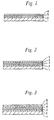
- Figs. 1 through 6 are simple cross sections depicting the method for manufacturing the organic EL display device in the present invention.
- thermosetting epoxy resin in which carbon particles had been mixed was coated to a thickness of 5 microns and cured at room temperature as a layer 2 for converting laser light to heat on a base film 1 comprising a 0.1 mm thick polyethylene terephthalate film.
- a poly- - methylstyrene film was formed when coated to a thickness of 1 micron as a heat propagating and releas layer 3, and aluminum:lithium (10:1) was deposited to a thickness of 200 nm as a cathode layer 4 on the surface (Fig. 1).
- Alq3 was then deposited to a thickness of 70 nm as the light emitting layer (Fig. 2).
- a mixture of NPD and polyvinyl carbazol was then dissolved in solvent, and was coated and dried to a thickness of 60 nm as the positive hole-injecting adhesive layer 6 (Fig. 3).
- the resulting film was then placed in contact with a transparent glass substrate 8 with a patterned ITO having 256 stripes (Fig. 4).
- a pattern of 64 stripes was then produced with a 13 W YAG laser 9 on the film side so as to intersect the striped pattern of the ITO (Fig. 5).
- Drivers 14 and 15 and a controller 16 were then connected to the organic EL substrate 11, as shown in Fig. 7, a transparent protective substrate was placed in contact with UV setting sealant 13, and the protective substrate was cured and sealed by irradiation with UV rays. Moving image display could thus be achieved with the input of drive power and signals to the display device thus obtained.
- General resins such as polycarbonates and polyether sulfones can also be used in addition to polyesters as the transfer film used in this embodiment.
- Any material that can efficiently convert laser light to heat may similarly be used in addition to carbon-kneaded resins as the material for the light-heat conversion layer used in this embodiment.
- Any low melting point (preferably around 100°C) material capable of withstanding the production of heat during the formation of the electrodes can similarly be used in addition to those indicated here as the heat propagating layer used in this embodiment.
- Aluminum, lithium, magnesium, calcium, alloys thereof, halogenated compounds, and the like can be used as the material for forming the cathode in this embodiment.
- Metal complexes such as quinoline, metal complexes such as azomethine, conjugated low molecule weight species and conjugated high molecular weight species or any other such organic EL materials can be used as the light-emitting material used in this embodiment.
- the method for forming the film is not limited to deposition.
- the film can also be formed when the material is coated after being dissolved in a solvent.
- any material capable of injecting positive holes into the light emitting layer such as triphenylamine derivatives, porphin compounds, polyaniline and its derivatives, and polythiophene and its derivatives, can be used in addition to NPD as the positive hole-injecting material used in this embodiment.
- Any resin that does not hamper positive hole injection, that can be melted by heat from laser light, and that has excellent adhesion on ITO and glass can be used as the material used for the adhesive layer in this embodiment.
- Thermosetting resins other than UV setting resin can similarly be used as the sealant used in this embodiment.
- This embodiment is an example of a method for manufacturing an organic EL display device that is used in simple matrix drives, wherein a light-heat conversion layer and heat-propagating layer are formed on a film, a cathode layer is then formed, an electroluminescent adhesive layer is then formed thereon, the film on which these multiple layers have been formed is then placed in contact with a substrate with a stripe-patterned ITO, the aforementioned multiple layers are transferred onto the substrate by irradiating the other side of the film with a laser in such a way as to form the shape of the cathode, the film is then removed, a drive mechanism is connected to the substrate onto which the multiple layers have been transferred, and a sealing process is carried out.
- a light-heat conversion layer and heat propagating layer cathode were first formed on a base film in the same manner as in the first embodiment, and MEH-PPV was made into a film in the form of a chloroform solution and dried to a thickness of 70 nm as the electroluminescent adhesive layer.
- the resulting film was then placed contact with a transparent glass substrate with a patterned ITO in the same manner as in the first embodiment, and a driver circuit was mounted and sealed, giving an organic EL display device.
- Moving image display could thus be achieved with the input of drive power and signals to the display device thus obtained.
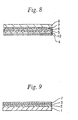
- This embodiment is an example of an electron-injecting layer formed between the cathode and light emitting layer in the first embodiment.
- Fig. 8 is a simple dross section of the organic EL display device in this embodiment.
- Znq2 was deposited to a thickness of 20 nm as an electron-injecting layer 10.
- the light emitting layer and other layers thereafter were then formed in the same manner as in Embodiment 1, giving an organic EL display device.
- the organic EL display device in Embodiment 1 had a luminous efficiency of 21 m/W, whereas this embodiment had a luminous efficiency of 2.51 m/W.
- any material capable of positive hole injection such as polyphenylene vinylene derivatives, organometal complexes such as Alq3, and the like, can be used in addition to NPD as the electron-injecting material used in this embodiment.
- Any method that does not penetrate the cathode can be used as the method for forming the film.
- This embodiment can similarly be used in Embodiment 2.
- This embodiment is an example of a method for manufacturing an organic EL display device that is used in simple matrix drives, wherein a light-heat conversion layer and heat-propagating layer are formed on a film, an anode layer is then formed, a positive hole-injecting layer is then formed thereon, a light emitting layer is then formed thereon, an electron-injecting adhesive layer is then formed thereon, the film on which these multiple layers have been formed is then placed in contact with a substrate with a patterned cathode, the other side of the film is irradiated with a laser in such a way as to form the shape of the cathode, the film is then removed, a drive mechanism is connected to the substrate onto which the aforementioned multiple layers have been transferred, and a sealing process is carried out.
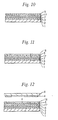
- Figs. 9 through 14 are simple cross sections depicting the method for manufacturing the organic EL display device in the present invention.
- the light-heat conversion layer 2 and heat propagating layer 3 given in Embodiment 1 were formed on a base film 1 comprising a 1 mm thick polycarbonate film, and indium tin oxide was formed by sputtering to a thickness of 200 nm as an anode layer 7 (Fig. 9). was then deposited to a thickness of 15 as the positive hole-injecting layer 17, and NPD was then deposited to a thickness of 20 nm. Alq3 was then deposited to a thickness of 70 nm as the light emitting layer 5 (Fig. 10).
- a chloroform solution of PPV was then applied to a thickness of 60 nm as an electron-injecting adhesive layer 18 (Fig. 11).
- the resulting film was then placed in contact with a transparent glass substrate having an aluminum and lithium alloy cathode patterned with 256 stripes laser (Fig. 12).
- a pattern of 64 stripes was then produced with W YAG laser 9 on the film side so as to intersect the striped pattern of the ITO (Fig. 13).
- a transparent protective substrate was placed in contact with an epoxy thermosetting sealant, and the protective substrate was cured and sealed at room temperature. Moving image display could thus be achieved with the input of drive power and signals to the display device thus obtained.
- the luminous efficiency was 31 m/W.
- Embodiment 1 The same materials and methods given in Embodiment 1 can be used in this embodiment as well.
- This embodiment is an example of a method for manufacturing an organic EL display device that is used in simple matrix drives, wherein a light-heat conversion layer and heat-propagating layer are formed on a film, an anode layer is then formed, a positive hole-injecting layer is then formed thereon, an electroluminescent adhesive layer is then formed thereon, the film on which these multiple layers have been formed is then placed in contact with a substrate with a patterned cathode, the other side of the film is irradiated with a laser in such a way as to form the shape of the cathode, the film is then removed, a drive mechanism is connected to the substrate onto which the aforementioned multiple layers have been transferred, and a sealing process is carried out.
- Figs. 15 through 18 are simple cross sections depicting the method for manufacturing the organic EL display device in the present invention.
- An anode and positive hole-injecting layer were formed on a base film in the same manner as in Embodiment 3.
- a chloroform solution of PPV was then coated and dried to a thickness of 60 nm as an electroluminescent adhesive layer 19 (Fig. 15).
- the resulting film was then placed in contact with a transparent glass substrate 8 having an aluminum and lithium alloy cathode 4 patterned with 256 stripes by laser (Fig. 16).
- a pattern of 64 stripes was then produced with a 13 W YAG laser 9 on the film side so as to intersect the striped pattern of the ITO (Fig. 17).
- a transparent protective substrate was placed in contact with a UV setting sealant, and the protective substrate was cured and sealed at room temperature by being irradiated with UV rays from behind. Moving image display could thus be achieved with the input of drive power and signals to the display device thus obtained.
- the luminous efficiency was 3.51 m/W.
- Embodiment 1 The same materials and methods given in Embodiment 1 can be used in this embodiment as well.
- This embodiment is an example of luminescent substances emitting red, green, and blue light, which are dissolved and applied using an ink jet head to form the aforementioned light emitting layer during the formation of the light emitting layer in Embodiment 4.
- Figs. 19 through 25 are simple cross sections depicting the method for manufacturing the organic EL display device in the present invention.
- a xylene solution of MEH-PPV was applied and dried in the form of a stripe by an ink jet head 20 to form a red-light emitting layer 21.
- a xylene solution of PPV was applied and dried in the form of a stripe by the ink jet head to form a green light emitting layer 22 next to the above layer.
- a xylene solution of a fluorene compound was applied and dried in the form of a stripe by the ink jet head to form a blue light emitting layer 23 between the aforementioned MEH-PPV and PPV derivatives.
- the resulting film was then placed in contact with a transparent glass substrate 8 having an aluminum and lithium alloy cathode 4 patterned with 256 stripes by laser, where the stripes of the light emitting layers were aligned with the stripes of the cathode (Fig. 23).
- a pattern of 64 stripes was then produced with a YAG laser 7 on the film side so as to intersect the striped pattern of the cathode 2 (Fig. 24).
- Embodiment 4 The same materials and manufacturing conditions given in Embodiment 4 can be used in this embodiment as well.
- This embodiment was carried out with the structure given in Embodiment 4, but it can similarly be applied in the preparation of the light emitting layers or electroluminescent adhesive layers in the other embodiments.
- This embodiment is an example of the formation of partition walls in the light emitting layer prior to the formation of the cathode on the film.
- partition walls 24 were printed in the widthwise direction between the colored light emitting layers by means of screen printing using thermosetting polyimide, and were heated and cured on the film used in Embodiment 5.
- An organic EL display device was then obtained in the same manner as in Embodiment 6.
- partition walls are not limited to those given here. Any other material and method capable of manufacturing the structure depicted in Fig. 26 can be used.
- ink may also be applied between picture elements following the formation of the electrode.
- the elemental structure can be the reverse of conventional structures, making it possible to suppress the loss of light that is caused by the effects of moving light when emitted light passes through a glass substrate.
- An organic EL display with high luminous efficiency can thus be inexpensively produced by a simple method.
Abstract
Description


Claims (7)
- A method for producing an organic EL display device used in simple matrix drives, wherein said method for producing an organic EL display device is characterised by comprising the steps of:forming a light-heat conversion layer(2) and heat-propagating layer (3) on a film (1);forming a cathode layer (4);forming a light emitting layer (5) thereon;forming a positive hole-injecting layer (6) thereon;placing the film (1) on which these multiple layers have been formed in contact with a substrate (8) with a stripe-patterned ITO;transferring said multiple layers onto the substrate (8) by irradiating the other side of the film (1) with a laser in such a way as to form the shape of the cathode;removing the film (1);connecting the drive mechanism to the substrate (8) onto which said multiple layers have been transferred andcarrying out a sealing process.
- A method for producing an organic EL display device used in simpler matrix drives, wherein said method for producing an organic EL display device is characterised by comprising the steps of:forming a light-heat conversion layer (2) and heat-propagating layer (3) on a film (1);forming a cathode layer (4);forming an electroluminescent adhesive layer thereon;placing the film (1) on which these multiple layers have been formed in contact with a substrate (8) with a stripe-patterned ITO;transferring said multiple layers onto the substrate (8) by irradiating the other side of the film (1) with a laser in such a way as to form the shape of the cathode;removing the film (1);connecting a drive mechanism to the substrate (8) onto which the multiple layers have been transferred; andcarrying out a sealing process.
- The method for manufacturing an organic EL display device according to claim 1 or 2, characterised in that an electron-injecting layer (10) is formed between said cathode layer (4) and said electroluminescent adhesive layer or said light emitting layer (5).
- A method for producing an organic EL display device used in simple matrix drives, wherein said method for producing an organic EL display device is characterised by comprising the steps of:forming a light-heat conversion layer (2) and heat-propagating layer (3) on a film (1);forming an anode layer (7);forming a positive hole-injecting layer (17) thereon;forming a light emitting layer (5) thereon;forming an electron-injecting adhesive layer (18) thereon;placing the film (1) on which these multiple layers have been formed in contact with a substrate (8) with a patterned cathode;irradiating the other side of the film (1) with a laser in such a way as to form the shape of the cathode;removing the film (1);connecting a drive mechanism to the substrate (8) onto which said multiple layers have been transferred; andcarrying out a sealing process.
- A method for producing an organic EL display device used in simple matrix drives, wherein said method for producing an organic EL display device is characterised by comprising the steps of:fonning a light-heat conversion layer (2) and heat-propagating layer (3) on a film (1);forming an anode layer (7);forming a positive hole-injecting layer (17) thereon;forming an electroluminescent adhesive layer thereon;placing the film (1) on which these multiple layers have been formed in contact with a substrate (8) with a patterned cathode;irradiating the other side of the film (1) with a laser in such a way as to form the shape of the cathode;removing the film (1);connecting a drive mechanism to the substrate onto which said multiple layers have been transferred; andcarrying out a sealing process.
- The method for manufacturing an organic EL display device according to claim 1, 2, 4, or 5, characterised in that said light emitting layer (5) or electroluminescent adhesive layer is formed by applying luminescent substances emitting different-colored light by means of an ink jet head.
- The method for manufacturing an organic EL display device according to claim 6, characterised in that means for ink separation between color regions is implemented before said light emitting layer (5) or electroluminescent adhesive layer is applied by an ink jet head.
Priority Applications (1)
| Application Number | Priority Date | Filing Date | Title |
|---|---|---|---|
| EP05077308A EP1624485B1 (en) | 1998-03-09 | 1999-03-09 | Method for manufacturing organic el display device |
Applications Claiming Priority (3)
| Application Number | Priority Date | Filing Date | Title |
|---|---|---|---|
| JP5721498 | 1998-03-09 | ||
| JP05721498A JP4547723B2 (en) | 1998-03-09 | 1998-03-09 | Manufacturing method of organic EL display device |
| PCT/JP1999/001132 WO1999046961A1 (en) | 1998-03-09 | 1999-03-09 | Method of manufacturing organic el display |
Related Child Applications (1)
| Application Number | Title | Priority Date | Filing Date |
|---|---|---|---|
| EP05077308A Division EP1624485B1 (en) | 1998-03-09 | 1999-03-09 | Method for manufacturing organic el display device |
Publications (3)
| Publication Number | Publication Date |
|---|---|
| EP1003354A1 EP1003354A1 (en) | 2000-05-24 |
| EP1003354A4 EP1003354A4 (en) | 2004-05-19 |
| EP1003354B1 true EP1003354B1 (en) | 2005-12-28 |
Family
ID=13049286
Family Applications (2)
| Application Number | Title | Priority Date | Filing Date |
|---|---|---|---|
| EP99939247A Expired - Lifetime EP1003354B1 (en) | 1998-03-09 | 1999-03-09 | Method of manufacturing organic el display |
| EP05077308A Expired - Lifetime EP1624485B1 (en) | 1998-03-09 | 1999-03-09 | Method for manufacturing organic el display device |
Family Applications After (1)
| Application Number | Title | Priority Date | Filing Date |
|---|---|---|---|
| EP05077308A Expired - Lifetime EP1624485B1 (en) | 1998-03-09 | 1999-03-09 | Method for manufacturing organic el display device |
Country Status (5)
| Country | Link |
|---|---|
| EP (2) | EP1003354B1 (en) |
| JP (1) | JP4547723B2 (en) |
| AT (1) | ATE314802T1 (en) |
| DE (2) | DE69929155T2 (en) |
| WO (1) | WO1999046961A1 (en) |
Cited By (1)
| Publication number | Priority date | Publication date | Assignee | Title |
|---|---|---|---|---|
| US9123595B2 (en) | 2001-12-28 | 2015-09-01 | Semiconductor Energy Laboratory Co., Ltd. | Method for fabricating a semiconductor device by bonding a layer to a support with curvature |
Families Citing this family (39)
| Publication number | Priority date | Publication date | Assignee | Title |
|---|---|---|---|---|
| US6165543A (en) * | 1998-06-17 | 2000-12-26 | Nec Corporation | Method of making organic EL device and organic EL transfer base plate |
| US6114088A (en) | 1999-01-15 | 2000-09-05 | 3M Innovative Properties Company | Thermal transfer element for forming multilayer devices |
| DE60027483T2 (en) | 1999-01-15 | 2007-05-03 | 3M Innovative Properties Co., Saint Paul | Material patterning method |
| JP4009923B2 (en) * | 1999-09-30 | 2007-11-21 | セイコーエプソン株式会社 | EL panel |
| US6284425B1 (en) | 1999-12-28 | 2001-09-04 | 3M Innovative Properties | Thermal transfer donor element having a heat management underlayer |
| US6228555B1 (en) | 1999-12-28 | 2001-05-08 | 3M Innovative Properties Company | Thermal mass transfer donor element |
| US6436222B1 (en) * | 2000-05-12 | 2002-08-20 | Eastman Kodak Company | Forming preformed images in organic electroluminescent devices |
| JP2002083691A (en) | 2000-09-06 | 2002-03-22 | Sharp Corp | Active matrix driven organic led display unit and its manufacturing method |
| US6855384B1 (en) | 2000-09-15 | 2005-02-15 | 3M Innovative Properties Company | Selective thermal transfer of light emitting polymer blends |
| US6358664B1 (en) | 2000-09-15 | 2002-03-19 | 3M Innovative Properties Company | Electronically active primer layers for thermal patterning of materials for electronic devices |
| JP2002108250A (en) | 2000-09-29 | 2002-04-10 | Sharp Corp | Active matrix driven self-luminous display device and manufacturing method therefor |
| JP2002190386A (en) * | 2000-12-20 | 2002-07-05 | Daicel Chem Ind Ltd | Material for organic electroluminescent element, and manufacturing method thereof |
| CN1401204A (en) | 2000-12-20 | 2003-03-05 | 大赛璐化学工业株式会社 | Material for organic electroluminescence device and its manufacturing method |
| JP2002222694A (en) | 2001-01-25 | 2002-08-09 | Sharp Corp | Laser processing device and organic electroluminescent display panel using the same |
| JP2002240437A (en) | 2001-02-19 | 2002-08-28 | Sharp Corp | Donor sheet for forming thin film, manufacturing method therefor, and organic electroluminescence element |
| ATE540437T1 (en) | 2001-03-02 | 2012-01-15 | Fujifilm Corp | PRODUCTION METHOD OF AN ORGANIC THIN FILM DEVICE |
| JP2002343565A (en) | 2001-05-18 | 2002-11-29 | Sharp Corp | Manufacturing method of organic led display panel, organic led display panel manufactured by the same, and base film and substrate used for the same |
| JP2002343564A (en) | 2001-05-18 | 2002-11-29 | Sharp Corp | Transfer film and manufacturing method of organic electroluminescence element using the same |
| US6699597B2 (en) | 2001-08-16 | 2004-03-02 | 3M Innovative Properties Company | Method and materials for patterning of an amorphous, non-polymeric, organic matrix with electrically active material disposed therein |
| SG135973A1 (en) * | 2001-08-16 | 2007-10-29 | 3M Innovative Properties Co | Method and materials for patterning of a polymerizable, amorphous matrix with electrically active material disposed therein |
| TWI258317B (en) | 2002-01-25 | 2006-07-11 | Semiconductor Energy Lab | A display device and method for manufacturing thereof |
| US7241512B2 (en) | 2002-04-19 | 2007-07-10 | 3M Innovative Properties Company | Electroluminescent materials and methods of manufacture and use |
| GB0306409D0 (en) | 2003-03-20 | 2003-04-23 | Cambridge Display Tech Ltd | Electroluminescent device |
| JP2005032917A (en) * | 2003-07-10 | 2005-02-03 | Dainippon Printing Co Ltd | Method for manufacturing organic thin film solar cell and transfer sheet |
| GB2412223B (en) * | 2004-03-20 | 2008-10-22 | Hewlett Packard Development Co | Method of applying light filters and busbars to a display substrate |
| JP4970242B2 (en) * | 2004-03-20 | 2012-07-04 | ヒューレット−パッカード デベロップメント カンパニー エル.ピー. | Application of color elements and bus bars to display substrates |
| JP4548153B2 (en) * | 2005-03-07 | 2010-09-22 | セイコーエプソン株式会社 | Manufacturing method of organic EL display device |
| DE102006013834A1 (en) * | 2006-03-23 | 2007-09-27 | Tesa Ag | Electroluminescent PSAs |
| US7670450B2 (en) | 2006-07-31 | 2010-03-02 | 3M Innovative Properties Company | Patterning and treatment methods for organic light emitting diode devices |
| JP4450006B2 (en) | 2007-04-02 | 2010-04-14 | ソニー株式会社 | Substrate for transfer and method for producing organic electroluminescent device |
| JP2009048811A (en) | 2007-08-16 | 2009-03-05 | Sony Corp | Transcription substrate and method for manufacturing organic electroluminescent element |
| US8080811B2 (en) | 2007-12-28 | 2011-12-20 | Semiconductor Energy Laboratory Co., Ltd. | Method for manufacturing evaporation donor substrate and light-emitting device |
| JP4502224B2 (en) * | 2008-01-15 | 2010-07-14 | 大日本印刷株式会社 | Organic EL transfer body provided with pattern transfer layer, organic EL transferred body, and organic EL device manufacturing method |
| WO2009107548A1 (en) | 2008-02-29 | 2009-09-03 | Semiconductor Energy Laboratory Co., Ltd. | Deposition method and manufacturing method of light-emitting device |
| US8182863B2 (en) | 2008-03-17 | 2012-05-22 | Semiconductor Energy Laboratory Co., Ltd. | Deposition method and manufacturing method of light-emitting device |
| KR101629637B1 (en) | 2008-05-29 | 2016-06-13 | 가부시키가이샤 한도오따이 에네루기 켄큐쇼 | Deposition method and method of manufacturing light-emitting device |
| CN104952702B (en) * | 2015-05-15 | 2017-11-28 | 张家港康得新光电材料有限公司 | Semiconductor devices and preparation method thereof |
| CN108878668A (en) * | 2018-07-04 | 2018-11-23 | 京东方科技集团股份有限公司 | Backboard and preparation method thereof, display device and lighting device |
| CN114055970A (en) * | 2020-08-03 | 2022-02-18 | 湖南鼎一致远科技发展有限公司 | Device layer structure capable of being thermally transferred, color tape structure and preparation method thereof |
Family Cites Families (15)
| Publication number | Priority date | Publication date | Assignee | Title |
|---|---|---|---|---|
| JPS61163591A (en) * | 1985-01-11 | 1986-07-24 | 関西日本電気株式会社 | Manufacture of organic type el element |
| JPS642297A (en) * | 1987-06-24 | 1989-01-06 | Nec Kansai Ltd | Manufacture of electroluminescent element |
| JPH06283265A (en) * | 1993-03-25 | 1994-10-07 | Nec Kansai Ltd | Electroluminescent lamp and manufacture thereof and equipment for manufacture thereof |
| JPH0757871A (en) * | 1993-08-19 | 1995-03-03 | Hitachi Ltd | Electroluminescence display device |
| JP3585524B2 (en) * | 1994-04-20 | 2004-11-04 | 大日本印刷株式会社 | Manufacturing method of organic thin film EL element |
| JPH07302685A (en) * | 1994-05-10 | 1995-11-14 | Nec Kansai Ltd | Manufacture of electroluminescent lamp |
| US5563019A (en) * | 1994-06-30 | 1996-10-08 | E. I. Du Pont De Nemours And Company | Donor element for laser-induced thermal transfer |
| US5686383A (en) * | 1995-08-22 | 1997-11-11 | Eastman Kodak Company | Method of making a color filter array by colorant transfer and lamination |
| US5688551A (en) * | 1995-11-13 | 1997-11-18 | Eastman Kodak Company | Method of forming an organic electroluminescent display panel |
| US5766819A (en) * | 1995-11-29 | 1998-06-16 | E. I. Dupont De Nemours And Company | Donor elements, assemblages, and associated processes with flexible ejection layer(s) for laser-induced thermal transfer |
| US5695907A (en) * | 1996-03-14 | 1997-12-09 | Minnesota Mining And Manufacturing Company | Laser addressable thermal transfer imaging element and method |
| JP3036436B2 (en) * | 1996-06-19 | 2000-04-24 | セイコーエプソン株式会社 | Method of manufacturing active matrix type organic EL display |
| US5998085A (en) * | 1996-07-23 | 1999-12-07 | 3M Innovative Properties | Process for preparing high resolution emissive arrays and corresponding articles |
| KR100195175B1 (en) * | 1996-12-23 | 1999-06-15 | 손욱 | Electroluminescence element and its manufacturing method |
| JP3466876B2 (en) * | 1997-06-16 | 2003-11-17 | キヤノン株式会社 | Manufacturing method of electroluminescence device |
-
1998
- 1998-03-09 JP JP05721498A patent/JP4547723B2/en not_active Expired - Lifetime
-
1999
- 1999-03-09 WO PCT/JP1999/001132 patent/WO1999046961A1/en active IP Right Grant
- 1999-03-09 EP EP99939247A patent/EP1003354B1/en not_active Expired - Lifetime
- 1999-03-09 EP EP05077308A patent/EP1624485B1/en not_active Expired - Lifetime
- 1999-03-09 DE DE69929155T patent/DE69929155T2/en not_active Expired - Lifetime
- 1999-03-09 AT AT99939247T patent/ATE314802T1/en not_active IP Right Cessation
- 1999-03-09 DE DE69938800T patent/DE69938800D1/en not_active Expired - Lifetime
Cited By (3)
| Publication number | Priority date | Publication date | Assignee | Title |
|---|---|---|---|---|
| US9123595B2 (en) | 2001-12-28 | 2015-09-01 | Semiconductor Energy Laboratory Co., Ltd. | Method for fabricating a semiconductor device by bonding a layer to a support with curvature |
| US9337341B2 (en) | 2001-12-28 | 2016-05-10 | Semiconductor Energy Laboratory Co., Ltd. | Semiconductor device having aluminum-containing layer between two curved substrates |
| US9536901B2 (en) | 2001-12-28 | 2017-01-03 | Semiconductor Energy Laboratory Co., Ltd. | Method for fabricating a semiconductor device by bonding a layer to a support with curvature |
Also Published As
| Publication number | Publication date |
|---|---|
| DE69929155T2 (en) | 2006-08-24 |
| JPH11260549A (en) | 1999-09-24 |
| ATE314802T1 (en) | 2006-01-15 |
| DE69929155D1 (en) | 2006-02-02 |
| EP1003354A1 (en) | 2000-05-24 |
| EP1003354A4 (en) | 2004-05-19 |
| EP1624485A2 (en) | 2006-02-08 |
| DE69938800D1 (en) | 2008-07-03 |
| JP4547723B2 (en) | 2010-09-22 |
| EP1624485B1 (en) | 2008-05-21 |
| WO1999046961A1 (en) | 1999-09-16 |
| EP1624485A3 (en) | 2006-11-29 |
Similar Documents
| Publication | Publication Date | Title |
|---|---|---|
| EP1003354B1 (en) | Method of manufacturing organic el display | |
| US6091196A (en) | Organic electroluminescent display device and method of manufacture thereof | |
| JP3902938B2 (en) | Organic light emitting device manufacturing method, organic light emitting display manufacturing method, organic light emitting device, and organic light emitting display | |
| JP3861400B2 (en) | Electroluminescent device and manufacturing method thereof | |
| JP3900724B2 (en) | Organic EL element manufacturing method and organic EL display device | |
| KR100588440B1 (en) | Organic Electroluminescent Device and Method for Producing it | |
| US20020001026A1 (en) | Production of organic luminescence device | |
| GB2391686A (en) | Electroluminescent display | |
| JPH10153967A (en) | Full-color organic el display device and its production | |
| JP2003264083A (en) | Organic led element and production process thereof | |
| JPH1187063A (en) | Electroluminescent element | |
| JP5092485B2 (en) | Organic electroluminescence display and manufacturing method thereof | |
| JP2000195675A (en) | Substrate for organic electroluminescent display element and organic electroluminescent display element | |
| KR20110111429A (en) | Display panel producing method and substrate for display device | |
| US20110175522A1 (en) | Substrate for patterned application and organic el element | |
| JP2000036391A (en) | Organic electroluminescent element and manufacture thereof | |
| JPH1187062A (en) | Electroluminescent element | |
| JP3674848B2 (en) | Organic thin film light emitting display and method for manufacturing the same | |
| JP4548153B2 (en) | Manufacturing method of organic EL display device | |
| JP2003317949A (en) | Manufacturing method for organic el element | |
| JP2001195012A (en) | Organic electroluminescence display device and method for manufacturing the same | |
| WO2002087287A1 (en) | Electroluminescence display panel, image display, and method for manufacturing them | |
| JP5292863B2 (en) | Organic electroluminescent display device and manufacturing method thereof | |
| JP4044362B2 (en) | Manufacturing method of organic EL element | |
| JP2003347054A (en) | Film for thin film transfer, its manufacturing method, and organic el element using same |
Legal Events
| Date | Code | Title | Description |
|---|---|---|---|
| PUAI | Public reference made under article 153(3) epc to a published international application that has entered the european phase |
Free format text: ORIGINAL CODE: 0009012 |
|
| 17P | Request for examination filed |
Effective date: 20000315 |
|
| AK | Designated contracting states |
Kind code of ref document: A1 Designated state(s): AT BE CH CY DE DK ES FI FR GB GR IE IT LI LU MC NL PT SE |
|
| A4 | Supplementary search report drawn up and despatched |
Effective date: 20040407 |
|
| 17Q | First examination report despatched |
Effective date: 20050120 |
|
| GRAP | Despatch of communication of intention to grant a patent |
Free format text: ORIGINAL CODE: EPIDOSNIGR1 |
|
| GRAS | Grant fee paid |
Free format text: ORIGINAL CODE: EPIDOSNIGR3 |
|
| GRAA | (expected) grant |
Free format text: ORIGINAL CODE: 0009210 |
|
| AK | Designated contracting states |
Kind code of ref document: B1 Designated state(s): AT BE CH CY DE DK ES FI FR GB GR IE IT LI LU MC NL PT SE |
|
| PG25 | Lapsed in a contracting state [announced via postgrant information from national office to epo] |
Ref country code: NL Free format text: LAPSE BECAUSE OF FAILURE TO SUBMIT A TRANSLATION OF THE DESCRIPTION OR TO PAY THE FEE WITHIN THE PRESCRIBED TIME-LIMIT Effective date: 20051228 Ref country code: LI Free format text: LAPSE BECAUSE OF FAILURE TO SUBMIT A TRANSLATION OF THE DESCRIPTION OR TO PAY THE FEE WITHIN THE PRESCRIBED TIME-LIMIT Effective date: 20051228 Ref country code: IT Free format text: LAPSE BECAUSE OF FAILURE TO SUBMIT A TRANSLATION OF THE DESCRIPTION OR TO PAY THE FEE WITHIN THE PRESCRIBED TIME-LIMIT;WARNING: LAPSES OF ITALIAN PATENTS WITH EFFECTIVE DATE BEFORE 2007 MAY HAVE OCCURRED AT ANY TIME BEFORE 2007. THE CORRECT EFFECTIVE DATE MAY BE DIFFERENT FROM THE ONE RECORDED. Effective date: 20051228 Ref country code: FI Free format text: LAPSE BECAUSE OF FAILURE TO SUBMIT A TRANSLATION OF THE DESCRIPTION OR TO PAY THE FEE WITHIN THE PRESCRIBED TIME-LIMIT Effective date: 20051228 Ref country code: CH Free format text: LAPSE BECAUSE OF FAILURE TO SUBMIT A TRANSLATION OF THE DESCRIPTION OR TO PAY THE FEE WITHIN THE PRESCRIBED TIME-LIMIT Effective date: 20051228 Ref country code: BE Free format text: LAPSE BECAUSE OF FAILURE TO SUBMIT A TRANSLATION OF THE DESCRIPTION OR TO PAY THE FEE WITHIN THE PRESCRIBED TIME-LIMIT Effective date: 20051228 Ref country code: AT Free format text: LAPSE BECAUSE OF FAILURE TO SUBMIT A TRANSLATION OF THE DESCRIPTION OR TO PAY THE FEE WITHIN THE PRESCRIBED TIME-LIMIT Effective date: 20051228 |
|
| REG | Reference to a national code |
Ref country code: GB Ref legal event code: FG4D |
|
| REG | Reference to a national code |
Ref country code: CH Ref legal event code: EP |
|
| REG | Reference to a national code |
Ref country code: IE Ref legal event code: FG4D |
|
| REF | Corresponds to: |
Ref document number: 69929155 Country of ref document: DE Date of ref document: 20060202 Kind code of ref document: P |
|
| PG25 | Lapsed in a contracting state [announced via postgrant information from national office to epo] |
Ref country code: IE Free format text: LAPSE BECAUSE OF NON-PAYMENT OF DUE FEES Effective date: 20060309 |
|
| PG25 | Lapsed in a contracting state [announced via postgrant information from national office to epo] |
Ref country code: SE Free format text: LAPSE BECAUSE OF FAILURE TO SUBMIT A TRANSLATION OF THE DESCRIPTION OR TO PAY THE FEE WITHIN THE PRESCRIBED TIME-LIMIT Effective date: 20060328 Ref country code: GR Free format text: LAPSE BECAUSE OF FAILURE TO SUBMIT A TRANSLATION OF THE DESCRIPTION OR TO PAY THE FEE WITHIN THE PRESCRIBED TIME-LIMIT Effective date: 20060328 Ref country code: DK Free format text: LAPSE BECAUSE OF FAILURE TO SUBMIT A TRANSLATION OF THE DESCRIPTION OR TO PAY THE FEE WITHIN THE PRESCRIBED TIME-LIMIT Effective date: 20060328 |
|
| PG25 | Lapsed in a contracting state [announced via postgrant information from national office to epo] |
Ref country code: MC Free format text: LAPSE BECAUSE OF NON-PAYMENT OF DUE FEES Effective date: 20060331 Ref country code: LU Free format text: LAPSE BECAUSE OF NON-PAYMENT OF DUE FEES Effective date: 20060331 |
|
| PG25 | Lapsed in a contracting state [announced via postgrant information from national office to epo] |
Ref country code: ES Free format text: LAPSE BECAUSE OF FAILURE TO SUBMIT A TRANSLATION OF THE DESCRIPTION OR TO PAY THE FEE WITHIN THE PRESCRIBED TIME-LIMIT Effective date: 20060408 |
|
| PG25 | Lapsed in a contracting state [announced via postgrant information from national office to epo] |
Ref country code: PT Free format text: LAPSE BECAUSE OF FAILURE TO SUBMIT A TRANSLATION OF THE DESCRIPTION OR TO PAY THE FEE WITHIN THE PRESCRIBED TIME-LIMIT Effective date: 20060529 |
|
| NLV1 | Nl: lapsed or annulled due to failure to fulfill the requirements of art. 29p and 29m of the patents act | ||
| REG | Reference to a national code |
Ref country code: CH Ref legal event code: PL |
|
| ET | Fr: translation filed | ||
| PLBE | No opposition filed within time limit |
Free format text: ORIGINAL CODE: 0009261 |
|
| STAA | Information on the status of an ep patent application or granted ep patent |
Free format text: STATUS: NO OPPOSITION FILED WITHIN TIME LIMIT |
|
| 26N | No opposition filed |
Effective date: 20060929 |
|
| REG | Reference to a national code |
Ref country code: IE Ref legal event code: MM4A |
|
| PG25 | Lapsed in a contracting state [announced via postgrant information from national office to epo] |
Ref country code: CY Free format text: LAPSE BECAUSE OF FAILURE TO SUBMIT A TRANSLATION OF THE DESCRIPTION OR TO PAY THE FEE WITHIN THE PRESCRIBED TIME-LIMIT Effective date: 20051228 |
|
| REG | Reference to a national code |
Ref country code: FR Ref legal event code: TQ Ref country code: FR Ref legal event code: CD Ref country code: FR Ref legal event code: CA |
|
| REG | Reference to a national code |
Ref country code: DE Ref legal event code: R081 Ref document number: 69929155 Country of ref document: DE Owner name: SEIKO EPSON CORP., JP Free format text: FORMER OWNERS: SEIKO EPSON CORP., TOKYO, JP; MINNESOTA MINING AND MANUFACTURING COMPANY, ST. PAUL, MINN., US Effective date: 20110505 Ref country code: DE Ref legal event code: R081 Ref document number: 69929155 Country of ref document: DE Owner name: 3M INNOVATIVE PROPERTIES CO., ST. PAUL, US Free format text: FORMER OWNERS: SEIKO EPSON CORP., TOKYO, JP; MINNESOTA MINING AND MANUFACTURING COMPANY, ST. PAUL, MINN., US Effective date: 20110505 Ref country code: DE Ref legal event code: R081 Ref document number: 69929155 Country of ref document: DE Owner name: 3M INNOVATIVE PROPERTIES CO., ST. PAUL, US Free format text: FORMER OWNER: SEIKO EPSON CORP., MINNESOTA MINING AND MANUFACTUR, , US Effective date: 20110505 Ref country code: DE Ref legal event code: R081 Ref document number: 69929155 Country of ref document: DE Owner name: 3M INNOVATIVE PROPERTIES CO., US Free format text: FORMER OWNER: SEIKO EPSON CORP., MINNESOTA MINING AND MANUFACTUR, , US Effective date: 20110505 Ref country code: DE Ref legal event code: R081 Ref document number: 69929155 Country of ref document: DE Owner name: SEIKO EPSON CORP., JP Free format text: FORMER OWNER: SEIKO EPSON CORP., MINNESOTA MINING AND MANUFACTUR, , US Effective date: 20110505 |
|
| REG | Reference to a national code |
Ref country code: FR Ref legal event code: PLFP Year of fee payment: 18 |
|
| REG | Reference to a national code |
Ref country code: FR Ref legal event code: PLFP Year of fee payment: 19 |
|
| REG | Reference to a national code |
Ref country code: FR Ref legal event code: PLFP Year of fee payment: 20 |
|
| PGFP | Annual fee paid to national office [announced via postgrant information from national office to epo] |
Ref country code: DE Payment date: 20180322 Year of fee payment: 20 Ref country code: GB Payment date: 20180307 Year of fee payment: 20 |
|
| PGFP | Annual fee paid to national office [announced via postgrant information from national office to epo] |
Ref country code: FR Payment date: 20180323 Year of fee payment: 20 |
|
| REG | Reference to a national code |
Ref country code: DE Ref legal event code: R071 Ref document number: 69929155 Country of ref document: DE |
|
| REG | Reference to a national code |
Ref country code: GB Ref legal event code: PE20 Expiry date: 20190308 |
|
| PG25 | Lapsed in a contracting state [announced via postgrant information from national office to epo] |
Ref country code: GB Free format text: LAPSE BECAUSE OF EXPIRATION OF PROTECTION Effective date: 20190308 |