EP1003330B1 - Imaging system - Google Patents
Imaging system Download PDFInfo
- Publication number
- EP1003330B1 EP1003330B1 EP99309147A EP99309147A EP1003330B1 EP 1003330 B1 EP1003330 B1 EP 1003330B1 EP 99309147 A EP99309147 A EP 99309147A EP 99309147 A EP99309147 A EP 99309147A EP 1003330 B1 EP1003330 B1 EP 1003330B1
- Authority
- EP
- European Patent Office
- Prior art keywords
- signal
- pixel
- photo
- exposure period
- time
- Prior art date
- Legal status (The legal status is an assumption and is not a legal conclusion. Google has not performed a legal analysis and makes no representation as to the accuracy of the status listed.)
- Expired - Lifetime
Links
- 238000003384 imaging method Methods 0.000 title claims description 53
- 230000015654 memory Effects 0.000 claims description 109
- 238000000034 method Methods 0.000 claims description 12
- 230000008859 change Effects 0.000 claims description 11
- 230000007423 decrease Effects 0.000 claims description 9
- 230000006870 function Effects 0.000 claims description 6
- 230000010354 integration Effects 0.000 claims description 6
- 230000001419 dependent effect Effects 0.000 claims description 5
- 230000036962 time dependent Effects 0.000 claims 13
- 238000012544 monitoring process Methods 0.000 claims 2
- 230000002457 bidirectional effect Effects 0.000 claims 1
- 230000002401 inhibitory effect Effects 0.000 claims 1
- 239000003990 capacitor Substances 0.000 description 17
- 230000004913 activation Effects 0.000 description 13
- 238000010586 diagram Methods 0.000 description 8
- 230000004044 response Effects 0.000 description 7
- 238000005070 sampling Methods 0.000 description 5
- 230000008901 benefit Effects 0.000 description 4
- 238000005286 illumination Methods 0.000 description 4
- 230000035945 sensitivity Effects 0.000 description 4
- 230000003213 activating effect Effects 0.000 description 3
- 230000009849 deactivation Effects 0.000 description 3
- 239000004065 semiconductor Substances 0.000 description 3
- 238000006243 chemical reaction Methods 0.000 description 2
- 239000002131 composite material Substances 0.000 description 2
- 230000001066 destructive effect Effects 0.000 description 2
- 238000009792 diffusion process Methods 0.000 description 2
- 230000001360 synchronised effect Effects 0.000 description 2
- 238000007796 conventional method Methods 0.000 description 1
- 230000003247 decreasing effect Effects 0.000 description 1
- 230000009977 dual effect Effects 0.000 description 1
- 230000000694 effects Effects 0.000 description 1
- 238000005516 engineering process Methods 0.000 description 1
- 230000003071 parasitic effect Effects 0.000 description 1
- 230000008569 process Effects 0.000 description 1
- 238000004904 shortening Methods 0.000 description 1
Images


Classifications
-
- H—ELECTRICITY
- H01—ELECTRIC ELEMENTS
- H01L—SEMICONDUCTOR DEVICES NOT COVERED BY CLASS H10
- H01L27/00—Devices consisting of a plurality of semiconductor or other solid-state components formed in or on a common substrate
- H01L27/14—Devices consisting of a plurality of semiconductor or other solid-state components formed in or on a common substrate including semiconductor components sensitive to infrared radiation, light, electromagnetic radiation of shorter wavelength or corpuscular radiation and specially adapted either for the conversion of the energy of such radiation into electrical energy or for the control of electrical energy by such radiation
- H01L27/144—Devices controlled by radiation
- H01L27/146—Imager structures
- H01L27/14643—Photodiode arrays; MOS imagers
-
- H—ELECTRICITY
- H04—ELECTRIC COMMUNICATION TECHNIQUE
- H04N—PICTORIAL COMMUNICATION, e.g. TELEVISION
- H04N25/00—Circuitry of solid-state image sensors [SSIS]; Control thereof
- H04N25/50—Control of the SSIS exposure
- H04N25/53—Control of the integration time
- H04N25/533—Control of the integration time by using differing integration times for different sensor regions
-
- H—ELECTRICITY
- H04—ELECTRIC COMMUNICATION TECHNIQUE
- H04N—PICTORIAL COMMUNICATION, e.g. TELEVISION
- H04N25/00—Circuitry of solid-state image sensors [SSIS]; Control thereof
- H04N25/50—Control of the SSIS exposure
- H04N25/57—Control of the dynamic range
- H04N25/571—Control of the dynamic range involving a non-linear response
-
- H—ELECTRICITY
- H04—ELECTRIC COMMUNICATION TECHNIQUE
- H04N—PICTORIAL COMMUNICATION, e.g. TELEVISION
- H04N25/00—Circuitry of solid-state image sensors [SSIS]; Control thereof
- H04N25/70—SSIS architectures; Circuits associated therewith
- H04N25/76—Addressed sensors, e.g. MOS or CMOS sensors
- H04N25/77—Pixel circuitry, e.g. memories, A/D converters, pixel amplifiers, shared circuits or shared components
- H04N25/772—Pixel circuitry, e.g. memories, A/D converters, pixel amplifiers, shared circuits or shared components comprising A/D, V/T, V/F, I/T or I/F converters
Definitions
- the invention relates generally to imaging sensors and more particularly to an imaging sensor utilizing CMOS active pixels having in-pixel local exposure control.
- APSs Active Pixel Sensors
- ADC analog-to-digital converter
- the pixels that are utilized in conventional APSs can be classified into two types of pixels.
- the first type of pixel is commonly referred to as an "analog pixel.”
- An analog pixel includes a photo sensor, such as a photodiode or a phototransistor, and may include an amplifier.
- An associated ADC and memory are located external to the pixel. Therefore, any current generated by the photo sensor of an analog pixel is transmitted from the pixel to the external ADC as an analog signal.
- the second type of pixel is known as a "digital pixel.”
- a digital pixel includes not only a photo sensor and an amplifier, but also an ADC.
- the ADC is contained within the pixel, along with the photo sensor and the amplifier.
- the magnitude of current generated by the photo sensor is digitized within the pixel and can be transferred to off-pixel components as a digital signal.
- the imaging sensor of Fowler et al. has an array of pixels, wherein each pixel includes a phototransistor and an ADC.
- the analog signal generated by the phototransistor is converted to a serial stream of digital data bits by the on-pixel ADC.
- the digital data is then filtered and stored in an external memory.
- the on-pixel ADC is described as having the advantage of minimizing parasitic effects and distortion caused by low signal-to-noise ratio.
- the prior art active pixel sensors operate to image a scene of interest by quantifying the degrees of radiance from various scene segments. For each scene segment, a particular pixel quantifies the degree of radiance from the scene segment by measuring a photo voltage driven by a photo-sensor-generated current.
- a photo sensor When a photo sensor is exposed to incident light from a segment of the scene for a fixed integration or exposure time period, the magnitude of a photo voltage will be dependent upon the intensity of radiance from the scene that is being imaged by the photo sensor.
- Fig. 1 illustrates the technique utilized by the prior art imaging sensors to quantify the intensity of radiance from a scene segment.
- three lines 10, 12 and 14 are plotted with respect to voltage over time.
- the lines 10, 12 and 14 represent photo voltages corresponding to three degrees of radiance from the scene segment that is sensed by a prior art imaging sensor.
- the line 10 represents the voltages over time when the degree of radiance from the scene segment is the maximum level detectable by the imaging sensor.
- the line 14, represents the voltages over time when the degree of radiance from the scene segment is at the minimum level detectable by the imaging sensor.
- the line 12 represents the voltages over time when the degree of radiance from the scene segment is at the mean illumination level.
- the imaging sensor quantifies the magnitude of the photo voltage using an ADC.
- V SAT the degree of radiance from the scene
- the imaging sensor configured to the limits defined by V SAT and V RESET will be able to differentiate discrete degrees of scene radiance that result in a photo voltage between V SAT and V RESET .
- the amount of differentiable degrees of scene radiance that can be detected by an imaging sensor is at least partially dependent on the resolution of the ADC.
- the radiance sensitivity may be adjusted by shortening or extending the length of the fixed exposure period, but the adjustment is a tradeoff of increasing sensitivity of either high radiant scene segments or low radiant scene segments.
- US-A-5,565,915 discloses an image-taking apparatus in which a photosensor is connected to a converter which terminates an image-taking operation in dependence on a particular voltage change rather than after a fixed time.
- the disclosure of this document corresponds generally to the preambles of the independent claims.
- a system and a method for imaging a scene of interest determine a scene segment radiance based upon time periods ("exposure periods") required to achieve a fixed voltage drop.
- sampling data is based on the time required for a set voltage drop (i.e., voltage-driven sampling).
- the voltage-driven sampling occurs at each pixel in a pixel array that is used to provide image information in discrete scene segments.
- the rate of voltage drop corresponds to the intensity of scene segment radiance, such that high radiant scene segments yield more rapid voltage drops than lower radiant scene segments.
- the variable exposure periods are measured for each pixel in the pixel array to gather exposure periods from different segments of the scene being imaged.
- the measured exposure periods are then translated into grayscale information that can be used to generate a composite image having various levels of grayscale that are representative of the imaged scene.
- the variable exposure period is measured within each pixel by comparing the voltage at a floating diffusion (FD) node to a reference voltage.
- the voltages at the FD node and the reference voltage are input to a comparator that outputs a signal when the voltage at the FD node is equal to or less than the reference voltage.
- the FD node is connected to a photo sensor, e.g., photodiode, to generate a photo current in response to incident light from an associated scene segment.
- the generated current causes dissipation of charge from an integration capacitor connected to the FD node, causing the voltage at the FD node to decrease.
- the rate of decrease in voltage at the FD node is accelerated if the magnitude of the photo current is increased. Therefore, the time period for the voltage at the FD node to drop from a reset voltage to the reference voltage is mathematically related to the radiance of the scene segment from which the pixel receives light energy. This time period defines the exposure period for the scene segment being imaged.
- each pixel includes an analog-to-digital converter (ADC) to digitize the duration of the exposure period within the pixel.
- ADC analog-to-digital converter
- the ADC is designed to capture a digital count that is supplied by an off-pixel counter.
- the captured digital count represents the exposure period for the scene segment being imaged.
- the off-pixel counter may be configured to provide non-linear digital counts.
- the non-linear digital counts may be utilized to change the relationship between the exposure period and the degree of radiance from a scene segment.
- a known but non-linear relationship may be established by providing the reference voltage as a non-linear signal.
- the reference voltage may increase with time in order to shorten a potentially long exposure period associated with low radiance scenes.
- Each pixel also includes memory to store the captured digital count.
- the in-pixel memory contains a number of memory cells that can store the captured digital count. Preferably, the number of memory cells is at least as great as the number of bits in the digital count.
- the memory cells are configured such that each memory cell is coupled to a bi-directional bit line.
- the bi-directional bit line functions as both a read bit line and a write bit line for reading and writing operations.
- the memory cells are dual port memory cells having a three-transistor configuration.
- Each memory cell includes a write access transistor, a read access transistor, and a data-controlled transistor.
- the read access transistor and the data-controlled transistor are configured to provide a conductive path from an associated bi-directional bit line to ground.
- the write access transistor connects the bi-directional bit line to the gate of the data-controlled transistor.
- a storage node is located between the write access transistor and the gate of the data-controlled transistor.
- the data stored in the storage node can control the conductive state of the data-controlled transistor.
- the stored data in the storage node is indirectly read by the effect of the conductive state of the data-controlled transistor. Therefore, the stored data is not destroyed during the read operation.
- the non-destructive feature of the memory cell allows less frequent refresh cycles, or no refresh requirement for high speed read-out applications.
- each pixel contains an electronic shutter in which all the pixels simultaneously sense, digitize, and store digital image data in response to a scene being imaged.
- the pixels output digital signals, rather than analog signals.
- the pixels can store the digital image data for an indefinite period, and thereby functions as an image frame buffer.
- Another advantage of the invention is that a greater dynamic range is achieved, which equates to superior imaging performance. Still another advantage is that sensitivity for low radiant scene segments are increased with the use of variable exposure periods. Furthermore, the pixel design is compatible with scaled CMOS technologies with a low supply voltage.
- an imaging sensor in accordance with the present invention measures the duration of a variable exposure time period to determine the degree of radiance from a scene segment.
- the measured exposure period is the time period that is required for a photo-sensor-generated current to discharge from a fixed reset voltage to a fixed reference voltage.
- the reset voltage and the reference voltage are defined as V RESET and V REF , respectively.
- Line 16 represent changes in voltage when the degree of radiance from a scene segment is the maximum level detectable by the present invention
- line 20 represents changes in voltage when the degree of radiance from a scene segment is the minimum level.
- Line 18 represents changes in voltage when the degree of radiance from a scene segment is at the mean illumination of the entire scene to be imaged.
- the slopes of lines 16, 18 and 20 are defined by the magnitude of a photo-sensor-generated current. However, the magnitude of the current is proportional to the degree of radiance from the scene segment.
- the three time periods defined by T 1 , T 2 and T 3 represent the exposure periods for the three degrees of radiance.
- V REF The value of V REF with respect to V RESET affects the performance of the imaging sensor utilizing the variable exposure period technique.
- a high value of V REF or a small change in voltage between V RESET and V REF , will yield a faster photo sensor response time than a low value of V REF .
- the performance of the imaging sensor will be limited by sensor noise and by the maximum counter clock frequency allowed by a digitizer circuitry.
- a low value of V REF will provide a signal that is less degraded by sensor noise, but the sensor response will be slower.
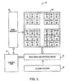
- an imaging system 22 in accordance with the present invention is shown.
- the imaging system 22 is manufactured on a single semiconductor chip.
- the imaging system 22 utilizes the above-described technique of quantifying a variable exposure period to determine the degree of radiance from a scene segment.
- the imaging system 22 includes an array 24 of pixels 25.
- Each pixel 25 is designed to measure an exposure period in response to the degree of radiance from a scene segment and then digitize the measured exposure period.
- each pixel 25 is capable of storing the digitized data that represents the measured exposure period.
- the imaging system 22 further includes a row decoder 26, a read-write-and-refresh (RWR) circuit 28, a column decoder 30, and a control unit 32.
- RWR read-write-and-refresh
- the row decoder 26 is configured to select a row of pixels 25 in the array 24 during a read, write or refresh operation.
- the column decoder 30 operates to select a column of pixels 25 during one of the previously mentioned operations.
- the RWR circuit 28 is designed to direct the flow of data between the pixels 25 and the control unit 32.
- RWR circuit 28 includes circuitry necessary to refresh data stored within the pixels 25.
- the control unit 32 provides the necessary control and timing signals to the RWR circuit 28, the decoders 26 and 30, and the pixels 25.
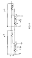
- the imaging pixel circuit 34 having in-pixel local exposure control that can capture, digitize and store image data from a scene of interest is shown.
- the imaging pixel circuit 34 is contained within each of the pixels 25 in the array 24 of Fig. 3 .
- the pixel circuit 34 includes a photodiode 36, a comparator 38, a dynamic buffer memory 40 and supporting circuitry.
- the photodiode 36 is coupled between a P-channel metal-oxide-semiconductor (PMOS) transistor 42 and electrical ground.
- the PMOS transistor 42 functions as a reset switch to connect the photodiode 36 to a V RESET voltage.
- the V RESET voltage is supplied to the PMOS transistor 42 by an external source (not shown).
- a RESET signal applied to the gate of PMOS transistor 42, activates or deactivates the PMOS transistor 42.
- a floating diffusion (FD) node 44 connects the junction of the PMOS transistor 42 and the photodiode 36 to the comparator 38.
- the voltage at the FD node is the critical voltage that will be monitored to determine the exposure period for a scene segment to be imaged.
- an integration capacitor 46 Also connected to FD node 44 is an integration capacitor 46.
- the capacitor 46 is a built-in capacitor that is formed by the devices surrounding the FD node 44.
- the comparator 38 consists of two gate-coupled PMOS transistors 48 and 50 that are connected to a supply voltage VDD.
- a MOS transistor 52 is connected in series with the PMOS transistor 48, while a MOS transistor 54 is connected in series with the PMOS transistor 50.
- the gate of MOS transistor 52 is connected to the FD node 44.
- the gate of MOS transistor 54 is connected to an external circuitry (not shown) to receive a V REF voltage.
- the MOS transistors 52 and 54 are coupled to a MOS transistor 56 such that the transistors 48 and 52 provide a first conductive path from VDD to the transistor 56 and transistors 50 and 54 provide a second conductive path from VDD to the transistor 56.
- the gate of transistor 56 is coupled to the gates of PMOS transistors 48 and 50.
- a transistor 58 connects the transistor 56 to ground.
- the transistor 58 is controlled by a CLK signal, which controls the activation and deactivation of the comparator 38.
- the comparator 38 operates to indicate the voltage at FD node 44 with respect to the V REF voltage. If the voltage at FD node 44 is greater than the V REF voltage, the comparator 38 outputs a high signal at an output terminal 60. When the voltage at FD node 44 is equal to or less than the V REF voltage, the comparator 38 outputs a low signal at the output terminal 60. However, when a low CLK signal is provided to the gate of transistor 58, no current is allowed to flow through the comparator 38, deactivating the comparator 38. The lack of current flow results in a high signal at the output terminal 60, regardless of the voltage at FD node 44. A high CLK signal activates the comparator 38 to monitor the voltage at FD node 44 with respect to the V REF voltage.
- the transistor 62 is a PMOS transistor.
- the gates of transistors 62 and 64 are coupled to the output terminal 60.
- the transistors 62 and 64 are connected in series between VDD and ground.
- the transistor 62 is connected to VDD, while the transistor 64 is connected to ground.
- the transistors 62 and 64 operate to invert a signal on the output terminal 60 and transmit the inverted signal to a gate terminal 66 that is connected to a node between the transistors 62 and 64.
- the inverted signal on the gate terminal 66 can drive a pre-charged high signal on a write word line (WWL) 68 to a low signal, depending upon the inverted signal.
- WWL write word line
- the gate of PMOS transistor 70 is configured to receive the RESET signal to control the conductive state of the PMOS transistor 70.
- the gate of transistor 72 is connected to the gate terminal 66.
- the RESET signal that turns "on” the PMOS transistor 42, pre-charging the voltage at FD node 44 to V RESET , also turns “on” the PMOS transistor 70, pre-charging the voltage at the WWL 68 to VDD.
- the transistor 72 When the voltage at the gate terminal 66 changes from a low signal to a high signal, the transistor 72 is activated. The activation of the transistor 72 drives the high signal on the WWL 68 from the high signal to a low signal. However, a low signal on the gate terminal 66 will not affect the signal on the WWL 68.
- the WWL 68 is coupled to a PMOS transistor 74 that can also connect the WWL 68 to VDD.
- the PMOS transistor 74 is controlled by a word line access (WLA) signal that is supplied to the gate of transistor 74.
- WLA word line access
- Also coupled to the WWL 68 is a transistor 76 that can connect the WWL 68 to ground.
- a write terminate (WT) signal is supplied to the gate of transistor 76 to control the connection of WWL 68 to ground.
- the WLA and WT signals are utilized during refresh and write operations.
- the WWL 68 extends to the dynamic buffer memory 40.
- a number of bi-directional bit lines (BLs) 78 are coupled to the dynamic buffer memory 40.
- the bi-directional BLs 78 are able to carry bits of digital counts from an external counter (not shown) to the dynamic buffer memory 40.
- the bi-directional BLs 78 are configured to carry stored data from the dynamic buffer memory 40 to the RWL circuit 28.
- Contained within the dynamic buffer memory 40 are memory cells that can store digital data, such as a digital count.
- the number of memory cells corresponds to the number of bi-directional BLs 78. As an example, the number of memory cells and bi-directional BLs 78 may be sixteen.
- the dynamic buffer memory 40 is a 16-bit dynamic buffer memory that can store a 16-bit digital count. Also connected to the dynamic buffer memory 40 is a read word line (RWL) 80. The RWL 80 and WWL 68 are connected to the memory cells within the dynamic buffer memory 40 to access the memory cells for retrieval and storage of data.
- the primary function of the dynamic buffer memory 40 is to capture and store a particular digital count when the voltage at FD node 44 has dropped to V REF .
- the captured digital count represents the exposure period that can be used to determine the degree of radiance from a scene segment being imaged.
- the dynamic buffer memory 40 may include sixteen or more memory cells, identical to the memory cells 82 and 84.
- the memory cell 82 is comprised of transistors 86, 88 and 90.
- a storage capacitor 92 is shown to be a component of the memory cell 82 to illustrate the capacitance at a storage node 94.
- the transistor 86 is connected between the bi-directional BL 78 and the storage node 94.
- the gate of transistor 86 is coupled to the WWL 68.
- the transistor 86 is a write access transistor that must be activated to write data into the memory cell 82.
- the transistors 88 and 90 provide a conductive connection from the bi-directional BL 78 to ground.
- the gate of transistor 90 is coupled to the RWL 80, while the gate of transistor 88 is coupled to the storage node 94.
- the conductive state of the transistor 88 is controlled by a bit of data stored in the capacitor 92, when the bi-directional BL 78 is pre-charged to a high signal and the transistor 90 is activated.
- the transistor 90 is a read access transistor that must be activated to read the stored data in the memory cell 82.
- the memory cell 84 is identical to the memory cell 82.
- the memory cell 84 includes transistors 96, 98 and 100 and a storage capacitor 102 at a storage node 104.
- a write operation simply involves transmitting data to be stored through the bi-directional BL 78 and then applying a high signal to the WWL 68, activating the transistor 86.
- a read operation involves pre-charging the bi-directional BL 78 to a high signal and activating the transistor 90.
- the high signal on the bi-directional BL 78 will be either pulled low or maintained high.
- a high signal i.e., a "1” stored in the capacitor 92 will activate the transistor 88 when the transistor 90 is turned “on.”
- the activation of both transistors 88 and 90 connects the bi-directional BL 78 to ground, pulling the high signal on the bi-directional BL 78 to a low signal.
- a low signal i.e., a "0”
- the transistor 88 will not be activated when the transistor 90 is turned “on.”
- the high signal on the bi-directional BL 78 will remain high. Therefore, the signal on the bi-directional BL 78, after the activation of transistor 90, is the inverse of the signal stored in the capacitor 92 as data.
- the memory cells of dynamic buffer memory 40 are dynamic random access memory (DRAM) cells. These memory cells allow the stored data to be read without destroying the stored data in the process, since the stored data is applied only to gates of transistors.
- the non-destructive feature of the memory cells requires less frequent refresh cycles, or no refresh operation for high speed read-out applications. Therefore, the memory cells can be read numerous times without the need to refresh the stored data. However, the memory cells will need to be refreshed at some point if data is stored in the memory cells for a long period of time. Since stored data is read from the memory cells as inverted signals of the stored data in the memory cells, the signals that must be written back into the memory cells must be the inverse of the read signals, i.e., the original stored data.
- DRAM dynamic random access memory
- each memory cell of dynamic buffer memory 40 is connected to a corresponding sense amplifier circuit, such as a sense amplifier circuit 106 shown in Fig. 6 .
- the sense amplifier circuits are included in the RWR circuit 28 of Fig. 3 .
- the sense amplifier circuit 106 will be described as if it is connected to the memory cell 82.
- the sense amplifier circuit 106 includes a weak feedback latch 108, an inverter 110 and transistors 112, 114, 116 and 118.
- the latch 108 is comprised of a large inverter 120 and a smaller inverter 122 on a feedback 124.
- the inverters 120 and 122 operate to hold a signal on an input node 126.
- the latch 108 is connected to a data bus 128.
- the data bus 128 provides an output path for data stored in the memory cell 82 during a read operation.
- the data bus 128 provides an output path from the memory cell 82 to the control unit 32 of Fig. 3 .
- the transistor 118 that is controlled by a BD_gate signal, connects the latch 108 to the data bus 128.
- the latch 108 can also be conductively connected to the bi-directional BL 78 through one of two paths 132 and 134.
- the path 132 is conducting when the transistor 114 is activated by an R_gate signal, whereas, the path 134 is conducting when the transistor 116 is activated by a control write enable (CWE) signal.
- a third path 130 connects the BL 78 to VDD when the transistor 112 is activated by a BLOAD signal.
- the inverter 110 that inverts sensed data from the memory cell 82 back to the original stored data during a refresh operation.
- One of the paths 132 and 134 also provides a connection between the bi-directional BL 78 to a write bit line (WBL) 136.
- the WBL 136 is connected to the external counter to receive digital count data.
- the WBL 136 may be connected to an off-chip external device (not shown) to receive data that is to be written into the memory cell 82.
- the data to be written may be the read-out data from the memory cell 82 that has been modified by the off-chip external device.
- the image capturing operation of the imaging system 22 will be described with reference to Figs. 3-6 .
- the image capturing operation is simultaneously performed within each pixel 25 in the array 24 of Fig. 3 .
- Each pixel 25 performs the image capturing operation in an identical manner.
- V REF is supplied to the comparator 38 of Fig. 4 at the gate of transistor 54.
- the RESET signal is then set low to reset the voltage at FD node 44 to V RESET and the voltage at WWL 68 to VDD.
- the resetting of the voltage at WWL 68 to VDD equates to a high signal on WWL 68, which activates the write access transistors in the memory cells of the dynamic buffer memory 40.
- the RESET signal is switched to a high signal, turning "off" the PMOS transistors 42 and 70, and isolating FD node 44 and the WWL 68.
- the high RESET signal marks the beginning of a variable exposure period for all the pixels 25 in the array 24.
- a high CWE signal is supplied to the transistor 116 of the sense amplifier circuit 106 of Fig. 6 , as well as to all identical transistors of other sense amplifier circuits corresponding to the memory cells of dynamic buffer memory 40.
- the activation of transistor 116 of the sense amplifier circuit 106 and other identical transistors in the corresponding sense amplifier circuits provides conductive connections between the dynamic buffer memory 40 to the external counter via the bi-directional BLs 78.
- the conductive connections allow the external counter to transmit digital counts to the dynamic buffer memory 40.
- the external counter is initiated to sequentially transmit the digital counts at the start of the exposure period.
- the voltage at FD node 44 is V RESET , which is greater than V REF .
- the comparator 38 activated by a high CLK signal, provides a high signal at the output terminal 60.
- the high signal at the output terminal 60 turns “on” the transistor 64 that connects the gate terminal 66 to ground, generating a low signal on the gate terminal.
- the low signal on the gate terminal 66 does not turn “on” the transistor 72.
- the high signal on the WWL 68 remains high.
- the consistent high signal on WWL 68 maintains the conductive state of the write access transistors in the memory cells of the dynamic buffer memory 40. Therefore, the storage capacitors of memory cells are able to receive sequential digital counts from the external counter.
- the imaging pixel circuit 34 will remain in this state until the voltage at FD node 44 drops to V REF .
- the voltage at FD node 44 decreases from V RESET in response to a current generated by the photodiode 36.
- the rate of decrease in voltage at FD node 44 is a function of the intensity of incident light that impinges the photodiode 36.
- the intensity of incident light will vary in accordance to the degree of radiance from a scene of interest.
- the photodiode 36 When the radiance is high, the photodiode 36 generates a large current due to the increase in the intensity of incident light upon the photodiode 36.
- the large current causes the capacitor 46 to discharge, lowering the voltage at FD node 44.
- the photodiode 36 will generate a smaller current. The smaller current also causes the capacitor 46 to discharge and lower the voltage at FD node 44, but at a slower rate.
- the comparator 38 When the voltage at FD node 44 falls to V REF , the comparator 38 generates a low signal to the output terminal 60.
- the low signal at the output terminal 60 deactivates the transistor 64 and activates the PMOS transistor 62.
- the activation of transistor 62 pulls the low signal on the gate terminal 66 to a high signal.
- the high signal on the gate terminal 66 then activates the transistor 72, connecting WWL 68 to ground.
- the high signal on WWL 68 is converted into a low signal, turning “off” the write access transistors in the memory cells of the dynamic buffer memory 40.
- the deactivation of write access transistors "captures" the latest digital count that was transmitted from the external counter.
- the external counter continues to transmit additional digital counts. However, the subsequent digital counts do not affect the captured digital count stored in the dynamic buffer memory 40.
- the image capturing operation is terminated after a predetermined time that is referenced from the start of the exposure period.
- the CLK signal may be held high during the entire period between the start of the exposure period and the termination of the image capturing operation, the CLK signal may be comprised of a series of pulses to decrease power dissipation by the current drain caused by the activation of the comparator 38.
- the CLK signal may be synchronized to a duty cycle, such that the CLK signal is high for a short period in between the times when the digital counts are received by the dynamic buffer memory 40.
- the voltage at FD node 44 will be compared only during these short moments when the comparator 38 is activated.
- the power dissipation of the imaging pixel circuit 34 can be significantly lowered.
- the digital counts that are provided by the external counter are linear counts.
- the V REF that is used to compare the falling voltage at FD node 44 is a constant signal.
- the external counter may be implemented with a non-linear clock period to change the relationship of exposure period and the degree of radiance from a scene of interest.
- the external counter may utilize a logarithmic period to generate logarithmic digital counts. The captured digital count by a pixel will then have a logarithmic relationship with the exposure period, resulting in a more balanced grayscale resolution for the range of radiance intensities of the scene being imaged.
- the V REF may be provided as a non-linear signal.
- the V REF signal may increase with time in order to shorten a potentially long exposure period associated with low radiant scenes.
- a timing diagram for a refresh operation of the imaging system 22 of Fig. 3 is shown.
- the refresh operation will be described with reference to Figs. 3-6 , in addition to Fig. 7 .
- a row of pixels 25 in the array 24 is selected by the row decoder 26 to refresh the memory cells within each pixel of the row.
- a high BLOAD signal is supplied to the transistor 112 in the sense amplifier circuit 106 of Fig. 3 and identical transistors in other sense amplifier circuits that are connected to each memory cell in the selected array row.
- the activation of BLOAD-signal-controlled transistors connects the bi-directional BLs 78 that are associated with the memory cells to VDD, pre-charging the bi-directional BLs high.
- the BLOAD signal drops to a low signal, deactivating the BLOAD-signal-controlled transistors.
- a signal on a read word line such as the RWL 68, is switched to a high signal from a low signal, turning on the read access transistors of the memory cells in the selected array row.
- the activation of read access transistors allows stored data in each memory cell to either pull down the pre-charged high signal on the bi-directional BL 78 to a low signal or leave the high signal unchanged.
- a high signal, i.e., a "1" stored in a memory cell will pull down the high signal on a bi-directional BL to a low signal.
- a low signal i.e., a "0" stored in a memory cell will not change the high signal on a bi-directional BL.
- the resulting signal on the bi-directional BLs 78 reflects the stored data in an inverted form.
- a high R_gate signal is supplied to the transistor 114 and other identical transistors in the sense amplifier circuits, connecting the bi-directional BLs 78 to the weak feedback latches in the sense amplifier circuits.
- the weak feedback latches hold the inverted signals from the bi-directional BLs 78.
- the read access transistors and the R_gate-signal-controlled transistors are deactivated by pulling down the high signal on the read word line and switching the R_gate signal to a low signal.
- the CWE signal is switched from a low signal to a high signal, activating the transistor 116 and other identical transistors in the sense amplifier circuits.
- the inverted signals held by the weak feedback latches are converted to correspond to the original stored data in the memory cells by the inverter 110 and other identical inverters in the sense amplifier circuits.
- the converted signals are transmitted to the bi-directional BLs by the activation of CWE signal controlled transistors.
- the WLA signal is switched from a high signal to a low signal, turning "on” the PMOS transistor 74 of Fig. 4 and other identical PMOS transistors in the selected pixels.
- the activation of WLA-signal-controlled transistors connects the write word lines, such as the WWL 68, to VDD.
- the VDD on write word lines turns "on” the write access transistors in the memory cells of the selected pixels.
- the activation of write access transistors allows the converted signals from the sense amplifier circuits to be written into the memory cells.
- the WLA is switched back to a high signal, disconnecting the write word lines from VDD.
- the CWE signal is pulled low to deactivate the CWE-signal-controlled transistors, isolating the memory cells from the sense amplifier circuits.
- a high WT signal is provided to the transistor 76 and other identical transistors in the pixels, to pull down the high signal on the write word lines to deactivate the write access transistors.
- the WT signal is switched into a low signal, turning "off" the WT-signal-controlled transistors.
- the refresh cycle may be repeated.
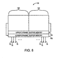
- the pixels 25 of Fig. 3 are configured as pixel pairs that share their pixel spaces to accommodate the two dynamic buffer memories utilized by the two pixels in each pixel pair.
- a pixel pair 138 in accordance to the preferred embodiment is shown.
- the pixel pair 138 includes a left pixel 140 and a right pixel 142.
- the left pixel 140 utilizes an upper dynamic buffer memory 144
- the right pixel 142 utilizes a lower dynamic buffer memory 146.
- Half of the buffer memory 144 is located in the left pixel 140.
- the other half of the buffer memory 144 is located in the right pixel 142.
- the buffer memory 146 is located in both the left and right pixels 140 and 142.
- the reading and writing operation includes sequentially selecting a row of pixels 25 in the array 24 and accessing, in an alternating fashion, the lower dynamic buffer memories and the upper dynamic buffer memories. In this manner, all the pixels 25 in the array 24 can be accessed for retrieval or storage of data.
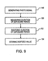
- a photo signal is generated by a photodiode within a particular pixel of the imaging system 22 in response to a radiance from the scene of interest. The degree of radiance determines a magnitude of the photo signal.
- a duration of an exposure period is measured to determine the relative strength of the photo signal. The duration of the exposure period is defined by a fixed decrease in voltage of an exposure signal from a reset voltage to a reference voltage, wherein the rate of decrease is dependent on the magnitude of the photo signal.
- the duration of the exposure period is digitized into a digital value. The digitization of the exposure period duration is preferably performed within the pixel of the imaging system 22.
- the digital value is stored in a memory associated with that pixel. In the preferred embodiment, the memory is located within a pixel array of the imaging system 22.
Landscapes
- Engineering & Computer Science (AREA)
- Physics & Mathematics (AREA)
- Multimedia (AREA)
- Signal Processing (AREA)
- Power Engineering (AREA)
- Condensed Matter Physics & Semiconductors (AREA)
- Electromagnetism (AREA)
- General Physics & Mathematics (AREA)
- Nonlinear Science (AREA)
- Computer Hardware Design (AREA)
- Microelectronics & Electronic Packaging (AREA)
- Transforming Light Signals Into Electric Signals (AREA)
- Solid State Image Pick-Up Elements (AREA)
Applications Claiming Priority (2)
| Application Number | Priority Date | Filing Date | Title |
|---|---|---|---|
| US09/195,588 US6580454B1 (en) | 1998-11-18 | 1998-11-18 | CMOS active pixel sensor having in-pixel local exposure control |
| US195588 | 1998-11-18 |
Publications (2)
| Publication Number | Publication Date |
|---|---|
| EP1003330A1 EP1003330A1 (en) | 2000-05-24 |
| EP1003330B1 true EP1003330B1 (en) | 2009-10-14 |
Family
ID=22721982
Family Applications (1)
| Application Number | Title | Priority Date | Filing Date |
|---|---|---|---|
| EP99309147A Expired - Lifetime EP1003330B1 (en) | 1998-11-18 | 1999-11-17 | Imaging system |
Country Status (4)
| Country | Link |
|---|---|
| US (1) | US6580454B1 (ja) |
| EP (1) | EP1003330B1 (ja) |
| JP (1) | JP4389190B2 (ja) |
| DE (1) | DE69941532D1 (ja) |
Families Citing this family (54)
| Publication number | Priority date | Publication date | Assignee | Title |
|---|---|---|---|---|
| US6977685B1 (en) * | 1999-02-26 | 2005-12-20 | Massachusetts Institute Of Technology | Single-chip imager system with programmable dynamic range |
| KR100306876B1 (ko) * | 1999-10-30 | 2001-11-02 | 박종섭 | 피드백 회로를 구비하여 고속으로 동작하기 위한 이미지 센서 |
| US6671771B2 (en) * | 1999-12-21 | 2003-12-30 | Intel Corporation | Hash CAM having a reduced width comparison circuitry and its application |
| US6452152B1 (en) * | 2000-02-22 | 2002-09-17 | Pixim, Inc. | Sense amplifier having a precision analog reference level for use with image sensors |
| JP4390967B2 (ja) | 2000-04-21 | 2009-12-24 | 富士フイルム株式会社 | 電子カメラ |
| US6985181B2 (en) * | 2000-05-09 | 2006-01-10 | Pixim, Inc. | CMOS sensor array with a memory interface |
| TW518552B (en) * | 2000-08-18 | 2003-01-21 | Semiconductor Energy Lab | Liquid crystal display device, method of driving the same, and method of driving a portable information device having the liquid crystal display device |
| TW514854B (en) * | 2000-08-23 | 2002-12-21 | Semiconductor Energy Lab | Portable information apparatus and method of driving the same |
| US7184014B2 (en) * | 2000-10-05 | 2007-02-27 | Semiconductor Energy Laboratory Co., Ltd. | Liquid crystal display device |
| US6950135B2 (en) * | 2001-01-24 | 2005-09-27 | Hewlett-Packard Development Company, L.P. | Method and apparatus for gathering three dimensional data with a digital imaging system |
| US6747623B2 (en) * | 2001-02-09 | 2004-06-08 | Semiconductor Energy Laboratory Co., Ltd. | Liquid crystal display device and method of driving the same |
| US20020113887A1 (en) * | 2001-02-16 | 2002-08-22 | Iimura Russell M. | CMOS image sensor with extended dynamic range |
| US20040201697A1 (en) * | 2001-05-07 | 2004-10-14 | Vernon Lawrence Klein | "Black-box" video or still recorder for commercial and consumer vehicles |
| TWI273539B (en) * | 2001-11-29 | 2007-02-11 | Semiconductor Energy Lab | Display device and display system using the same |
| JP3913534B2 (ja) * | 2001-11-30 | 2007-05-09 | 株式会社半導体エネルギー研究所 | 表示装置及びこれを用いた表示システム |
| US20030206236A1 (en) * | 2002-05-06 | 2003-11-06 | Agfa Corporation | CMOS digital image sensor system and method |
| US7106367B2 (en) * | 2002-05-13 | 2006-09-12 | Micron Technology, Inc. | Integrated CMOS imager and microcontroller |
| US7256421B2 (en) | 2002-05-17 | 2007-08-14 | Semiconductor Energy Laboratory, Co., Ltd. | Display device having a structure for preventing the deterioration of a light emitting device |
| JP4067878B2 (ja) * | 2002-06-06 | 2008-03-26 | 株式会社半導体エネルギー研究所 | 発光装置及びそれを用いた電気器具 |
| JP4172216B2 (ja) * | 2002-07-16 | 2008-10-29 | ソニー株式会社 | 撮像装置 |
| TWI286436B (en) * | 2003-02-27 | 2007-09-01 | Advmatch Technology Inc | Image sensing device to determine the exposure time automatically |
| CA2443206A1 (en) * | 2003-09-23 | 2005-03-23 | Ignis Innovation Inc. | Amoled display backplanes - pixel driver circuits, array architecture, and external compensation |
| JP3723563B2 (ja) * | 2004-04-07 | 2005-12-07 | 廣津 総吉 | 半導体撮像素子 |
| JP4589131B2 (ja) * | 2005-01-24 | 2010-12-01 | 株式会社フォトロン | 画像センサおよびその画像読み出し方法 |
| US7565077B2 (en) * | 2006-05-19 | 2009-07-21 | Seiko Epson Corporation | Multiple exposure regions in a single frame using a rolling shutter |
| AT504582B1 (de) * | 2006-11-23 | 2008-12-15 | Arc Austrian Res Centers Gmbh | Verfahren zur generierung eines bildes in elektronischer form, bildelement für einen bildsensor zur generierung eines bildes sowie bildsensor |
| US8289430B2 (en) * | 2007-02-09 | 2012-10-16 | Gentex Corporation | High dynamic range imaging device |
| US20090002535A1 (en) * | 2007-06-27 | 2009-01-01 | Arizona Board Of Regents On Behalf Of Arizona State University | Offset-compensated self-reset cmos image sensors |
| US7920193B2 (en) * | 2007-10-23 | 2011-04-05 | Aptina Imaging Corporation | Methods, systems and apparatuses using barrier self-calibration for high dynamic range imagers |
| US8587706B2 (en) | 2008-01-30 | 2013-11-19 | Gentex Corporation | Imaging device |
| US8629927B2 (en) * | 2008-04-09 | 2014-01-14 | Gentex Corporation | Imaging device |
| EP2093996A1 (fr) * | 2008-02-22 | 2009-08-26 | CSEM Centre Suisse d'Electronique et de Microtechnique SA Recherche et Développement | Capteur de vision pour la mésure d'invariants tels les contrastes et méthode pour effecture une telle mésure |
| US8836835B2 (en) | 2010-10-04 | 2014-09-16 | International Business Machines Corporation | Pixel sensor cell with hold node for leakage cancellation and methods of manufacture and design structure |
| US9052497B2 (en) | 2011-03-10 | 2015-06-09 | King Abdulaziz City For Science And Technology | Computing imaging data using intensity correlation interferometry |
| US9099214B2 (en) | 2011-04-19 | 2015-08-04 | King Abdulaziz City For Science And Technology | Controlling microparticles through a light field having controllable intensity and periodicity of maxima thereof |
| JP5808162B2 (ja) * | 2011-06-23 | 2015-11-10 | キヤノン株式会社 | 撮像素子、撮像装置及び撮像素子の駆動方法 |
| US9200954B2 (en) | 2011-11-07 | 2015-12-01 | The Johns Hopkins University | Flexible readout and signal processing in a computational sensor array |
| JP5956755B2 (ja) * | 2012-01-06 | 2016-07-27 | キヤノン株式会社 | 固体撮像装置および撮像システム |
| EP2815393B1 (en) | 2012-02-14 | 2023-04-05 | Gentex Corporation | High dynamic range imager system |
| EP2637400A3 (de) * | 2012-03-09 | 2014-06-18 | Sick Ag | Bildsensor und Verfahren zur Aufnahme eines Bildes |
| CN102739924B (zh) * | 2012-05-31 | 2014-04-16 | 浙江大华技术股份有限公司 | 一种图像处理方法和系统 |
| US9258503B2 (en) * | 2012-12-06 | 2016-02-09 | Panasonic Intellectual Property Management Co., Ltd. | A/D converter, image sensor, and digital camera |
| US9319605B2 (en) | 2013-03-15 | 2016-04-19 | Rambus Inc. | Increasing dynamic range using multisampling |
| JP6230260B2 (ja) * | 2013-04-24 | 2017-11-15 | キヤノン株式会社 | 撮像装置、撮像システム、撮像装置の駆動方法 |
| WO2018223394A1 (zh) | 2017-06-09 | 2018-12-13 | 华为技术有限公司 | 一种图像拍摄方法及装置 |
| JP6987603B2 (ja) * | 2017-10-26 | 2022-01-05 | ブリルニクス シンガポール プライベート リミテッド | 固体撮像装置、固体撮像装置の駆動方法、および電子機器 |
| JP7018293B2 (ja) * | 2017-11-06 | 2022-02-10 | ブリルニクス シンガポール プライベート リミテッド | 固体撮像装置、固体撮像装置の駆動方法、および電子機器 |
| US10827142B2 (en) * | 2018-03-02 | 2020-11-03 | Facebook Technologies, Llc | Digital pixel array with adaptive exposure |
| CN112655195B (zh) | 2018-09-07 | 2022-05-31 | 杜比实验室特许公司 | 自动曝光方法、计算机程序产品和成像系统 |
| JP7150147B2 (ja) | 2018-09-07 | 2022-10-07 | ドルビー ラボラトリーズ ライセンシング コーポレイション | 空間的多重化露光ハイダイナミックレンジイメージセンサの自動露出 |
| JP7338983B2 (ja) * | 2019-02-18 | 2023-09-05 | ブリルニクス シンガポール プライベート リミテッド | 固体撮像装置、固体撮像装置の駆動方法、および電子機器 |
| KR20200143141A (ko) | 2019-06-14 | 2020-12-23 | 삼성전자주식회사 | Cis, 및 그 cis에서 픽셀별 ae 방법 |
| KR20210059469A (ko) | 2019-11-15 | 2021-05-25 | 삼성전자주식회사 | 픽셀 어레이 및 이를 포함하는 이미지 센서 |
| CN112367476B (zh) * | 2020-10-30 | 2022-04-08 | Oppo广东移动通信有限公司 | Tof相机的曝光时间确定方法、装置及终端设备 |
Citations (2)
| Publication number | Priority date | Publication date | Assignee | Title |
|---|---|---|---|---|
| US3706079A (en) * | 1971-09-16 | 1972-12-12 | Intel Corp | Three-line cell for random-access integrated circuit memory |
| US4084108A (en) * | 1974-11-09 | 1978-04-11 | Nippon Electric Co., Ltd. | Integrated circuit device |
Family Cites Families (8)
| Publication number | Priority date | Publication date | Assignee | Title |
|---|---|---|---|---|
| US4707124A (en) * | 1985-09-03 | 1987-11-17 | CH2 M Hill, Inc. | Apparatus for exposing photosensitive media |
| JPH0258981A (ja) * | 1988-08-24 | 1990-02-28 | Nikon Corp | 電子スチルカメラ |
| JP2833729B2 (ja) * | 1992-06-30 | 1998-12-09 | キヤノン株式会社 | 固体撮像装置 |
| US5565915A (en) * | 1993-06-15 | 1996-10-15 | Matsushita Electric Industrial Co., Ltd. | Solid-state image taking apparatus including photodiode and circuit for converting output signal of the photodiode into signal which varies with time at variation rate depending on intensity of light applied to the photodiode |
| US5461425A (en) | 1994-02-15 | 1995-10-24 | Stanford University | CMOS image sensor with pixel level A/D conversion |
| JP2953297B2 (ja) | 1994-03-30 | 1999-09-27 | 日本電気株式会社 | 受光素子およびその駆動方法 |
| ATE216823T1 (de) | 1996-09-27 | 2002-05-15 | Markus Boehm | Lokalautoadaptiver optischer sensor |
| JPH11298799A (ja) * | 1998-04-15 | 1999-10-29 | Honda Motor Co Ltd | 光センサ信号処理装置 |
-
1998
- 1998-11-18 US US09/195,588 patent/US6580454B1/en not_active Expired - Lifetime
-
1999
- 1999-11-17 EP EP99309147A patent/EP1003330B1/en not_active Expired - Lifetime
- 1999-11-17 DE DE69941532T patent/DE69941532D1/de not_active Expired - Lifetime
- 1999-11-18 JP JP32785799A patent/JP4389190B2/ja not_active Expired - Fee Related
Patent Citations (2)
| Publication number | Priority date | Publication date | Assignee | Title |
|---|---|---|---|---|
| US3706079A (en) * | 1971-09-16 | 1972-12-12 | Intel Corp | Three-line cell for random-access integrated circuit memory |
| US4084108A (en) * | 1974-11-09 | 1978-04-11 | Nippon Electric Co., Ltd. | Integrated circuit device |
Also Published As
| Publication number | Publication date |
|---|---|
| JP2000217037A (ja) | 2000-08-04 |
| US6580454B1 (en) | 2003-06-17 |
| EP1003330A1 (en) | 2000-05-24 |
| JP4389190B2 (ja) | 2009-12-24 |
| DE69941532D1 (de) | 2009-11-26 |
Similar Documents
| Publication | Publication Date | Title |
|---|---|---|
| EP1003330B1 (en) | Imaging system | |
| US20200154064A1 (en) | Dynamic vision sensor architecture | |
| US6046444A (en) | High sensitivity active pixel with electronic shutter | |
| US6642503B2 (en) | Time domain sensing technique and system architecture for image sensor | |
| US7446805B2 (en) | CMOS active pixel with hard and soft reset | |
| US6525304B1 (en) | Circuitry for converting analog signals from pixel sensor to a digital and for storing the digital signal | |
| US6529241B1 (en) | Photodetecting device supporting saturation detection and electronic shutter | |
| US6317154B2 (en) | Method to reduce reset noise in photodiode based CMOS image sensors | |
| US6833871B1 (en) | Exposure control in electronic cameras by detecting overflow from active pixels | |
| US6078037A (en) | Active pixel CMOS sensor with multiple storage capacitors | |
| US6760070B1 (en) | High-sensitivity storage pixel sensor array having auto-exposure detection | |
| US6133563A (en) | Sensor cell having a soft saturation circuit | |
| CN103348475A (zh) | 传感器的或涉及传感器的改进 | |
| US6903772B1 (en) | Image sensor | |
| CN111447385B (zh) | 全局快门图像传感器像素结构及其信号采样读取方法 | |
| EP1233612A1 (en) | CMOS image sensor with extended dynamic range | |
| US7167200B1 (en) | CMOS image sensor oversaturation protection circuit | |
| US6313455B1 (en) | CMOS pixel cell for image display systems | |
| US6947085B1 (en) | CMOS sensor with data flow control | |
| US7298406B2 (en) | Ground referenced pixel reset | |
| JPH0352462A (ja) | 固体撮像装置 | |
| JPH02268577A (ja) | 固体撮像装置 |
Legal Events
| Date | Code | Title | Description |
|---|---|---|---|
| PUAI | Public reference made under article 153(3) epc to a published international application that has entered the european phase |
Free format text: ORIGINAL CODE: 0009012 |
|
| AK | Designated contracting states |
Kind code of ref document: A1 Designated state(s): DE FR GB |
|
| AX | Request for extension of the european patent |
Free format text: AL;LT;LV;MK;RO;SI |
|
| 17P | Request for examination filed |
Effective date: 20000724 |
|
| AKX | Designation fees paid |
Free format text: DE FR GB |
|
| RAP1 | Party data changed (applicant data changed or rights of an application transferred) |
Owner name: HEWLETT-PACKARD COMPANY, A DELAWARE CORPORATION |
|
| 17Q | First examination report despatched |
Effective date: 20041220 |
|
| GRAP | Despatch of communication of intention to grant a patent |
Free format text: ORIGINAL CODE: EPIDOSNIGR1 |
|
| GRAS | Grant fee paid |
Free format text: ORIGINAL CODE: EPIDOSNIGR3 |
|
| GRAA | (expected) grant |
Free format text: ORIGINAL CODE: 0009210 |
|
| RAP1 | Party data changed (applicant data changed or rights of an application transferred) |
Owner name: MICRON TECHNOLOGY, INC. |
|
| AK | Designated contracting states |
Kind code of ref document: B1 Designated state(s): DE FR GB |
|
| REG | Reference to a national code |
Ref country code: GB Ref legal event code: FG4D |
|
| REF | Corresponds to: |
Ref document number: 69941532 Country of ref document: DE Date of ref document: 20091126 Kind code of ref document: P |
|
| PLBE | No opposition filed within time limit |
Free format text: ORIGINAL CODE: 0009261 |
|
| STAA | Information on the status of an ep patent application or granted ep patent |
Free format text: STATUS: NO OPPOSITION FILED WITHIN TIME LIMIT |
|
| REG | Reference to a national code |
Ref country code: FR Ref legal event code: ST Effective date: 20100730 |
|
| 26N | No opposition filed |
Effective date: 20100715 |
|
| PG25 | Lapsed in a contracting state [announced via postgrant information from national office to epo] |
Ref country code: FR Free format text: LAPSE BECAUSE OF NON-PAYMENT OF DUE FEES Effective date: 20091214 |
|
| REG | Reference to a national code |
Ref country code: GB Ref legal event code: 732E Free format text: REGISTERED BETWEEN 20101007 AND 20101013 |
|
| REG | Reference to a national code |
Ref country code: DE Ref legal event code: R079 Ref document number: 69941532 Country of ref document: DE Free format text: PREVIOUS MAIN CLASS: H04N0003150000 Ipc: H04N0005335000 Effective date: 20110705 |
|
| PGFP | Annual fee paid to national office [announced via postgrant information from national office to epo] |
Ref country code: DE Payment date: 20171019 Year of fee payment: 19 |
|
| PGFP | Annual fee paid to national office [announced via postgrant information from national office to epo] |
Ref country code: GB Payment date: 20171020 Year of fee payment: 19 |
|
| REG | Reference to a national code |
Ref country code: DE Ref legal event code: R119 Ref document number: 69941532 Country of ref document: DE |
|
| GBPC | Gb: european patent ceased through non-payment of renewal fee |
Effective date: 20181117 |
|
| PG25 | Lapsed in a contracting state [announced via postgrant information from national office to epo] |
Ref country code: DE Free format text: LAPSE BECAUSE OF NON-PAYMENT OF DUE FEES Effective date: 20190601 |
|
| PG25 | Lapsed in a contracting state [announced via postgrant information from national office to epo] |
Ref country code: GB Free format text: LAPSE BECAUSE OF NON-PAYMENT OF DUE FEES Effective date: 20181117 |