EP1000673A2 - System zum Reinigen von Halbleiterscheiben mit megasonischer Wanderwelle - Google Patents
System zum Reinigen von Halbleiterscheiben mit megasonischer Wanderwelle Download PDFInfo
- Publication number
- EP1000673A2 EP1000673A2 EP99307796A EP99307796A EP1000673A2 EP 1000673 A2 EP1000673 A2 EP 1000673A2 EP 99307796 A EP99307796 A EP 99307796A EP 99307796 A EP99307796 A EP 99307796A EP 1000673 A2 EP1000673 A2 EP 1000673A2
- Authority
- EP
- European Patent Office
- Prior art keywords
- liquid
- planar surface
- transducers
- megasonic
- exposed
- Prior art date
- Legal status (The legal status is an assumption and is not a legal conclusion. Google has not performed a legal analysis and makes no representation as to the accuracy of the status listed.)
- Granted
Links
Images
Classifications
-
- H—ELECTRICITY
- H10—SEMICONDUCTOR DEVICES; ELECTRIC SOLID-STATE DEVICES NOT OTHERWISE PROVIDED FOR
- H10P—GENERIC PROCESSES OR APPARATUS FOR THE MANUFACTURE OR TREATMENT OF DEVICES COVERED BY CLASS H10
- H10P72/00—Handling or holding of wafers, substrates or devices during manufacture or treatment thereof
- H10P72/04—Apparatus for manufacture or treatment
- H10P72/0402—Apparatus for fluid treatment
- H10P72/0406—Apparatus for fluid treatment for cleaning followed by drying, rinsing, stripping, blasting or the like
- H10P72/0411—Apparatus for fluid treatment for cleaning followed by drying, rinsing, stripping, blasting or the like for wet cleaning or washing
- H10P72/0416—Apparatus for fluid treatment for cleaning followed by drying, rinsing, stripping, blasting or the like for wet cleaning or washing with the semiconductor substrates being dipped in baths or vessels
-
- B—PERFORMING OPERATIONS; TRANSPORTING
- B08—CLEANING
- B08B—CLEANING IN GENERAL; PREVENTION OF FOULING IN GENERAL
- B08B3/00—Cleaning by methods involving the use or presence of liquid or steam
- B08B3/04—Cleaning involving contact with liquid
- B08B3/10—Cleaning involving contact with liquid with additional treatment of the liquid or of the object being cleaned, e.g. by heat, by electricity or by vibration
- B08B3/12—Cleaning involving contact with liquid with additional treatment of the liquid or of the object being cleaned, e.g. by heat, by electricity or by vibration by sonic or ultrasonic vibrations
-
- Y—GENERAL TAGGING OF NEW TECHNOLOGICAL DEVELOPMENTS; GENERAL TAGGING OF CROSS-SECTIONAL TECHNOLOGIES SPANNING OVER SEVERAL SECTIONS OF THE IPC; TECHNICAL SUBJECTS COVERED BY FORMER USPC CROSS-REFERENCE ART COLLECTIONS [XRACs] AND DIGESTS
- Y10—TECHNICAL SUBJECTS COVERED BY FORMER USPC
- Y10S—TECHNICAL SUBJECTS COVERED BY FORMER USPC CROSS-REFERENCE ART COLLECTIONS [XRACs] AND DIGESTS
- Y10S134/00—Cleaning and liquid contact with solids
- Y10S134/902—Semiconductor wafer
Definitions
- wafers and the resulting integrated circuit chips have become increasingly sensitive to extraneous or unwanted material on the wafer/chip surface during and after processing.
- the presence of these unwanted materials either at intermediate fabrication stages or at the end of manufacture often adversely affects product performance reliability.
- lack of adequate control of these unwanted materials can result in a loss of yield (reliable chips) and/or failure of the products in use.
- Unwanted materials on the wafer/chip surface can be introduced from the external environment (e.g., dust in the air). More often however, unwanted material is introduced as a result of chip fabrication steps which cause deposition of unwanted material on the wafer surface.
- CMP chemical-mechanical polishing
- layers deposited on wafers e.g., polycrystalline silicon, tetraethylorthosilicate (TEOS), Al-Cu alloy, etc.
- TEOS tetraethylorthosilicate
- Al-Cu alloy e.g., Al-Cu alloy, etc.
- CMP polishing particles may also remain on the wafer surface after the CMP process step.
- Other unwanted materials may be introduced to the wafer surface during the course of other processes routinely used in the manufacture of integrated circuit, e.g. processes such as chemical vapor deposition (CVD), wet etching or dry etching.
- CVD chemical vapor deposition
- the desire to control the amount of unwanted material on the wafer/chip surface during manufacture has led to the development of a variety of wafer cleaning processes.
- Most cleaning processes involve the use of liquids which contact the wafer surface.
- the liquid-based cleaning processes may be combined with mechanical cleaning processes (e.g., brushing off the wafer surface) or other cleaning processes.
- One technique of introducing mechanical energy into the cleaning process has been by the use of ultrasonic and megasonic transducers.
- the use of megasonic transducers has been more advantageous since the megasonic frequencies correspond more closely to the resonant frequencies of most unwanted material particles.
- the use of megasonic transducers has generally involved directing the megasonic energy into the container holding the wafer and cleaning liquid.
- the invention provides an improved megasonic cleaning process as well as apparatus for carrying out the megasonic cleaning processes of the invention.
- the processes of the invention are generally characterized by the formation of progressive megasonic wave at a surface of the wafer.
- the use of progressive wave megasonic cleaning provides improved cleaning performance for a given cleaning protocol.
- the apparatus of the invention is generally characterized by the presence of means which can be operated to create a progressive megasonic wave at the surface of the wafer.
- the invention an apparatus as claimed in claim 1.
- the apparatus is adapted to hold a wafer and use a liquid adapted to facilitate cleaning or other processing of the wafer.
- the invention encompasses a method as claimed in claim 13.
- the methods of the invention are used to treat wafers such a silicon wafers used in the manufacture of integrated circuit chips.
- the methods of the invention preferably use an aqueous liquid.
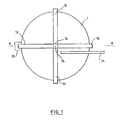
- Figure 1 is a schematic plan view of an apparatus of the invention including a wafer holder above a member containing a plurality of transducers.
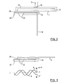
- Figure 2 is a cross sectional schematic illustration of the apparatus of Fig. 1 taken along line A-A showing a member containing a plurality of transducers and a planar surface of an object to be treated.
- Figure 3 is the cross section of the wafer and member of figure 2 with a corresponding plot of the megasonic wave front as a function of distance along the transducer-containing member.
- the invention generally encompasses the use of an apparatus containing a plurality of transducers arranged to transmit a progressive megasonic wave through a liquid containing a planar surface of an object.
- the method and apparatus of the invention can be used to provide improved megasonic cleaning and other improved processes involving the application of megasonic energy to liquids contacting a surface to be treated.
- the processes and apparatus of the invention are especially useful for cleaning wafers in the course of manufacturing integrated circuit chips.
- the apparatus of the invention is generally characterized by the presence of a plurality of transducers and one or more controllers for controlling the operation of the transducers such that one or more progressive megasonic waves is established in a liquid medium along a substantially planar surface of an object (typically a wafer to be cleaned or treated) by the operation transducers.
- the apparatus of the invention preferably comprises:
- Means for holding the object may be any object holder commonly used to hold the object to be treated.
- the object holder is suitable for holding a wafer such as semiconductor wafers commonly used in the manufacture of integrated circuit devices.
- the holder may be a simple vacuum chuck supported on a rotatable shaft such as described in U.S. Patents 4,326,553 and 4,064,885, the disclosures of which are incorporated herein by reference.
- the holder may be one which engages edges of the object such as disclosed in U.S. Patents 5,361,449 and 5,286,657, the disclosures of which are incorporated herein by reference.
- the holder engages simultaneously the edges of the object at at least three distinct points, more preferably at least four distinct points.
- the no set of three engaging points are colinear with each other.
- Edge-engaging holders are preferred where simultaneous treatment of two sides of a wafer is desired.
- Figures 1 and 2 show an embodiment of the invention where an edge-engaging holder is used.
- the holder has four gripping arms 10 with gripping edges 12 which grip a wafer 1.
- the arms are connected at an axis point 14.
- a shaft 16 for rotating the gripping arms (to thereby rotate a held wafer) is attached to the arms at axis point 14.
- Shaft 16 is preferably attached to a rotating means such as described in the above mentioned patents.
- the apparatus of the invention includes means for supplying a liquid whereby at least a portion of the liquid is brought into contact with the exposed planar surface of the object.
- the liquid supply means is preferably one or more pipes such as pipe 18 in Figure 2. At least one liquid supply means is located beneath the object wafer 1, such that it can supply liquid to contact the planar surface of object wafer 1 at a location on the planar surface that directly overlies a member 20 containing a series of megasonic transducers 22.
- the liquid supply means may further include a pressurized source (not shown) of the liquid to be used for treating the object surface.
- a further pipe 24 may be present over the object wafer 1 as shown in figure 1. Pipe 24 may be used to deliver liquid for simultaneous treatment of an additional surface of the wafer object 1.
- the liquid supply means made of a suitable material for delivery of neutral or acidic aqueous liquids. If desired, additional liquid pipes can be placed at desired locations about the object to provide additional supplies of liquid to a surface of the object.
- the apparatus of the invention contains a plurality of transducers 22 which are used to propagate a progressive megasonic wave in the liquid near the exposed planar surface of the object.
- the transducers are capable of operating at megasonic frequencies (0.8-6 MHz).
- the transducers are preferably oriented to have a direction of excursion or vibration substantially normal to the planar surface to be treated.
- the transducers are sufficiently proximate to each other and to the exposed planar surface to be treated such that a progressive megasonic wave can be propagated by the transducers in the liquid near the exposed surface.
- the plurality of transducers comprises at least three transducers which are colinear in a plane parallel with the exposed planar surface of the object. As shown in Fig.
- the transducers form a line extending from an interior region 26 of the planar surface toward an outer edge 28 of the planar surface.
- This radial orientation of the transducers allows for propagation a progressive megasonic wave radially outward from interior (preferably center) of the planar surface to be treated.
- sufficient transducers are radially oriented in this manner to create a progressive megasonic wave in the liquid from the center of the planar surface to an edge of the wafer or more preferably to beyond the edge of the wafer. In this way, the action of the progressive wave will be more uniform along the entire radial distance along the object surface.
- the transducers may be any conventional transducers commonly used in megasonic cleaning.
- the transducers are preferably housed in a housing member 30.
- the housing preferably has a flexible impermeable membrane which is coupled with the action of the transducers to transmit the energy of each of the plurality of transducers to the liquid supplied thereover.
- the membrane may be of any type commonly used to transfer megasonic energy to a liquid in conventional megasonic cleaning processes.
- the apparatus includes an electronic means for controlling the operating frequency of the transducers and a phase relationship of the transducers in a manner to create a progressive megasonic wave in the liquid near the exposed surface.
- the transducers are typically piezoelectric devices which are driven by an electric power source operating at the desired megasonic frequency. Preferably, all the transducers are operating at the same frequency. In some instances, it may be possible to vary the frequency of operation of subsets of transducers provided that the overall progressive wave is maintained. Operating the transducers at different phases is generally necessary to establish the progressive wave. An example of a phase relationship is shown in Fig. 3.
- the two curves, C and C' show the effective operation (sin q) of the transducers at two different times as a function of distance (r) along member 20.
- Points A and B in Fig. 3 represent effective transducer operation points that are 180° out of phase. It should be understood that the effect of each transducer extends to a certain region within the liquid. Thus, the progressive wave can correspond to the positioning of transducers located at other locations and spacings provided that the proper phase relationship is maintained.
- Electronic circuitry for creating the proper phase relationship in a series of transducers is described in U.S. Patent 4,768,256, the disclosure of which is incorporated herein by reference.
- the apparatus preferably further comprises means for moving the object in a plane parallel with the planar surface whereby different portions of the planar surface are contacted by the portion of the liquid carrying the propagated progressive megasonic wave.
- the means for moving said object preferably comprises a means for rotating said object in a plane parallel with the planar surface.
- the rotation preferably is about an axis which is normal to the planar surface, the rotation axis preferably passing through the center of the planar surface. Examples of suitable rotating means are disclosed in the above mentioned patents which describe various wafer holders.
- the megasonic transducer member 20 may rotated or moved relative to the object surface (e.g., as an alternative or supplement to moving the object), however, this is generally not preferred.
- the apparatus of the invention may include other expedients such as a collecting tank (not shown) for collecting liquid flowing over the megasonic cleaning member 20 or flowing off the object. Depending on the treatment operation being performed, it may be possible to reuse the liquid (with or without some form of remediation).
- the apparatus of the invention may include plural members 20, each containing a set of megasonic transducers operating to create a corresponding progressive megasonic wave. It should be understood that the various parts of the apparatus of the invention may be fixed in space and/or coupled to each other as appropriate to the intended function by attachment to the desired parts to each other or to other structures (e.g. chamber walls, support stands, etc.) as may be known in the art.
- the invention encompasses methods of contacting a substantially planar surface of an object with a liquid wherein a progressive megasonic wave is propagated through the liquid at the planar surface.
- the methods of the invention preferably comprise:
- the planar surface is preferably moved in a plane parallel with the planar surface whereby the liquid in the gap contacts a further portion of the substantially planar surface.
- the movement involves rotating the object about a center point in the planar surface (e.g., the center of a circular surface or a wafer).
- the megasonic energy is preferably maintained while the object is being rotated.
- the plurality of transducers preferably comprises at least three colinear transducers, the colinear transducers forming a line parallel with the substantially planar surface, the line extending from an interior portion of the planar surface toward an edge of the planar surface.
- the transducers are preferably operated at a frequency of about 0.8 - 6 MHz, more preferably about 1-2 MHz.
- the phase relationship of the transducers should be such that the progressive wave is maintained during operation of the transducers.
- the transducers are configured to propagate a progressive megasonic wave from the interior portion (e.g. center) of the planar surface to beyond the edge of the planar surface as shown in Fig. 1 and 2.
- the method of the invention may be used for any desired liquid contacting.
- the method of the invention comprises treatment of the object under conditions designed to clean or etch the object surface.
- Cleaning or etching processes may use liquids and treatment conditions (e.g., time, temperature) known in the art to be suitable for accomplishing these tasks with the objects of interest (typically wafers).
- the methods of the invention preferably involve the use of aqueous liquids.
- Such liquids may range from simply deionized water to liquids containing controlled amounts of gases, acids, bases, organic solvents, etc. as may be desired to accomplish cleaning and/or etching of the object surface.
- the action of the progressive megasonic wave may allow for relaxation of the treatment conditions used and/or improved treatment results for a given set of treatment conditions.
- the method may further include simultaneous treatment of a second surface (preferably substantially planar) of the object.
- the method would include contacting the second surface with a second liquid (identical or different from the liquid used in propagating the progressive megasonic wave).
Landscapes
- Cleaning Or Drying Semiconductors (AREA)
- Crystals, And After-Treatments Of Crystals (AREA)
- Cleaning By Liquid Or Steam (AREA)
Applications Claiming Priority (2)
| Application Number | Priority Date | Filing Date | Title |
|---|---|---|---|
| US189429 | 1998-11-10 | ||
| US09/189,429 US6021789A (en) | 1998-11-10 | 1998-11-10 | Wafer cleaning system with progressive megasonic wave |
Publications (3)
| Publication Number | Publication Date |
|---|---|
| EP1000673A2 true EP1000673A2 (de) | 2000-05-17 |
| EP1000673A3 EP1000673A3 (de) | 2000-09-20 |
| EP1000673B1 EP1000673B1 (de) | 2003-02-26 |
Family
ID=22697291
Family Applications (1)
| Application Number | Title | Priority Date | Filing Date |
|---|---|---|---|
| EP99307796A Expired - Lifetime EP1000673B1 (de) | 1998-11-10 | 1999-10-04 | System zum Reinigen von Halbleiterscheiben mit megasonischer Wanderwelle |
Country Status (5)
| Country | Link |
|---|---|
| US (1) | US6021789A (de) |
| EP (1) | EP1000673B1 (de) |
| JP (1) | JP2000150440A (de) |
| AT (1) | ATE233131T1 (de) |
| DE (1) | DE69905538T2 (de) |
Families Citing this family (26)
| Publication number | Priority date | Publication date | Assignee | Title |
|---|---|---|---|---|
| US6202658B1 (en) | 1998-11-11 | 2001-03-20 | Applied Materials, Inc. | Method and apparatus for cleaning the edge of a thin disc |
| DE10030718A1 (de) * | 2000-06-23 | 2002-01-10 | Univ Ilmenau Tech | Verfahren und Vorrichtung zum Reinigen von Gegenständen mit Schallwellen |
| US7451774B2 (en) * | 2000-06-26 | 2008-11-18 | Applied Materials, Inc. | Method and apparatus for wafer cleaning |
| AU2001270205A1 (en) * | 2000-06-26 | 2002-01-08 | Applied Materials, Inc. | Method and apparatus for wafer cleaning |
| US6763378B1 (en) * | 2000-10-12 | 2004-07-13 | International Business Machines Corporation | Synchronous TCP/IP port monitor for enhanced computer system security |
| US7105985B2 (en) * | 2001-04-23 | 2006-09-12 | Product Systems Incorporated | Megasonic transducer with focused energy resonator |
| US6928751B2 (en) * | 2001-06-12 | 2005-08-16 | Goldfinger Technologies, Llc | Megasonic cleaner and dryer system |
| US7100304B2 (en) * | 2001-06-12 | 2006-09-05 | Akrion Technologies, Inc. | Megasonic cleaner and dryer |
| US20030015494A1 (en) * | 2001-07-20 | 2003-01-23 | Seagate Technology Llc | Single layer resist lift-off process and apparatus for submicron structures |
| KR100927493B1 (ko) * | 2001-11-02 | 2009-11-17 | 프로덕트 시스템즈 인코포레이티드 | 방사출력 메가소닉 변환기 |
| US7185661B2 (en) * | 2002-05-06 | 2007-03-06 | Akrion Technologies, Inc. | Reciprocating megasonic probe |
| US6880560B2 (en) * | 2002-11-18 | 2005-04-19 | Techsonic | Substrate processing apparatus for processing substrates using dense phase gas and sonic waves |
| WO2004112093A2 (en) * | 2003-06-06 | 2004-12-23 | P.C.T. Systems, Inc. | Method and apparatus to process substrates with megasonic energy |
| AU2003903660A0 (en) * | 2003-07-16 | 2003-07-31 | Soniclean Pty Ltd | A space adaptable ultrasonic cleaning apparatus |
| NZ543157A (en) * | 2003-10-22 | 2008-09-26 | Soniclean Pty Ltd | An improved active wine barrel |
| WO2005039788A1 (en) * | 2003-10-22 | 2005-05-06 | Soniclean Pty Ltd | An apparatus and method for cleaning and recycling water used in cleaning of barrels |
| WO2006010997A1 (en) * | 2004-07-16 | 2006-02-02 | Darren Miles Bates | An apparatus and method of ultrasonic cleaning |
| US7418525B2 (en) * | 2004-10-29 | 2008-08-26 | International Business Machines Corporation | Shared simultaneously-connected removable drives and servers each housing an I/O controller which maintains an uninterrupted protocol connection |
| US7958899B2 (en) * | 2007-08-21 | 2011-06-14 | Dainippon Screen Mfg. Co., Ltd. | Substrate cleaning apparatus and substrate cleaning method |
| DE102007040851A1 (de) | 2007-08-29 | 2009-03-05 | Wacker Chemie Ag | Verfahren zum Reinigen von polykristallinem Silicium |
| US8051863B2 (en) * | 2007-10-18 | 2011-11-08 | Lam Research Corporation | Methods of and apparatus for correlating gap value to meniscus stability in processing of a wafer surface by a recipe-controlled meniscus |
| KR20120018296A (ko) * | 2009-03-31 | 2012-03-02 | 에이씨엠 리서치 (상하이) 인코포레이티드 | 반도체 웨이퍼 세정 방법 및 장치 |
| CN101927242B (zh) * | 2009-06-25 | 2014-08-20 | 盛美半导体设备(上海)有限公司 | 半导体硅片的清洗方法和装置 |
| US8539969B2 (en) * | 2010-07-30 | 2013-09-24 | Sematech, Inc. | Gigasonic brush for cleaning surfaces |
| EP2973560B1 (de) * | 2013-03-14 | 2019-03-13 | Koolance, Inc. | Reiniger für phonographenschallplatten |
| US10345211B2 (en) | 2016-03-28 | 2019-07-09 | Hemlock Semiconductor Operations Llc | Method of determining a concentration of a material not dissolved by silicon etchants contaminating a product |
Family Cites Families (21)
| Publication number | Priority date | Publication date | Assignee | Title |
|---|---|---|---|---|
| US2985003A (en) * | 1957-01-11 | 1961-05-23 | Gen Motors Corp | Sonic washer |
| US3117768A (en) * | 1960-11-21 | 1964-01-14 | Branson Instr | Ultrasonic transducers |
| US4064885A (en) * | 1976-10-26 | 1977-12-27 | Branson Ultrasonics Corporation | Apparatus for cleaning workpieces by ultrasonic energy |
| US4326553A (en) * | 1980-08-28 | 1982-04-27 | Rca Corporation | Megasonic jet cleaner apparatus |
| GB2097890B (en) * | 1981-05-01 | 1985-06-12 | Boulton Ltd William | Ultrasonic cleaning |
| FR2524909B1 (fr) * | 1982-04-08 | 1985-10-11 | Framatome Sa | Procede de degraissage de pieces au moyen d'ultra-sons et dispositif de mise en oeuvre de ce procede |
| JPS6116528A (ja) * | 1985-06-14 | 1986-01-24 | Hitachi Ltd | ウエハ洗浄装置 |
| US4768256A (en) * | 1986-11-07 | 1988-09-06 | Motoda Electronics Co., Ltd. | Ultrasonic wiper |
| US4869278A (en) * | 1987-04-29 | 1989-09-26 | Bran Mario E | Megasonic cleaning apparatus |
| JPH025538A (ja) * | 1988-06-24 | 1990-01-10 | Fujitsu Ltd | モールド金型及び樹脂封止型半導体装置の製造方法 |
| US4909266A (en) * | 1989-03-10 | 1990-03-20 | Frank Massa | Ultrasonic cleaning system |
| JPH04500033A (ja) * | 1989-05-17 | 1992-01-09 | ミンスキ ラディオテフニチェスキ インスティテュト | 液体媒体内の物品を超音波加工するための装置 |
| JPH0319337A (ja) * | 1989-06-16 | 1991-01-28 | Mitsubishi Electric Corp | ウエハ異物除去装置 |
| US5090432A (en) * | 1990-10-16 | 1992-02-25 | Verteq, Inc. | Single wafer megasonic semiconductor wafer processing system |
| JP2877216B2 (ja) * | 1992-10-02 | 1999-03-31 | 東京エレクトロン株式会社 | 洗浄装置 |
| US5383484A (en) * | 1993-07-16 | 1995-01-24 | Cfmt, Inc. | Static megasonic cleaning system for cleaning objects |
| US5368054A (en) * | 1993-12-17 | 1994-11-29 | International Business Machines Corporation | Ultrasonic jet semiconductor wafer cleaning apparatus |
| US5626913A (en) * | 1994-03-09 | 1997-05-06 | Tokyo Electron Limited | Resist processing method and apparatus |
| JP2830733B2 (ja) * | 1994-03-25 | 1998-12-02 | 日本電気株式会社 | 電解水生成方法および電解水生成機構 |
| US5601655A (en) * | 1995-02-14 | 1997-02-11 | Bok; Hendrik F. | Method of cleaning substrates |
| TW355815B (en) * | 1996-05-28 | 1999-04-11 | Canon Kasei Kk | Cleaning methods of porous surface and semiconductor surface |
-
1998
- 1998-11-10 US US09/189,429 patent/US6021789A/en not_active Expired - Fee Related
-
1999
- 1999-10-04 EP EP99307796A patent/EP1000673B1/de not_active Expired - Lifetime
- 1999-10-04 DE DE69905538T patent/DE69905538T2/de not_active Expired - Fee Related
- 1999-10-04 AT AT99307796T patent/ATE233131T1/de not_active IP Right Cessation
- 1999-10-13 JP JP11291234A patent/JP2000150440A/ja active Pending
Also Published As
| Publication number | Publication date |
|---|---|
| DE69905538T2 (de) | 2003-11-20 |
| DE69905538D1 (de) | 2003-04-03 |
| ATE233131T1 (de) | 2003-03-15 |
| JP2000150440A (ja) | 2000-05-30 |
| US6021789A (en) | 2000-02-08 |
| EP1000673A3 (de) | 2000-09-20 |
| EP1000673B1 (de) | 2003-02-26 |
Similar Documents
| Publication | Publication Date | Title |
|---|---|---|
| EP1000673B1 (de) | System zum Reinigen von Halbleiterscheiben mit megasonischer Wanderwelle | |
| US6821349B2 (en) | Method and apparatus for removing a liquid from a surface | |
| US9138861B2 (en) | CMP pad cleaning apparatus | |
| WO1999016109A1 (en) | Method and apparatus for removing a liquid from a surface | |
| KR20060024781A (ko) | 천공된 컨디셔닝 디스크를 이용한 진공 보조 패드 컨디셔닝시스템 및 방법 | |
| KR100468110B1 (ko) | 웨이퍼 처리 장치 | |
| KR20120018296A (ko) | 반도체 웨이퍼 세정 방법 및 장치 | |
| US20040025911A1 (en) | Apparatus for cleaning a semiconductor substrate by vibrating cleaning solution supplied onto the substrate | |
| US6805137B2 (en) | Method for removing contamination particles from substrates | |
| US20030037457A1 (en) | Particle removal apparatus | |
| US6779226B2 (en) | Factory interface particle removal platform | |
| US20070170812A1 (en) | System apparatus and methods for processing substrates using acoustic energy | |
| US7380560B2 (en) | Wafer cleaning apparatus with probe cleaning and methods of using the same | |
| CN101927242B (zh) | 半导体硅片的清洗方法和装置 | |
| US6766813B1 (en) | Apparatus and method for cleaning a wafer | |
| US6725564B2 (en) | Processing platform with integrated particle removal system | |
| JP5101813B2 (ja) | べベル処理装置 | |
| TWI823171B (zh) | 基板邊緣清潔和基板承載頭間隙清潔的設備和方法 | |
| JP2007005661A (ja) | ベベル研磨方法及びベベル研磨装置 | |
| JP3927936B2 (ja) | 枚葉式洗浄方法及び洗浄装置 | |
| EP1817791B1 (de) | Vorrichtung und verfahren zur nassbehandlung von wafern | |
| KR100927028B1 (ko) | 초음파 노즐 및 이를 포함하는 기판 세정 장치 | |
| KR100683275B1 (ko) | 진동 유닛 및 이를 포함하는 메가소닉 세정 장치 | |
| JP4187817B2 (ja) | 超音波洗浄装置 | |
| KR100927029B1 (ko) | 트랜스듀서 및 이를 포함하는 기판 세정 장치 |
Legal Events
| Date | Code | Title | Description |
|---|---|---|---|
| PUAI | Public reference made under article 153(3) epc to a published international application that has entered the european phase |
Free format text: ORIGINAL CODE: 0009012 |
|
| AK | Designated contracting states |
Kind code of ref document: A2 Designated state(s): AT BE CH CY DE DK ES FI FR GB GR IE IT LI LU MC NL PT SE |
|
| AX | Request for extension of the european patent |
Free format text: AL;LT;LV;MK;RO;SI |
|
| PUAL | Search report despatched |
Free format text: ORIGINAL CODE: 0009013 |
|
| AK | Designated contracting states |
Kind code of ref document: A3 Designated state(s): AT BE CH CY DE DK ES FI FR GB GR IE IT LI LU MC NL PT SE |
|
| AX | Request for extension of the european patent |
Free format text: AL;LT;LV;MK;RO;SI |
|
| 17P | Request for examination filed |
Effective date: 20010227 |
|
| AKX | Designation fees paid |
Free format text: AT BE CH CY DE DK ES FI FR GB GR IE IT LI LU MC NL PT SE |
|
| GRAG | Despatch of communication of intention to grant |
Free format text: ORIGINAL CODE: EPIDOS AGRA |
|
| 17Q | First examination report despatched |
Effective date: 20020514 |
|
| RAP1 | Party data changed (applicant data changed or rights of an application transferred) |
Owner name: KABUSHIKI KAISHA TOSHIBA Owner name: INTERNATIONAL BUSINESS MACHINES CORPORATION |
|
| GRAG | Despatch of communication of intention to grant |
Free format text: ORIGINAL CODE: EPIDOS AGRA |
|
| GRAG | Despatch of communication of intention to grant |
Free format text: ORIGINAL CODE: EPIDOS AGRA |
|
| GRAH | Despatch of communication of intention to grant a patent |
Free format text: ORIGINAL CODE: EPIDOS IGRA |
|
| GRAH | Despatch of communication of intention to grant a patent |
Free format text: ORIGINAL CODE: EPIDOS IGRA |
|
| GRAA | (expected) grant |
Free format text: ORIGINAL CODE: 0009210 |
|
| AK | Designated contracting states |
Designated state(s): AT BE CH CY DE DK ES FI FR GB GR IE IT LI LU MC NL PT SE |
|
| PG25 | Lapsed in a contracting state [announced via postgrant information from national office to epo] |
Ref country code: NL Free format text: LAPSE BECAUSE OF FAILURE TO SUBMIT A TRANSLATION OF THE DESCRIPTION OR TO PAY THE FEE WITHIN THE PRESCRIBED TIME-LIMIT Effective date: 20030226 Ref country code: LI Free format text: LAPSE BECAUSE OF FAILURE TO SUBMIT A TRANSLATION OF THE DESCRIPTION OR TO PAY THE FEE WITHIN THE PRESCRIBED TIME-LIMIT Effective date: 20030226 Ref country code: IT Free format text: LAPSE BECAUSE OF FAILURE TO SUBMIT A TRANSLATION OF THE DESCRIPTION OR TO PAY THE FEE WITHIN THE PRESCRIBED TIME-LIMIT;WARNING: LAPSES OF ITALIAN PATENTS WITH EFFECTIVE DATE BEFORE 2007 MAY HAVE OCCURRED AT ANY TIME BEFORE 2007. THE CORRECT EFFECTIVE DATE MAY BE DIFFERENT FROM THE ONE RECORDED. Effective date: 20030226 Ref country code: GR Free format text: LAPSE BECAUSE OF FAILURE TO SUBMIT A TRANSLATION OF THE DESCRIPTION OR TO PAY THE FEE WITHIN THE PRESCRIBED TIME-LIMIT Effective date: 20030226 Ref country code: FI Free format text: LAPSE BECAUSE OF FAILURE TO SUBMIT A TRANSLATION OF THE DESCRIPTION OR TO PAY THE FEE WITHIN THE PRESCRIBED TIME-LIMIT Effective date: 20030226 Ref country code: CH Free format text: LAPSE BECAUSE OF FAILURE TO SUBMIT A TRANSLATION OF THE DESCRIPTION OR TO PAY THE FEE WITHIN THE PRESCRIBED TIME-LIMIT Effective date: 20030226 Ref country code: BE Free format text: LAPSE BECAUSE OF FAILURE TO SUBMIT A TRANSLATION OF THE DESCRIPTION OR TO PAY THE FEE WITHIN THE PRESCRIBED TIME-LIMIT Effective date: 20030226 Ref country code: AT Free format text: LAPSE BECAUSE OF FAILURE TO SUBMIT A TRANSLATION OF THE DESCRIPTION OR TO PAY THE FEE WITHIN THE PRESCRIBED TIME-LIMIT Effective date: 20030226 |
|
| REG | Reference to a national code |
Ref country code: GB Ref legal event code: FG4D |
|
| REG | Reference to a national code |
Ref country code: CH Ref legal event code: EP |
|
| REG | Reference to a national code |
Ref country code: IE Ref legal event code: FG4D |
|
| REF | Corresponds to: |
Ref document number: 69905538 Country of ref document: DE Date of ref document: 20030403 Kind code of ref document: P |
|
| PG25 | Lapsed in a contracting state [announced via postgrant information from national office to epo] |
Ref country code: SE Free format text: LAPSE BECAUSE OF FAILURE TO SUBMIT A TRANSLATION OF THE DESCRIPTION OR TO PAY THE FEE WITHIN THE PRESCRIBED TIME-LIMIT Effective date: 20030526 Ref country code: PT Free format text: LAPSE BECAUSE OF FAILURE TO SUBMIT A TRANSLATION OF THE DESCRIPTION OR TO PAY THE FEE WITHIN THE PRESCRIBED TIME-LIMIT Effective date: 20030526 Ref country code: DK Free format text: LAPSE BECAUSE OF FAILURE TO SUBMIT A TRANSLATION OF THE DESCRIPTION OR TO PAY THE FEE WITHIN THE PRESCRIBED TIME-LIMIT Effective date: 20030526 |
|
| NLV1 | Nl: lapsed or annulled due to failure to fulfill the requirements of art. 29p and 29m of the patents act | ||
| PG25 | Lapsed in a contracting state [announced via postgrant information from national office to epo] |
Ref country code: ES Free format text: LAPSE BECAUSE OF FAILURE TO SUBMIT A TRANSLATION OF THE DESCRIPTION OR TO PAY THE FEE WITHIN THE PRESCRIBED TIME-LIMIT Effective date: 20030828 |
|
| ET | Fr: translation filed | ||
| PGFP | Annual fee paid to national office [announced via postgrant information from national office to epo] |
Ref country code: GB Payment date: 20031001 Year of fee payment: 5 |
|
| PG25 | Lapsed in a contracting state [announced via postgrant information from national office to epo] |
Ref country code: LU Free format text: LAPSE BECAUSE OF NON-PAYMENT OF DUE FEES Effective date: 20031004 Ref country code: CY Free format text: LAPSE BECAUSE OF FAILURE TO SUBMIT A TRANSLATION OF THE DESCRIPTION OR TO PAY THE FEE WITHIN THE PRESCRIBED TIME-LIMIT Effective date: 20031004 |
|
| PG25 | Lapsed in a contracting state [announced via postgrant information from national office to epo] |
Ref country code: IE Free format text: LAPSE BECAUSE OF NON-PAYMENT OF DUE FEES Effective date: 20031006 |
|
| PG25 | Lapsed in a contracting state [announced via postgrant information from national office to epo] |
Ref country code: MC Free format text: LAPSE BECAUSE OF NON-PAYMENT OF DUE FEES Effective date: 20031031 |
|
| PLBE | No opposition filed within time limit |
Free format text: ORIGINAL CODE: 0009261 |
|
| STAA | Information on the status of an ep patent application or granted ep patent |
Free format text: STATUS: NO OPPOSITION FILED WITHIN TIME LIMIT |
|
| 26N | No opposition filed |
Effective date: 20031127 |
|
| REG | Reference to a national code |
Ref country code: IE Ref legal event code: MM4A |
|
| PG25 | Lapsed in a contracting state [announced via postgrant information from national office to epo] |
Ref country code: GB Free format text: LAPSE BECAUSE OF NON-PAYMENT OF DUE FEES Effective date: 20041004 |
|
| PGFP | Annual fee paid to national office [announced via postgrant information from national office to epo] |
Ref country code: DE Payment date: 20041019 Year of fee payment: 6 |
|
| PGFP | Annual fee paid to national office [announced via postgrant information from national office to epo] |
Ref country code: FR Payment date: 20041021 Year of fee payment: 6 |
|
| GBPC | Gb: european patent ceased through non-payment of renewal fee |
Effective date: 20041004 |
|
| PG25 | Lapsed in a contracting state [announced via postgrant information from national office to epo] |
Ref country code: DE Free format text: LAPSE BECAUSE OF NON-PAYMENT OF DUE FEES Effective date: 20060503 |
|
| PG25 | Lapsed in a contracting state [announced via postgrant information from national office to epo] |
Ref country code: FR Free format text: LAPSE BECAUSE OF NON-PAYMENT OF DUE FEES Effective date: 20060630 |
|
| REG | Reference to a national code |
Ref country code: FR Ref legal event code: ST Effective date: 20060630 |