EP0992984A1 - Element mit magnetischem Tunneleffekt und Verfahren zur dessen Herstellung - Google Patents
Element mit magnetischem Tunneleffekt und Verfahren zur dessen Herstellung Download PDFInfo
- Publication number
- EP0992984A1 EP0992984A1 EP99118413A EP99118413A EP0992984A1 EP 0992984 A1 EP0992984 A1 EP 0992984A1 EP 99118413 A EP99118413 A EP 99118413A EP 99118413 A EP99118413 A EP 99118413A EP 0992984 A1 EP0992984 A1 EP 0992984A1
- Authority
- EP
- European Patent Office
- Prior art keywords
- magnetic
- layer
- tunnel barrier
- barrier layer
- metal layer
- Prior art date
- Legal status (The legal status is an assumption and is not a legal conclusion. Google has not performed a legal analysis and makes no representation as to the accuracy of the status listed.)
- Withdrawn
Links
Images

Classifications
-
- B—PERFORMING OPERATIONS; TRANSPORTING
- B82—NANOTECHNOLOGY
- B82Y—SPECIFIC USES OR APPLICATIONS OF NANOSTRUCTURES; MEASUREMENT OR ANALYSIS OF NANOSTRUCTURES; MANUFACTURE OR TREATMENT OF NANOSTRUCTURES
- B82Y25/00—Nanomagnetism, e.g. magnetoimpedance, anisotropic magnetoresistance, giant magnetoresistance or tunneling magnetoresistance
-
- G—PHYSICS
- G01—MEASURING; TESTING
- G01R—MEASURING ELECTRIC VARIABLES; MEASURING MAGNETIC VARIABLES
- G01R33/00—Arrangements or instruments for measuring magnetic variables
- G01R33/02—Measuring direction or magnitude of magnetic fields or magnetic flux
- G01R33/06—Measuring direction or magnitude of magnetic fields or magnetic flux using galvano-magnetic devices
- G01R33/09—Magnetoresistive devices
- G01R33/093—Magnetoresistive devices using multilayer structures, e.g. giant magnetoresistance sensors
-
- B—PERFORMING OPERATIONS; TRANSPORTING
- B82—NANOTECHNOLOGY
- B82Y—SPECIFIC USES OR APPLICATIONS OF NANOSTRUCTURES; MEASUREMENT OR ANALYSIS OF NANOSTRUCTURES; MANUFACTURE OR TREATMENT OF NANOSTRUCTURES
- B82Y10/00—Nanotechnology for information processing, storage or transmission, e.g. quantum computing or single electron logic
-
- B—PERFORMING OPERATIONS; TRANSPORTING
- B82—NANOTECHNOLOGY
- B82Y—SPECIFIC USES OR APPLICATIONS OF NANOSTRUCTURES; MEASUREMENT OR ANALYSIS OF NANOSTRUCTURES; MANUFACTURE OR TREATMENT OF NANOSTRUCTURES
- B82Y40/00—Manufacture or treatment of nanostructures
-
- G—PHYSICS
- G01—MEASURING; TESTING
- G01R—MEASURING ELECTRIC VARIABLES; MEASURING MAGNETIC VARIABLES
- G01R33/00—Arrangements or instruments for measuring magnetic variables
- G01R33/02—Measuring direction or magnitude of magnetic fields or magnetic flux
- G01R33/06—Measuring direction or magnitude of magnetic fields or magnetic flux using galvano-magnetic devices
- G01R33/09—Magnetoresistive devices
- G01R33/098—Magnetoresistive devices comprising tunnel junctions, e.g. tunnel magnetoresistance sensors
-
- G—PHYSICS
- G11—INFORMATION STORAGE
- G11B—INFORMATION STORAGE BASED ON RELATIVE MOVEMENT BETWEEN RECORD CARRIER AND TRANSDUCER
- G11B5/00—Recording by magnetisation or demagnetisation of a record carrier; Reproducing by magnetic means; Record carriers therefor
- G11B5/127—Structure or manufacture of heads, e.g. inductive
- G11B5/33—Structure or manufacture of flux-sensitive heads, i.e. for reproduction only; Combination of such heads with means for recording or erasing only
- G11B5/332—Structure or manufacture of flux-sensitive heads, i.e. for reproduction only; Combination of such heads with means for recording or erasing only using thin films
-
- G—PHYSICS
- G11—INFORMATION STORAGE
- G11B—INFORMATION STORAGE BASED ON RELATIVE MOVEMENT BETWEEN RECORD CARRIER AND TRANSDUCER
- G11B5/00—Recording by magnetisation or demagnetisation of a record carrier; Reproducing by magnetic means; Record carriers therefor
- G11B5/127—Structure or manufacture of heads, e.g. inductive
- G11B5/33—Structure or manufacture of flux-sensitive heads, i.e. for reproduction only; Combination of such heads with means for recording or erasing only
- G11B5/39—Structure or manufacture of flux-sensitive heads, i.e. for reproduction only; Combination of such heads with means for recording or erasing only using magneto-resistive devices or effects
- G11B5/3903—Structure or manufacture of flux-sensitive heads, i.e. for reproduction only; Combination of such heads with means for recording or erasing only using magneto-resistive devices or effects using magnetic thin film layers or their effects, the films being part of integrated structures
-
- H—ELECTRICITY
- H01—ELECTRIC ELEMENTS
- H01F—MAGNETS; INDUCTANCES; TRANSFORMERS; SELECTION OF MATERIALS FOR THEIR MAGNETIC PROPERTIES
- H01F10/00—Thin magnetic films, e.g. of one-domain structure
- H01F10/32—Spin-exchange-coupled multilayers, e.g. nanostructured superlattices
- H01F10/324—Exchange coupling of magnetic film pairs via a very thin non-magnetic spacer, e.g. by exchange with conduction electrons of the spacer
- H01F10/3254—Exchange coupling of magnetic film pairs via a very thin non-magnetic spacer, e.g. by exchange with conduction electrons of the spacer the spacer being semiconducting or insulating, e.g. for spin tunnel junction [STJ]
-
- H—ELECTRICITY
- H01—ELECTRIC ELEMENTS
- H01F—MAGNETS; INDUCTANCES; TRANSFORMERS; SELECTION OF MATERIALS FOR THEIR MAGNETIC PROPERTIES
- H01F41/00—Apparatus or processes specially adapted for manufacturing or assembling magnets, inductances or transformers; Apparatus or processes specially adapted for manufacturing materials characterised by their magnetic properties
- H01F41/14—Apparatus or processes specially adapted for manufacturing or assembling magnets, inductances or transformers; Apparatus or processes specially adapted for manufacturing materials characterised by their magnetic properties for applying magnetic films to substrates
- H01F41/30—Apparatus or processes specially adapted for manufacturing or assembling magnets, inductances or transformers; Apparatus or processes specially adapted for manufacturing materials characterised by their magnetic properties for applying magnetic films to substrates for applying nanostructures, e.g. by molecular beam epitaxy [MBE]
- H01F41/302—Apparatus or processes specially adapted for manufacturing or assembling magnets, inductances or transformers; Apparatus or processes specially adapted for manufacturing materials characterised by their magnetic properties for applying magnetic films to substrates for applying nanostructures, e.g. by molecular beam epitaxy [MBE] for applying spin-exchange-coupled multilayers, e.g. nanostructured superlattices
- H01F41/305—Apparatus or processes specially adapted for manufacturing or assembling magnets, inductances or transformers; Apparatus or processes specially adapted for manufacturing materials characterised by their magnetic properties for applying magnetic films to substrates for applying nanostructures, e.g. by molecular beam epitaxy [MBE] for applying spin-exchange-coupled multilayers, e.g. nanostructured superlattices applying the spacer or adjusting its interface, e.g. in order to enable particular effect different from exchange coupling
- H01F41/307—Apparatus or processes specially adapted for manufacturing or assembling magnets, inductances or transformers; Apparatus or processes specially adapted for manufacturing materials characterised by their magnetic properties for applying magnetic films to substrates for applying nanostructures, e.g. by molecular beam epitaxy [MBE] for applying spin-exchange-coupled multilayers, e.g. nanostructured superlattices applying the spacer or adjusting its interface, e.g. in order to enable particular effect different from exchange coupling insulating or semiconductive spacer
-
- H—ELECTRICITY
- H10—SEMICONDUCTOR DEVICES; ELECTRIC SOLID-STATE DEVICES NOT OTHERWISE PROVIDED FOR
- H10N—ELECTRIC SOLID-STATE DEVICES NOT OTHERWISE PROVIDED FOR
- H10N50/00—Galvanomagnetic devices
- H10N50/10—Magnetoresistive devices
-
- G—PHYSICS
- G11—INFORMATION STORAGE
- G11B—INFORMATION STORAGE BASED ON RELATIVE MOVEMENT BETWEEN RECORD CARRIER AND TRANSDUCER
- G11B5/00—Recording by magnetisation or demagnetisation of a record carrier; Reproducing by magnetic means; Record carriers therefor
- G11B5/127—Structure or manufacture of heads, e.g. inductive
- G11B5/33—Structure or manufacture of flux-sensitive heads, i.e. for reproduction only; Combination of such heads with means for recording or erasing only
- G11B5/39—Structure or manufacture of flux-sensitive heads, i.e. for reproduction only; Combination of such heads with means for recording or erasing only using magneto-resistive devices or effects
- G11B2005/3996—Structure or manufacture of flux-sensitive heads, i.e. for reproduction only; Combination of such heads with means for recording or erasing only using magneto-resistive devices or effects large or giant magnetoresistive effects [GMR], e.g. as generated in spin-valve [SV] devices
-
- Y—GENERAL TAGGING OF NEW TECHNOLOGICAL DEVELOPMENTS; GENERAL TAGGING OF CROSS-SECTIONAL TECHNOLOGIES SPANNING OVER SEVERAL SECTIONS OF THE IPC; TECHNICAL SUBJECTS COVERED BY FORMER USPC CROSS-REFERENCE ART COLLECTIONS [XRACs] AND DIGESTS
- Y10—TECHNICAL SUBJECTS COVERED BY FORMER USPC
- Y10S—TECHNICAL SUBJECTS COVERED BY FORMER USPC CROSS-REFERENCE ART COLLECTIONS [XRACs] AND DIGESTS
- Y10S428/00—Stock material or miscellaneous articles
- Y10S428/90—Magnetic feature
-
- Y—GENERAL TAGGING OF NEW TECHNOLOGICAL DEVELOPMENTS; GENERAL TAGGING OF CROSS-SECTIONAL TECHNOLOGIES SPANNING OVER SEVERAL SECTIONS OF THE IPC; TECHNICAL SUBJECTS COVERED BY FORMER USPC CROSS-REFERENCE ART COLLECTIONS [XRACs] AND DIGESTS
- Y10—TECHNICAL SUBJECTS COVERED BY FORMER USPC
- Y10T—TECHNICAL SUBJECTS COVERED BY FORMER US CLASSIFICATION
- Y10T428/00—Stock material or miscellaneous articles
- Y10T428/11—Magnetic recording head
- Y10T428/1107—Magnetoresistive
- Y10T428/1114—Magnetoresistive having tunnel junction effect
-
- Y—GENERAL TAGGING OF NEW TECHNOLOGICAL DEVELOPMENTS; GENERAL TAGGING OF CROSS-SECTIONAL TECHNOLOGIES SPANNING OVER SEVERAL SECTIONS OF THE IPC; TECHNICAL SUBJECTS COVERED BY FORMER USPC CROSS-REFERENCE ART COLLECTIONS [XRACs] AND DIGESTS
- Y10—TECHNICAL SUBJECTS COVERED BY FORMER USPC
- Y10T—TECHNICAL SUBJECTS COVERED BY FORMER US CLASSIFICATION
- Y10T428/00—Stock material or miscellaneous articles
- Y10T428/11—Magnetic recording head
- Y10T428/1193—Magnetic recording head with interlaminar component [e.g., adhesion layer, etc.]
Definitions
- This invention relates to a magnetic tunnelling element in which a pair of magnetic layers are laminated via a tunnel barrier layer and in which the tunnel current is caused to flow from one to the other magnetic layer, with the conductance of the tunnel current being changed in dependence upon the ratio of polarization of magnetization of the paired magnetic layers.
- This invention also relates to a method for manufacturing the magnetic tunnelling element.
- a magnetic tunnelling effect is displayed, in which the conductance of the tunnel current flowing in the insulating layer is changed in dependence upon the relative angle of magnetization of the paired magnetic metal layers. That is, a layered structure comprised of a thin insulating layer sandwiched between a pair of magnetic metal layers exhibits a magneto-resistance effect with respect to the tunnel current flowing in the insulating layer.
- the specific magnetoresistance can be theoretically calculated based on the ratio of polarization of magnetization of the paired magnetic metal layers.
- expectation may be made of the specific magnetoresistance amounting approximately to 40%.
- a magnetic tunnelling element having a layered structure comprised of a thin insulating layer sandwiched between paired magnetic metal layers is stirring up notice as an element for detecting an external magnetic field.
- a metal oxide is routinely used as the thin insulating layer.
- a metal oxide is used as an insulating layer, pinholes etc tend to be formed, such that shorting tends to be induced between the paired magnetic metal layers.
- the metal oxidation degree is insufficient, such that the tunnel barrier is incomplete such that the magnetic tunnelling effect is not displayed.
- the present invention provides a magnetic tunnelling element including a first magnetic layer, a tunnel barrier layer formed on the first magnetic layer; and a second magnetic layer formed on the tunnel barrier layer formed on the tunnel barrier layer, the tunnel current flowing between the first magnetic layer and the second magnetic layer via the tunnel barrier layer.
- the surface of the first magnetic layer carrying the tunnel barrier layer has a surface roughness (Ra) of 0.3 nm or less.
- the tunnel barrier layer 2 since the surface of the first magnetic metal layer carrying the tunnel barrier layer has an average surface roughness (Ra) of 0.3 nm or less, the tunnel barrier layer 2 has its surface planarized to a high degree, so that, with the present magnetic tunnelling element, the interface between the first magnetic metal layer and the tunnel barrier layer and that between the second magnetic metal layer and the tunnel barrier layer are in optimum states to display the magnetic tunnelling effect reliably.
- Ra average surface roughness
- the present invention provides a method for manufacturing a magnetic tunnelling element at least including a first magnetic metal layer, a tunnel barrier layer and a second magnetic metal layer, laminated together, in which the method includes the steps of forming the first magnetic layer so that its major surface will have an average roughness (Ra) of 0.3 nm or less, forming the tunnel barrier layer on the major surface of the first magnetic metal layer and forming the second magnetic metal layer on the tunnel barrier layer.
- Ra average roughness
- the tunnel barrier layer formed on this major surface can be of optimum surface properties. Therefore, with this technique, the first magnetic metal layer and the tunnel barrier layer can be formed to optimum states.
- the surface roughness (Ra) of the surface of the first magnetic metal layer carrying the tunnel barrier layer is 0.3 nm or less.
- the tunnel current is allowed to flow positively between the first magnetic metal layer and the second magnetic metal layer in the vicinity of the tunnel barrier layer. Therefore, the magnetic tunnelling element of the present invention positively exhibits the high magnetic tunnelling effect.
- the first magnetic metal layer is formed so that its major surface will have an average roughness (Ra) of 0.3 nm or less.
- Ra average roughness
- the magnetic tunnelling element can be provided which allows the current to flow reliably between the first magnetic metal layer and the second magnetic metal layer in the vicinity of the tunnel barrier layer. Therefore, with the present manufacturing method for the magnetic tunnelling element, a magnetic tunnelling element exhibiting a high magnetic tunnelling effect can be manufactured reliably.
- the present invention can be applied with advantage to a high output magnetic head.
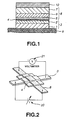
- a magnetic tunnelling element is made up of a first magnetic metal layer 3, having a NiFe layer 1 and a Co layer 2, a tunnel barrier layer 4 formed for overlying the first magnetic metal layer 3, and a second magnetic metal layer 8, having a Co layer 5, NiFe layer 6 and a FeMn layer 7.
- the magnetic tunnelling element is formed on a P-type Si substrate 9, on the surface of which has been formed an oxide layer approximately 300 nm in thickness by thermal oxidation.
- the present magnetic tunnelling element also has a Ta layer 9 on the FeMn layer 7 to prohibit corrosion of the FeMn layer 7. Meanwhile, this Ta layer is formed to a thickness of approximately 20 nm.
- the respective layers of the present magnetic tunnelling element were formed under sputtering conditions shown in Table 1. It is noted however that the magnetic tunnelling element and the manufacturing method therefor according to the present invention are not limitedtothese sputtering conditions.
- the tunnel barrier layer was formed by forming an Al layer and substantially oxidizing this Al film.
- the odidizing conditions are shown in the following Table 2.
- Ar gas flow rate 30 sccm oxygen gas flow rate (sccm) 15 sccm sputtering gas pressure 0.3 Pa discharging type RF back sputtering making power (W) 20W oxidation time (sec) 2000 sec
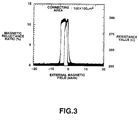
- the first magnetic metal layer 3 and the second magnetic metal layer 8, each in a strip shape, are formed for crossing each other, as shown in Fig.2.
- the tunnel barrier layer 4 are formed for covering at least the crossing region of the first magnetic metal layer 3 and the second magnetic metal layer 8.
- the vicinity of the end of the first magnetic metal layer 3 and the vicinity of the end of the second magnetic metal layer 8 are formed on the P-type Si substrate 9.
- an oxide layer is formed on the surface of the P-type Si substrate 9, there is no risk of shorting of the first magnetic metal layer 3 and the second magnetic metal layer 8.
- the NiFe layer 1 of the first magnetic metal layer 3 has been subjected to uniaxial orientation processing in a predetermined direction so that it proves a free magnetization film the direction of magnetization of which is changed by the external magnetic field.
- the NiFe layer 6 othe second magnetic metal layer 8 is exchange-coupled to the FeMn layer 7 so that it proves a fixed magnetization film having a fixed magnetization in a predetermined direction.
- the magnetization of the NiFe layer 1 is changed responsive to the external magnetic field.
- the magnetization of the NiFe layer 1 hasa predetermined angle with respect to that of the NiFe layer 7 of the second magnetic metal layer 8.
- a constant current source 20 is connected to an end of the first magnetic metal layer 3 and to an end of the magnetic metal layer 8, whist a voltmeter 21 is mounted on the other end of the first magnetic metal layer 3 and on the other end of the magnetic metal layer 8, as shown in Fig.2.
- the tunnel current which traverses the tunnel barrier layer flows between the first magnetic metal layer 3 and the magnetic metal layer 8, by a constant current furnished from the constant current source 20. If, in this magnetic tunnelling element, a predetermined external magnetic field is applied, the direction of magnetization of the NiFe layer 1 is at apredetermined angle with respect to that of the NiFe layer 7.
- the resistance value to the tunnel current is changed depending on the relative angle between the direction of magnetization of the NiFe layer 1 and that of the NiFe layer 7.
- the change in the resistance value to the tunnel current is represented as changes in voltage, so that, in the present magnetic tunnelling element, the external magnetic field can be detected by detecting voltage changes of the constant furnished current.
- the magnetic tunnelling element can be used for a variety of magnetic devices, such as, for example, a magnetic head, a magnetic sensor or a magnetic memory.
- the Co layer 2 of the first magnetic metal layer 3 and the Co layer 5 of the second magnetic metal layer 8 are higher in the ratio of spin polarization than the NiFe layer 1 or the NiFe layer 6 and hence serve for achieving a higher specific magnetoresistance. That is, by arranging the Co layer 2 and the Co layer 5 on an interface between the NiFe layer 1 and the tunnel barrier layer 4 and on an interface between the NiFe layer 6 and the tunnel barrier layer 4, it is possible to increase the specific magnetoresistance of the magnetic tunnelling element.
- the average roughness (Ra) of the major surface 3a of the first magnetic metal layer 3, stated differently, the surface of the Co layer 2, is set to 0.3 nm or less.
- the tunnel barrier layer 4 is formed on the Co layer 2 having the average roughness (Ra) not higher than 0.3 nm. Therefore, the tunnel barrier layer 4 has a substantially planar interface to the Co layer 2, while having a planar major surface.
- the second magnetic metal layer 8 is formed on the tunnel barrier layer 4, having a planar major surface, the interface between the tunnel barrier layer 4 and the second magnetic metal layer 8 is also planar.
- the direction of magnetization of the NiFe layer 1 makes a predetermined angle with that of the NiFe layer 7, depending on the external magnetic field, in the vicintiy of the interface to the tunnel barrier layer 4.
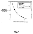
- the magnetic tunnelling effect is positively displayed in dependence upon the external magnetic field, as shown in Fig.3. It is noted that, in Fig.3, measurement was made in the external magnetic field of approximately ⁇ 24 kA/m (300 Oe). Also, as may be seen from Fig.3, the magnetic field of exchange coupling is 3.3 kA/m (approximately 41.25 Oe), with the resistance value and the specific magnetoresistance of the element being 25 ⁇ and approximately 15%, respectively.
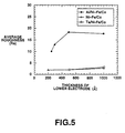
- the average roughness of the interface to the tunnel barrier layer that is the average roughness (Ra) of the Co layer
- the larger becomes the specific magnetoresistance and that, in order for the specific magnetoresistance to be not less than 5%, the average roughness (Ra) of the Co layer needs to be 0.03 nm or less.
- the average roughness (Ra) of the Co layer could be set to 0.15 nm, thus achieving a specific magnetoresistance as high as 18%.
- Fig.5 The measured results are shown in Fig.5, from which it isseen that, if the Al underlying layer is provided for the first magnetic metal layer 3, the average roughness is increased with increase in the thickness of the Al underlying layer. Conversely, if there is no underlying layer or if there is the Ta underlying layer, the average roughness is scarcely changed with changes in thickness.
- the average roughness of the first magnetic metal layer 3 can be decreased by reducing the thickness of the Al layer.
- the thickness of the Al underlying layer By decresingthe thickness of the Al underlying layer to decrease the average roughness of the first magnetic metal layer 3, it is possible to increase the specific magnetoresistance of the magnetic tunnelling element.
- the specific magnetoresistance tends to disappear with increased thickness of the Al underlying layer. If there is no underlying layer or if there is the Ta underlying layer, a predetermined specific magnetoresistance is displayed regardless of the overall thickness. It is seen from this that, in the presence of the Al underlying layer, the magnetic tunnelling element shows predetermined changes in the magnetoresistance by reducing the thickness of the Al layer.
Landscapes
- Engineering & Computer Science (AREA)
- Chemical & Material Sciences (AREA)
- Nanotechnology (AREA)
- Physics & Mathematics (AREA)
- Crystallography & Structural Chemistry (AREA)
- Manufacturing & Machinery (AREA)
- General Physics & Mathematics (AREA)
- Condensed Matter Physics & Semiconductors (AREA)
- Power Engineering (AREA)
- Spectroscopy & Molecular Physics (AREA)
- Mathematical Physics (AREA)
- Theoretical Computer Science (AREA)
- Hall/Mr Elements (AREA)
- Magnetic Heads (AREA)
Applications Claiming Priority (2)
| Application Number | Priority Date | Filing Date | Title |
|---|---|---|---|
| JP10263696A JP2000099923A (ja) | 1998-09-17 | 1998-09-17 | 磁気トンネル素子及びその製造方法 |
| JP26369698 | 1998-09-17 |
Publications (1)
| Publication Number | Publication Date |
|---|---|
| EP0992984A1 true EP0992984A1 (de) | 2000-04-12 |
Family
ID=17393075
Family Applications (1)
| Application Number | Title | Priority Date | Filing Date |
|---|---|---|---|
| EP99118413A Withdrawn EP0992984A1 (de) | 1998-09-17 | 1999-09-16 | Element mit magnetischem Tunneleffekt und Verfahren zur dessen Herstellung |
Country Status (3)
| Country | Link |
|---|---|
| US (1) | US6312840B1 (de) |
| EP (1) | EP0992984A1 (de) |
| JP (1) | JP2000099923A (de) |
Cited By (6)
| Publication number | Priority date | Publication date | Assignee | Title |
|---|---|---|---|---|
| WO2002029911A3 (en) * | 2000-10-02 | 2002-06-20 | Motorola Inc | Tunelling magnetoresistance (tmr) material having ultra-thin magnetic layer |
| US6956763B2 (en) | 2003-06-27 | 2005-10-18 | Freescale Semiconductor, Inc. | MRAM element and methods for writing the MRAM element |
| US6967366B2 (en) | 2003-08-25 | 2005-11-22 | Freescale Semiconductor, Inc. | Magnetoresistive random access memory with reduced switching field variation |
| US7129098B2 (en) | 2004-11-24 | 2006-10-31 | Freescale Semiconductor, Inc. | Reduced power magnetoresistive random access memory elements |
| US7184300B2 (en) | 2001-10-16 | 2007-02-27 | Freescale Semiconductor, Inc. | Magneto resistance random access memory element |
| US7465589B2 (en) | 2002-07-17 | 2008-12-16 | Everspin Technologies, Inc. | Multi-state magnetoresistance random access cell with improved memory storage density |
Families Citing this family (11)
| Publication number | Priority date | Publication date | Assignee | Title |
|---|---|---|---|---|
| JP3593652B2 (ja) * | 2000-03-03 | 2004-11-24 | 富士通株式会社 | 磁気ランダムアクセスメモリ装置 |
| TWI222630B (en) * | 2001-04-24 | 2004-10-21 | Matsushita Electric Industrial Co Ltd | Magnetoresistive element and magnetoresistive memory device using the same |
| JP2003086866A (ja) * | 2001-09-13 | 2003-03-20 | Anelva Corp | スピンバルブ型巨大磁気抵抗薄膜の製造方法 |
| US7248446B2 (en) * | 2001-11-27 | 2007-07-24 | Seagate Technology Llc | Magnetoresistive element using an organic nonmagnetic layer |
| US6638774B2 (en) * | 2002-01-15 | 2003-10-28 | Infineon Technologies, Ag | Method of making resistive memory elements with reduced roughness |
| JP2003283000A (ja) * | 2002-03-27 | 2003-10-03 | Toshiba Corp | 磁気抵抗効果素子およびこれを有する磁気メモリ |
| WO2003092084A1 (en) * | 2002-04-23 | 2003-11-06 | Matsushita Electric Industrial Co., Ltd. | Magnetoresistive element, manufacturing method thereof, magnetic head, magnetic memory, and magnetic recording device using the same |
| KR100612884B1 (ko) * | 2004-12-30 | 2006-08-14 | 삼성전자주식회사 | 자기 논리 소자와 그 제조 및 동작 방법 |
| JP2009055050A (ja) * | 2008-10-06 | 2009-03-12 | Canon Anelva Corp | スピンバルブ型巨大磁気抵抗薄膜またはtmr膜の製造方法 |
| JP2009158089A (ja) * | 2009-04-06 | 2009-07-16 | Canon Anelva Corp | スピンバルブ型巨大磁気抵抗薄膜またはtmr膜の製造方法 |
| KR101708548B1 (ko) * | 2015-02-06 | 2017-02-22 | 한양대학교 산학협력단 | 개선된 터널 배리어 구조를 갖는 mtj 셀 및 그 제작 방법 |
Citations (2)
| Publication number | Priority date | Publication date | Assignee | Title |
|---|---|---|---|---|
| US5764567A (en) * | 1996-11-27 | 1998-06-09 | International Business Machines Corporation | Magnetic tunnel junction device with nonferromagnetic interface layer for improved magnetic field response |
| EP0898315A1 (de) * | 1997-08-18 | 1999-02-24 | Hitachi, Ltd. | Magnetowiderstandelement mit Tunneleffekt und dieses element benützende Sensor |
-
1998
- 1998-09-17 JP JP10263696A patent/JP2000099923A/ja not_active Abandoned
-
1999
- 1999-09-16 EP EP99118413A patent/EP0992984A1/de not_active Withdrawn
- 1999-09-16 US US09/397,069 patent/US6312840B1/en not_active Expired - Fee Related
Patent Citations (2)
| Publication number | Priority date | Publication date | Assignee | Title |
|---|---|---|---|---|
| US5764567A (en) * | 1996-11-27 | 1998-06-09 | International Business Machines Corporation | Magnetic tunnel junction device with nonferromagnetic interface layer for improved magnetic field response |
| EP0898315A1 (de) * | 1997-08-18 | 1999-02-24 | Hitachi, Ltd. | Magnetowiderstandelement mit Tunneleffekt und dieses element benützende Sensor |
Non-Patent Citations (3)
| Title |
|---|
| B.G. PARK AND T.D.LEE: "Dependence of tunneling magnetoresistance on CoFe interfacial layer thickness in NiFe/Al2O3/NiFe tunnel junctions", IEEE TRANSACTIONS ON MAGNETICS, vol. 35, no. 5, September 1999 (1999-09-01), usa, pages 2919 - 2921, XP002128404 * |
| INDO Y ET AL: "Influence of interlayer roughness on magnetoresistive effect of ferromagnetic tunneling junctions", JOURNAL OF MAGNETISM AND MAGNETIC MATERIALS, vol. 198, June 1999 (1999-06-01), Netherlands, pages 155 - 157, XP000874195 * |
| MOODERA J S ET AL: "FERROMAGNETIC-INSULATOR-FERROMAGNETIC TUNNELING: SPIN-DEPENDENT TUNNELING AND LARGE MAGNETORESISTANCE IN TRILAYER JUNCTIONS (INVITED)", JOURNAL OF APPLIED PHYSICS,US,AMERICAN INSTITUTE OF PHYSICS. NEW YORK, vol. 79, no. 8, PART 02A, 15 April 1996 (1996-04-15), pages 4724-4729, XP000695592, ISSN: 0021-8979 * |
Cited By (7)
| Publication number | Priority date | Publication date | Assignee | Title |
|---|---|---|---|---|
| WO2002029911A3 (en) * | 2000-10-02 | 2002-06-20 | Motorola Inc | Tunelling magnetoresistance (tmr) material having ultra-thin magnetic layer |
| CN100375309C (zh) * | 2000-10-02 | 2008-03-12 | 自由度半导体公司 | 具有超薄磁性层的tmr材料 |
| US7184300B2 (en) | 2001-10-16 | 2007-02-27 | Freescale Semiconductor, Inc. | Magneto resistance random access memory element |
| US7465589B2 (en) | 2002-07-17 | 2008-12-16 | Everspin Technologies, Inc. | Multi-state magnetoresistance random access cell with improved memory storage density |
| US6956763B2 (en) | 2003-06-27 | 2005-10-18 | Freescale Semiconductor, Inc. | MRAM element and methods for writing the MRAM element |
| US6967366B2 (en) | 2003-08-25 | 2005-11-22 | Freescale Semiconductor, Inc. | Magnetoresistive random access memory with reduced switching field variation |
| US7129098B2 (en) | 2004-11-24 | 2006-10-31 | Freescale Semiconductor, Inc. | Reduced power magnetoresistive random access memory elements |
Also Published As
| Publication number | Publication date |
|---|---|
| US6312840B1 (en) | 2001-11-06 |
| JP2000099923A (ja) | 2000-04-07 |
Similar Documents
| Publication | Publication Date | Title |
|---|---|---|
| EP0992984A1 (de) | Element mit magnetischem Tunneleffekt und Verfahren zur dessen Herstellung | |
| US7163755B2 (en) | Magneto-resistive element | |
| KR100462926B1 (ko) | 스핀터널 자기저항효과막과 소자 및 이를 사용한 자기저항센서 및 자기 장치와 그 제조방법 | |
| KR100344030B1 (ko) | 자기 소자, 자기 메모리 디바이스, 자기저항 효과 헤드 및 자기 저장 시스템. | |
| KR100347084B1 (ko) | 외부자계센서로서 이용 가능한 자기터널접합소자 | |
| US6335081B1 (en) | Tunnel magnetoresistance effect element | |
| JP3331397B2 (ja) | トンネル磁気抵抗効果素子 | |
| US7280323B2 (en) | Magnetoresistance effect element and magnetic head | |
| EP0814519B1 (de) | Element mit magnetoresistivem Effekt, sein Herstellungsverfahren und Magnetkopf daraus | |
| JPH06181349A (ja) | 磁気抵抗効果型弱磁界センサ | |
| US6621666B2 (en) | Magnetoresistive-effect element having electrode layers oppositely disposed on main surfaces of a magnetoresistive-effect thin film having hard magnetic bias layers with a particular resistivity | |
| US6519123B1 (en) | Method to manufacture magnetic tunneling elements using inductively coupled plasma | |
| US11320498B2 (en) | Magnetic-field-applying bias film, and magnetic detection element and magnetic detector including the same | |
| KR100306312B1 (ko) | 자기저항효과소자 | |
| US7535683B2 (en) | Magnetoresistive head with improved in-stack longitudinal biasing layers | |
| US7068479B2 (en) | Magnetoresistance effect element comprising nano-contact portion not more than a fermi length, and magnetic head utilizing same | |
| KR100269989B1 (ko) | 스핀 밸브형 박막소자 및 그 제조방법 | |
| US20080247097A1 (en) | Magnetoresistance effect element and magnetic head | |
| US20050105221A1 (en) | Magnetoresistive-effect thin film, magnetoresistive-effect element, and magnetoresistive-effect magnetic head | |
| WO2019035294A1 (ja) | 交換結合膜ならびにこれを用いた磁気抵抗効果素子および磁気検出装置 | |
| KR20010043167A (ko) | 자기 센서와 그 제조 방법, 강자성 터널 접합 소자와 그제조 방법, 및 이들을 사용한 자기 헤드 | |
| JP2001052315A (ja) | スピンバルブ型薄膜磁気素子及び薄膜磁気ヘッド及びスピンバルブ型薄膜磁気素子の製造方法 | |
| US6287709B1 (en) | Spin-valve film, magnetoresistance-effect device and magnetoresistance-effect magnetic head | |
| JP3151133B2 (ja) | 磁気抵抗効果型ヘッド | |
| US20030129454A1 (en) | Spin valve magnetoresistive sensor |
Legal Events
| Date | Code | Title | Description |
|---|---|---|---|
| PUAI | Public reference made under article 153(3) epc to a published international application that has entered the european phase |
Free format text: ORIGINAL CODE: 0009012 |
|
| AK | Designated contracting states |
Kind code of ref document: A1 Designated state(s): DE FR GB |
|
| AX | Request for extension of the european patent |
Free format text: AL;LT;LV;MK;RO;SI |
|
| 17P | Request for examination filed |
Effective date: 20000919 |
|
| AKX | Designation fees paid |
Free format text: DE FR GB |
|
| STAA | Information on the status of an ep patent application or granted ep patent |
Free format text: STATUS: THE APPLICATION HAS BEEN WITHDRAWN |
|
| 18W | Application withdrawn |
Withdrawal date: 20020215 |