EP0985196B9 - Capteur dactyloscopique presentant des caracteristiques de commande de gain et procedes associes - Google Patents
Capteur dactyloscopique presentant des caracteristiques de commande de gain et procedes associes Download PDFInfo
- Publication number
- EP0985196B9 EP0985196B9 EP98921014A EP98921014A EP0985196B9 EP 0985196 B9 EP0985196 B9 EP 0985196B9 EP 98921014 A EP98921014 A EP 98921014A EP 98921014 A EP98921014 A EP 98921014A EP 0985196 B9 EP0985196 B9 EP 0985196B9
- Authority
- EP
- European Patent Office
- Prior art keywords
- electric field
- reference voltage
- range
- converter
- field sensing
- Prior art date
- Legal status (The legal status is an assumption and is not a legal conclusion. Google has not performed a legal analysis and makes no representation as to the accuracy of the status listed.)
- Expired - Lifetime
Links
Images


Classifications
-
- G—PHYSICS
- G06—COMPUTING OR CALCULATING; COUNTING
- G06V—IMAGE OR VIDEO RECOGNITION OR UNDERSTANDING
- G06V40/00—Recognition of biometric, human-related or animal-related patterns in image or video data
- G06V40/10—Human or animal bodies, e.g. vehicle occupants or pedestrians; Body parts, e.g. hands
- G06V40/12—Fingerprints or palmprints
- G06V40/13—Sensors therefor
- G06V40/1306—Sensors therefor non-optical, e.g. ultrasonic or capacitive sensing
-
- G—PHYSICS
- G07—CHECKING-DEVICES
- G07C—TIME OR ATTENDANCE REGISTERS; REGISTERING OR INDICATING THE WORKING OF MACHINES; GENERATING RANDOM NUMBERS; VOTING OR LOTTERY APPARATUS; ARRANGEMENTS, SYSTEMS OR APPARATUS FOR CHECKING NOT PROVIDED FOR ELSEWHERE
- G07C9/00—Individual registration on entry or exit
- G07C9/30—Individual registration on entry or exit not involving the use of a pass
- G07C9/32—Individual registration on entry or exit not involving the use of a pass in combination with an identity check
- G07C9/37—Individual registration on entry or exit not involving the use of a pass in combination with an identity check using biometric data, e.g. fingerprints, iris scans or voice recognition
Definitions
- the present invention relates to the field of personal identification and verification, and, more particularly, to the field of fingerprint sensing and processing.
- Fingerprint sensing and matching is a reliable and widely used technique for personal identification or verification.
- a common approach to fingerprint identification involves scanning a sample fingerprint or an image thereof and storing the image and/or unique characteristics of the fingerprint image. The characteristics of a sample fingerprint may be compared to information for reference fingerprints already in a database to determine proper identification of a person, such as for verification purposes.
- a typical electronic fingerprint sensor is based upon illuminating the finger surface using visible light, infrared light, or ultrasonic radiation. The reflected energy is captured with some form of camera, for example, and the resulting image is framed, digitized and stored as a static digital image.
- the specification of US-A-4,210,899 discloses an optical scanning fingerprint reader cooperating with a central processing station for a secure access application, such as admitting a person to a location or providing access to a computer terminal.
- the specification of US-A-4,525,859 discloses a video camera for capturing a fingerprint image and uses the minutiae of the fingerprints, that is, the branches and endings of the fingerprint ridges, to determine a match with a database of reference fingerprints.
- WO 86/06527 discloses a skin pattern recognition device in which an image of the print of a skin pattern is projected onto a photo-detector device and the intensity variations of the print image in at least one region thereof is digitally processed to form a digital signal which is compared to a second signal derived from stored skin pattern information.
- optical sensing may be affected by stained fingers or an optical sensor may be deceived by presentation of a photograph or printed image of a fingerprint rather than a true live fingerprint.
- optical schemes may require relatively large spacings between the finger contact surface and associated imaging components.
- such sensors typically require precise alignment and complex scanning of optical beams.
- US-A-4,353,056 discloses another approach to sensing a live fingerprint.
- it discloses an array of extremely small capacitors located in a plane parallel to the sensing surface of the device.
- a voltage distribution in a series connection of the capacitors may change.
- the voltages on each of the capacitors is determined by multiplexor techniques.
- US-A-5,325,442 discloses a fingerprint sensor including a plurality of sensing electrodes. Active addressing of the sensing electrodes is made possible by the provision of a switching device associated with each sensing electrode. A capacitor is effectively formed by each sensing electrode in combination with the respective overlying portion of the finger surface which, in turn, is at ground potential.
- the sensor is fabricated using semiconductor wafer and integrated circuit technology.
- the dielectric material upon which the finger is placed may be provided by silicon nitride or a polyimide which may be provided as a continuous layer over an array of sensing electrodes.
- JP-A-01146464 discloses an AGC circuit in a picture reader in which an analogue signal from a reader sensor is converted into a digital signal so as to apply digital processing and facilitate the setting of the AGC characteristic and eliminate dispersion of an AGC output.
- JP-A-02031377 discloses an automatic level controller for sound recording and reproducing device in which the number of ports is reduced by using a Digital to Analogue converter to generate a reference voltage for an AD converter and automatically controlling the range of the AD converter.
- EP 0 786 745 A2 published on 30 July 1997 and claiming a priority date of 26 January 1996 discloses an enhanced security fingerprint sensor package having A/D converters for converting analogue signals from an array of electric field sensing elements.
- a reference voltage of the A/D converters is under control of a processor so as to achieve a limited degree of dynamic contrast compensation.
- An object of the present invention is to provide a fingerprint sensor and related methods so that the fingerprint sensor may accommodate variations in image signal intensities, such as between different fingers, for different sensing conditions, or based on manufacturing process variations, for example.
- the present invention consists in a fingerprint sensor comprising an array of fingerprint sensing elements, at least one analogue-to-digital (A/D) converter for converting an analogue signal from at least one fingerprint sensing element to a digital signal based upon at least one reference voltage for controlling the range of the A/D converter, the or each A/D converter having at least one reference voltage input for receiving the reference voltage, scanning means for operating said at least one AID converter and said array of fingerprint sensing elements to perform sequential A/D conversions of predetermined ones of said array of fingerprint sensing elements, and reference voltage determining and setting means for controlling the at least one reference voltage of the or each A/D converter based upon prior A/D conversions to thereby provide enhanced conversion resolution, said reference voltage determining and setting means comprising a processor including histogram generating means for generating a histogram based upon prior A/D conversions.
- A/D analogue-to-digital
- the present invention consists in a method for operating a fingerprint sensor of a type comprising an array of fingerprint sensing elements, the method comprising the steps of, converting analogue signals from the array of fingerprint sensing elements to digital signals using at least one A/D converter having a controllable range, performing sequential A/D conversions of predetermined ones of the array of fingerprint sensing elements, and determining and controlling the range of the at least one A/D converter based upon prior A/D conversions to thereby provide enhanced conversion resolution, in which the range of the at least one A/D converter is controllable based upon at least one reference voltage, and the step of determining and controlling the range comprises controlling the at least one reference voltage, wherein the step of converting analogue signals comprises converting same using at least one amplifier having a controllable gain for permitting setting of the range, and the step of determining and controlling the range comprises controlling the range using the amplifier, generating a histogram based upon a prior A/D conversions, and setting a default range for initial ones of the
- the conversion resolution is enhanced despite variations in sensed fingers, conditions, or despite process variations resulting from manufacturing.
- the A/D conversion means preferably comprises a plurality or bank of A/D converters for simultaneously converting analogue signals from a corresponding plurality of fingerprint sensing elements.
- the range determining and setting means may include at least one digital-to-analogue converter connected between the processor and the at least one reference voltage input.
- the AID converters may typically include a first reference voltage input and a second reference voltage input for setting corresponding first and second range points thereby defining the range.
- the A/D conversion means may include at least one amplifier having a controllable gain for permitting setting of the range.
- the range determining and setting means may comprise default setting means for setting a default range for initial ones of the fingerprint sensing elements.
- Each of the fingerprint sensing elements may be provided by an electric field sensing electrode and an amplifier associated therewith.
- a shield electrode may also be associated with each electric field sensing electrode and be connected to a respective amplifier.
- FIGS. 1-3 depict the fingerprint sensor 30 that includes a housing or package 51, a dielectric layer 52 exposed on an upper surface of the package which provides a placement surface for the finger, and a plurality of output pins, not shown.
- a first conductive strip or external electrode 54 around the periphery of the dielectric layer 52 , and a second external electrode 53 provide contact electrodes for the finger 79 .
- the sensor 30 provides output signals in a range of sophistication levels depending on the level of processing.
- the sensor 30 includes a plurality of individual pixels or sensing elements 30a arranged in array pattern as perhaps best shown in FIG. 3 . These sensing elements are relatively small so as to be capable of sensing the ridges 59 and intervening valleys 60 of a typical fingerprint. Live fingerprint readings, as from the electric field sensor 30 , is less reliable than optical sensing, because the impedance of the skin of a finger in a pattern of ridges and valleys is extremely difficult to simulate. In contrast, an optical sensor may be deceived by a readily deceived by a photograph or other similar image of a fingerprint, for example.
- the sensor 30 includes a substrate 65 , and one or more active semiconductor devices formed thereon, such as the schematically illustrated amplifier 73.
- a first metal layer 66 interconnects the active semiconductor devices.
- a second or ground plane electrode layer 68 is above the first metal layer 66 and separated therefrom by an insulating layer 67 .
- a third metal layer 71 is positioned over another dielectric layer 70 .
- the first external electrode 54 is connected to an excitation drive amplifier 74 which, in turn, drives the finger 79 with a signal which may be typically in the range of about 1 KHz to 1 MHz.
- the drive or excitation electronics are thus relatively uncomplicated and the overall cost of the sensor 30 may be relatively low, while the reliability is great.
- a circularly shaped electric field sensing electrode 78 is on the insulating layer 70 .
- the sensing electrode 78 may be connected to sensing integrated electronics, such as amplifier 73 formed adjacent the substrate 65 as schematically illustrated.
- An annularly shaped shield electrode 80 surrounds the sensing electrode 78 in spaced relation therefrom.
- the sensing electrode 78 and its surrounding shield electrode 80 may have other shapes, such as hexagonal, for example, to facilitate a close packed arrangement or array of pixels or sensing elements 30a .
- the shield electrode 80 is an active shield which is driven by a portion of the output of the amplifier 73 to help focus the electric field energy and, moreover, to thereby reduce the need to drive adjacent electric field sensing electrodes 78 .
- the sensor 30 includes only three metal or electrically conductive layers 66,68 , and 71 .
- the sensor 30 can be made without requiring additional metal layers which would otherwise increase the manufacturing cost, and, perhaps, reduce yields. Accordingly, the sensor 30 is less expensive and may be more rugged and reliable than a sensor including four or more metal layers.
- the amplifier 73 is operated at a gain of greater than about one to drive the shield electrode 80 . Stability problems do not adversely affect the operation of the amplifier 73 . Moreover, the common mode and general noise rejection are greatly enhanced. In addition, operating at again greater than one tends to focus the electric field with respect co the sensing electrode 78 .
- the sensing elements 30a operate at very low currants and at very high impedances.
- the output signal from each sensing electrode 78 is desirably about 5 to 10 millivolts to reduce the effects of noise and permit further processing of the signals.
- the approximate diameter of each sensing element 30a as defined by the outer dimensions of the shield electrode 80 , may be about 50.8 to 127 ⁇ m in diameter.
- the ground plane electrode 68 protects the active electronic devices from unwanted excitation.
- the various signal feed through conductors for the electrodes 78,80 to the active electronic circuitry may be readily formed.
- the overall contact or sensing surface for the sensor 30 may desirably be about 12.7 by 12.7 mm - a size which may be readily manufactured and still provide a sufficiently large surface for accurate fingerprint sensing and identification.
- the sensor 30 in accordance with the invention is also fairly tolerant of dead pixels or sensing elements 30a .
- a typical sensor 30 includes an array of about 256 by 256 pixels or sensor elements, although other array sizes are also contemplated by the present invention.
- the sensor 30 may also be fabricated at one time using primarily conventional semiconductor manufacturing techniques to thereby significantly reduce the manufacturing costs.
- FIG. 4 shows another aspect of the sensor 30 .
- the sensor may include power control means for controlling operation of active circuit portions 100 based upon sensing finger contact with the first external electrode 54 as determined by the finger sense block or circuit 101 .
- the finger sense circuit 101 may operate based upon a change in impedance to an oscillator to thereby determine finger contact.
- the power control means may include wake-up means for only powering active circuit portions upon sensing finger contact with the first external electrode to conserve power.
- the power control means may further comprise protection means for grounding active circuit portions upon not sensing finger contact with the first external electrode. A combination of wake-up and protection controller circuits 101 are illustrated.
- the fingerprint sensor 30 further comprise finger charge bleed means for bleeding a charge from a finger or other object upon contact therewith.
- the finger charge bleed means may be provided by the second external electrode 53 carried by the package 51 for contact by a finger, and a charge bleed resistor 104 connected between the second external electrode and an earth ground.
- the second electrode may alternately be provided by a movable electrically conductive cover 53' slidably connected to the package 51 for covering the opening to the exposed upper dielectric layer 52 .
- a pivotally connected cover is also contemplated by the present invention. Accordingly, under normal conditions, the charge would be bled from the finger as the cover 53' is moved to expose the sensing portion of the sensor 30 .
- the finger charge bleed means and power control means may be such that the active portions remain grounded until the charge bleed means can remove the charge on the finger before powering the active circuit portions, such as by providing a brief delay during wake-up sufficient to permit the charge to be discharged through the resistor 104 . Accordingly, power may be conserved in the sensor 30 and BSD protection provided by the sensor so that the sensor is relatively inexpensive, yet robust and conserves power.
- FIG. 5 refers to another feature of the sensor 30 .
- the dielectric covering 52 comprise a z-axis anisotropic dielectric layer 110 for focusing an electric field, shown by the illustrated field lines, at each of the electric field sensing electrodes 78 .
- the z-axis anisotropic dielectric layer 110 of the present invention may have a thickness in range of about 2.54 to 101.6 ⁇ m.
- the z-axis anisotropic dielectric layer 110 is also preferably chemically resistant and mechanically strong to withstand contact with fingers, and co permit periodic cleanings with solvents.
- the z-axis anisotropic dielectric layer 110 may preferably define an outermost protective surface for the integrated circuit die 120 .
- the overall dielectric covering 52 may further include at least one relatively thin oxide, nitride, carbide, or diamond layer 111 on the integrated circuit die 120 and beneath the z-axis anisotropic dielectric layer 110 .
- the thin layer 111 will typically be relatively hard, and the z-axis anisotropic dielectric layer 110 is desirably softer to thereby absorb more mechanical activity.
- the 2-axis anisotropic dielectric layer 110 may be provided by a plurality of oriented dielectric particles in a cured matrix.
- the z-axis anisotropic dielectric layer 110 may comprise barium titanate in a polyimide matrix.
- FIG. 6 shows another variation of a z-axis dielectric cover 52' by a plurality of high dielectric portions 112 aligned with corresponding electric field sensing electrodes 78 , and a surrounding matrix of lower dielectric portions 113 .
- This embodiment of the dielectric covering 52' may be formed in a number of ways, such as by forming a layer of either the high dielectric or low dielectric portions, selectively etching same, and filling the openings with the opposite material.
- Another approach may be to use polarizable microcapsules and subjecting same to an electric field during curing of a matrix material. A material may be compressed to cause the z-axis anisotropy.
- the third metal layer 71 (FIG. 2) preferably further includes a plurality of capacitive coupling pads 116a-118a for permitting capacitive coupling of the integrated circuit die 120.
- the dielectric covering 52 is preferably continuous over the capacitive coupling pads 116a-118a and the array of electric field sensing electrodes 78 of the pixels 30a (FIG. 1).
- it is conventional to create openings through an outer coating to electrically connect to the bond pads. Unfortunately, these openings would provide pathways for water and/or other contaminants to come in contact with and damage the die.
- a portion of the package 51 includes a printed circuit board 122 which carries corresponding pads 115b-118b.
- a power modulation circuit 124 is coupled to pads 115b-116b
- a signal modulation circuit 126 is illustrated coupled to pads 117b-118b. Both power and signals may be coupled between the printed circuit board 122 and the integrated circuit die 120 , further using the illustrated power demodulation/regulator circuit 127 , and the signal demodulation circuit 128 .
- the z-axis anisotropic dielectric layer 110 also advantageously reduces cross-talk between adjacent capacitive coupling pads.
- This embodiment of the invention 30 presents no penetrations through the dielectric covering 52 for moisture to enter and damage the integrated circuit die 120 .
- another level of insulation is provided between the integrated circuit and the external environment.
- the package 51 has an opening aligned with the array of electric field sensing electrodes 78 (FIGS. 1-3 ).
- the capacitive coupling and z-axis anisotropic layer 110 may be advantageously used in a number of applications in addition to the illustrated fingerprint sensor 30 , and particularly where it is desired to have a continuous film covering the upper surface of the integrated circuit die 120 and pads 116a-118a .
- the fingerprint sensor 30 may be considered as comprising an array of fingerprint sensing elements 130 and associated active circuits 131 for generating signals relating to the fingerprint image.
- the sensor 30 also includes an impedance matrix 135 connected to the active circuits for filtering the signals therefrom.
- the impedance matrix 135 includes a plurality of impedance elements 136 with a respective impedance element connectable between each active circuit of a respective fingerprint sensing element as indicated by the central node 138 , and the other active circuits (outer nodes 140 ).
- the impedance matrix 135 also includes a plurality of switches 137 with a respective switch connected in series with each impedance element 136.
- An input signal may be supplied to the central node 138 via the illustrated switch 142 and its associated impedance element 143.
- the impedance element may one or more of a resistor as illustrated, and a capacitor 134.
- Filter control means may operate the switches 137 to perform processing of the signals generated by the active circuits 131.
- the fingerprint sensing elements 130 may be electric field sensing electrodes 78, and the active circuits 131 may be amplifiers 73 (FIG. 2).
- Ridge flow determining means 145 may be provided for selectively operating the switches 137 of the matrix 135 to determine ridge flow directions of the fingerprint image. More particularly, the ridge flow determining means 145 may selectively operate the switches 137 for determining signal strength vectors relating to ridge flow directions of the fingerprint image.
- the sensor 30 may include core location determining means 146 cooperating with the ridge flow determining means 145 for determining a core location of the fingerprint image.
- the position of the core is helpful, for example, in extracting and processing minutiae from the fingerprint image.
- a binarizing filter 150 is provided for selectively operating the switches 137 to convert a gray scale fingerprint image to a binarized fingerprint image.
- the impedance matrix 135 may be used to provide dynamic image contrast enhancement.
- an edge smoothing filter 155 may be readily implemented to improve the image.
- other spatial filters 152 may also be implemented using the impedance matrix 135 for selectively operating the switches 137 to spatially filter the fingerprint image. Accordingly, processing of the fingerprint image may be carried out at the sensor 30 and thereby reduce additional downstream computational requirements.
- FIG. 9 shows the impedance matrix 135 that comprise a plurality of impedance elements with a respective impedance element 136 connectable between each active circuit for a given fingerprint sensing element 130 and eight other active circuits for respective adjacent fingerprint sensing elements.
- the control means 153 is for sequentially powering sets of active circuits 131 to conserve power.
- the respective impedance elements 136 are desirably also sequentially connected to perform the filtering function.
- the powered active circuits 131 may be considered as defining a cloud or kernel.
- the power control means 153 may be operated in an adaptive fashion whereby the size of the area used for filtering is dynamically changed for preferred image characteristics.
- the power control means 153 may also power only certain ones of the active circuits corresponding to a predetermined area of the array of sensing elements 130.
- Reader control means 154 may be provided to read only predetermined subsets of each set of active circuits 131 so that a contribution from adjacent active circuits is used for filtering. In other words, only a subset of active circuits 131 are typically simultaneously read although adjacent active circuits 131 and associated impedance elements 136 are also powered and connected, respectively. For example, 16 impedance elements 136 could define a subset and be readily simultaneously read. The subset size could be optimized for different sized features to be determined.
- the array of sense elements 130 can be quickly read, and power consumption substantially reduced since all of the active circuits 131 need not be powered for reading a given set of active circuits.
- the combination of the power control and impedance matrix features described herein may permit power savings by a factor of about 10 as compared to powering the full array.
- Another advantage of the fingerprint sensor 30 is to guard against spoofing or deception of the sensor into incorrectly treating a simulated image as a live fingerprint image.
- optical sensors may be deceived or spoofed by using a paper with a fingerprint image thereon.
- the electric field sensing of the fingerprint sensor 30 provides an effective approach to avoiding spoofing based upon the complex impedance of a finger.
- the fingerprint sensor 30 may be considered as including an array of impedance sensing elements 160 for generating signals related to a finger 79 or other object positioned adjacent thereto.
- the impedance sensing elements 160 are provided by electric field sensing electrodes 78 and amplifiers 73 (FIG. 2) associated therewith.
- a guard shield 80 may be associated with each electric field sensing electrode 78 and connected to a respective amplifier 73.
- Spoof reducing means 161 is provided for determining whether or not an impedance of the object positioned adjacent the array of impedance sensing elements 160 corresponds to a live finger 79 to thereby reduce spoofing of the fingerprint sensor by an object other than a live finger.
- a spoofing may be indicated, such as by the schematically illustrated lamp 163 and/or used to block further processing.
- a live fingerprint determination may also be indicated by a lamp 164 and/or used to permit further processing of the fingerprint image.
- the spoof reducing means 161 may include impedance determining means 165 to detect a complex impedance having a phase angle in a range of about 10 to 60 degrees corresponding to a live finger 79 .
- the spoof reducing means 161 may detect an impedance having a phase angle of about 0 degrees corresponding to some objects other than a live finger, such as a sheet of paper having an image thereon, for example.
- the spoof reducing means 161 may detect an impedance of 90 degrees corresponding to other objects.
- the fingerprint sensor 30 includes drive means for driving the array of impedance sensing elements 160 , such as the illustrated excitation amplifier 74 (FIG. 2).
- the sensor also includes synchronous demodulator means 170 for synchronously demodulating signals from the array of impedance sensing elements 160 .
- the spoof reducing means comprises means for operating the synchronous demodulator means 170 at at least one predetermined phase rotation angle.
- the synchronous demodulator means 170 could be operated in a range of about 10 to 60 degrees, and the magnitude compared to a predetermined threshold indicative of a live fingerprint.
- a live fingerprint typically has a complex impedance within the range of 10 to 60 degrees.
- ratio generating and comparing means 172 may be provided for cooperating with the synchronous demodulator means 170 for synchronously demodulating signals at first and second phase angles ⁇ 1 , ⁇ 2 , generating an amplitude ratio thereof, and comparing the amplitude ratio to a predetermined threshold to determine whether the object is a live fingerprint or other object.
- the synchronous demodulator 170 may be readily used to generate the impedance information desired for reducing spoofing of the sensor 30 by an object other than a live finger.
- the first angle ⁇ 1 and the second ⁇ 2 may have a difference in a range of about 45 to 90 degrees, for example.
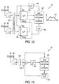
- the fingerprint sensor 30 also includes an automatic gain control feature to account for a difference in intensity of the image signals generated by different fingers or under different conditions, and also to account for differences in sensor caused by process variations. It is important for accurately producing a fingerprint image, that the sensor can discriminate between the ridges and valleys of the fingerprint. Accordingly, the sensor 30 includes a gain control feature, a first embodiment of which is understood with reference to FIG. 12.
- the portion of the fingerprint sensor 30 includes an array of fingerprint sensing elements in the form of the electric field sensing electrodes 78 and surrounding shield electrodes 80 connected to the amplifiers 73.
- Other fingerprint sensing elements may also benefit from the following automatic gain control implementations.
- the signal processing circuitry of the sensor 30 includes a plurality of analog-to-digital (A/D) converters 180 as illustrated. Moreover, each of these A/D converters 180 may have a controllable scale. Scanning means 182 sequentially connects different elements to the bank of A/D converters 180.
- the illustrated gain processor 185 provides range determining and setting means for controlling the range of the A/D converters 180 based upon prior A/D conversions to thereby provide enhanced conversion resolution.
- the A/D converters 180 may comprise the illustrated reference voltage input V ref and offset voltage input V offset for permitting setting of the range.
- the range determining and setting means may also comprise a first digital-to-analog D/A converter 186 connected between the gain processor 185 and the reference voltage V ref inputs of the A/D converters 180.
- a second D/A converter 189 is also illustratively connected to the offset voltage inputs V offset from the gain processor 185.
- the gain processor 185 may comprise histogram generating means for generating a histogram, as described above, and based upon prior A/D conversions.
- the graph adjacent the gain processor 185 in FIG. 12 illustrates a typical histogram plot 191 .
- the histogram plot 191 includes two peaks corresponding to the sensed ridges and valleys of the fingerprint. By setting the range for the A/D converters 180 , the peaks can be readily positioned as desired to thereby account for the variations and use the full resolution of the A/D converters 180.
- the A/D converters 180 may include an associated input amplifier for permitting setting of the range.
- the range determining and setting means may also comprise the illustrated gain processor 185 , and wherein the amplifier is a programmable gain amplifier (PGA) 187 connected to the processor.
- PGA programmable gain amplifier
- a digital word output from the gain processor 185 sets the gain of the PGA 187 so that full use of the resolution of the A/D converters 180 is obtained for best accuracy.
- a second digital word output from the gain processor 185 and coupled to the amplifier 187 through the illustrated D/A converter 192 may also control the offset of the amplifier.
- the range determining and setting means of the gain processor 185 may comprise default setting means for setting a default range for initial ones of the fingerprint sensing elements.
- the automatic gain control feature allows the D/A converters 180 to operate over their full resolution range to thereby increase the accuracy of the image signal processing.
- a fingerprint sensor includes an array of fingerprint sensing elements; analog-to-digital (A/D) converters having a controllable range; a scanner to perform sequential A/D conversions of predetermined ones of the array of fingerprint sensing elements; and a range determining and setting circuit for controlling the range of the A/D converters based upon prior A/D conversions to thereby provide enhanced conversion resolution.
- a plurality of A/D converters are used for simultaneously converting analog signals from a corresponding plurality of fingerprint sensing elements.
- the A/D converters may include at least one reference voltage input for permitting setting of first and second points of the range.
- the range scale determining and setting circuit generate a histogram based upon prior A/D conversions.
Landscapes
- Engineering & Computer Science (AREA)
- Human Computer Interaction (AREA)
- Physics & Mathematics (AREA)
- General Physics & Mathematics (AREA)
- Multimedia (AREA)
- Theoretical Computer Science (AREA)
- Image Input (AREA)
- Measurement Of Length, Angles, Or The Like Using Electric Or Magnetic Means (AREA)
- Measurement Of The Respiration, Hearing Ability, Form, And Blood Characteristics Of Living Organisms (AREA)
Claims (6)
- Détecteur d'empreintes digitales (30), comprenant un substrat (65), une matrice d'éléments détecteurs d'un champ électrique (78, 130), au moins un convertisseur (180) analogique/numérique (A/N) permettant de convertir un signal analogique provenant d'au moins un élément détecteur d'un champ électrique (78, 130) en un signal numérique fondé sur au moins une tension de référence afin de commander la plage du convertisseur A/N (180), le (ou chaque) convertisseur A/N (180) ayant au moins une entrée de tension de référence afin de recevoir la tension de référence, un moyen formant scanner (182) permettant de faire fonctionner ledit au moins un convertisseur A/N et ladite matrice d'éléments détecteurs d'un champ électrique (78, 130) afin d'effectuer des conversions A/N séquentielles des signaux analogiques provenant d'éléments détecteurs prédéterminés parmi la matrice d'éléments détecteurs d'un champ électrique, et des moyens de détermination et de fixation d'une tension de référence (185) permettant de commander ladite au moins une tension de référence du (de chaque) convertisseur A/N (180) en se fondant sur les conversions A/N précédentes, afin de fournir ainsi une résolution de conversion améliorée, lesdits moyens de détermination et de fixation d'une tension de référence comprenant un processeur (185) incluant un moyen générateur d'histogramme afin de générer un histogramme fondé sur les conversions A/N précédentes.
- Détecteur d'empreintes digitales selon la revendication 1, dans lequel lesdits moyens de détermination et de fixation d'une tension de référence comprennent en outre au moins un convertisseur numérique-analogique (186) connecté entre ledit processeur (185) et ladite au moins une entrée de tension de référence.
- Détecteur d'empreintes digitales selon la revendication 1, dans lequel ledit au moins un convertisseur A/N comprend au moins un amplificateur (187) permettant de fixer la plage.
- Détecteur d'empreintes digitales selon la revendication 1, 2 ou 3, dans lequel ledit au moins un convertisseur A/N (180) comprend une pluralité de convertisseurs A/N (180) permettant de convertir, simultanément, des signaux analogiques provenant d'une pluralité correspondante d'éléments détecteurs d'un champ électrique (78, 130).
- Détecteur d'empreintes digitales selon l'une quelconque des revendications précédentes, dans lequel lesdits moyens de détermination et de fixation d'une tension de référence comprennent des moyens de fixation par défaut, afin de fixer au moins une tension de référence par défaut pour les éléments initiaux parmi lesdits éléments détecteurs d'un champ électrique, chacun desdits éléments détecteurs d'un champ électrique comprenant une électrode de détection d'un champ électrique (78) et un amplificateur (73) associé à celle-ci, et comprenant en outre une électrode blindée (80) associée à chacune des électrodes de détection d'un champ électrique (78) et connectée à un amplificateur respectif (73).
- Procédé de fonctionnement d'un détecteur d'empreintes digitales (30) d'un type comprenant une matrice d'éléments détecteurs d'un champ électrique (78, 130), ce procédé comprenant les étapes de :dans lequel l'étape de conversion des signaux analogiques comprend la conversion de ceux-ci en utilisant au moins un amplificateur (187) ayant un gain pouvant être commandé, afin de permettre la commande de la plage en utilisant l'amplificateur (187), la génération d'un histogramme en se fondant sur les conversions A/N précédentes, et la fixation d'une plage par défaut pour les éléments initiaux parmi les éléments détecteurs d'un champ électrique (78, 130).conversion des signaux analogiques provenant de la matrice d'éléments détecteurs d'un champ électrique (78, 130) en signaux numériques en utilisant au moins un convertisseur A/N (180) ayant une plage pouvant être commandée,réalisation de conversions séquentielles A/N de signaux analogiques provenant d'éléments prédéterminés parmi la matrice d'éléments détecteurs d'un champ électrique (78, 130), etdétermination et commande de la plage dudit au moins un convertisseur A/N (180) en se fondant sur les conversions A/N précédentes afin de fournir une résolution de conversion améliorée, dans laquelle la plage dudit au moins un convertisseur A/N (180) peut être commandée en se fondant sur au moins une tension de référence, et l'étape de détermination et de commande de la plage comprend la commande de ladite au moins une tension de référence,
Applications Claiming Priority (3)
| Application Number | Priority Date | Filing Date | Title |
|---|---|---|---|
| US858142 | 1997-05-16 | ||
| US08/858,142 US6259804B1 (en) | 1997-05-16 | 1997-05-16 | Fingerprint sensor with gain control features and associated methods |
| PCT/US1998/009292 WO1998052157A1 (fr) | 1997-05-16 | 1998-05-06 | Capteur dactyloscopique presentant des caracteristiques de commande de gain et procedes associes |
Publications (3)
| Publication Number | Publication Date |
|---|---|
| EP0985196A1 EP0985196A1 (fr) | 2000-03-15 |
| EP0985196B1 EP0985196B1 (fr) | 2002-12-04 |
| EP0985196B9 true EP0985196B9 (fr) | 2003-05-02 |
Family
ID=25327595
Family Applications (1)
| Application Number | Title | Priority Date | Filing Date |
|---|---|---|---|
| EP98921014A Expired - Lifetime EP0985196B9 (fr) | 1997-05-16 | 1998-05-06 | Capteur dactyloscopique presentant des caracteristiques de commande de gain et procedes associes |
Country Status (8)
| Country | Link |
|---|---|
| US (1) | US6259804B1 (fr) |
| EP (1) | EP0985196B9 (fr) |
| JP (1) | JP4129892B2 (fr) |
| KR (1) | KR20010012635A (fr) |
| CN (1) | CN1290383A (fr) |
| AU (1) | AU7371598A (fr) |
| DE (1) | DE69809907T2 (fr) |
| WO (1) | WO1998052157A1 (fr) |
Families Citing this family (95)
| Publication number | Priority date | Publication date | Assignee | Title |
|---|---|---|---|---|
| EP1038259B1 (fr) * | 1997-12-18 | 2003-04-09 | Infineon Technologies AG | Dispositif d'enregistrement d'images |
| CA2323891A1 (fr) * | 1998-03-12 | 1999-09-16 | Peter Lauster | Cran d'arret pour arme a feu portative |
| JP2000172833A (ja) * | 1998-12-10 | 2000-06-23 | Omron Corp | 指紋照合装置 |
| DE19901384A1 (de) | 1999-01-15 | 2000-07-27 | Siemens Ag | Elektronisches Bauelement und Verwendung einer darin enthaltenen Schutzstruktur |
| US6674993B1 (en) * | 1999-04-30 | 2004-01-06 | Microvision, Inc. | Method and system for identifying data locations associated with real world observations |
| JP2001005951A (ja) * | 1999-06-24 | 2001-01-12 | Nec Shizuoka Ltd | 指紋読み取り装置における静電気除去方法、指紋読み取り装置及び指紋読み取り装置を備えた端末装置 |
| JP3679953B2 (ja) * | 1999-09-14 | 2005-08-03 | 富士通株式会社 | 生体情報を用いた個人認証システム |
| EP1146471B1 (fr) * | 2000-04-14 | 2005-11-23 | Infineon Technologies AG | Capteur biométrique capacitif |
| US6518560B1 (en) * | 2000-04-27 | 2003-02-11 | Veridicom, Inc. | Automatic gain amplifier for biometric sensor device |
| DE60125097T8 (de) * | 2000-06-08 | 2007-10-31 | Nippon Telegraph And Telephone Corp. | Kapatizitives Sensorgerät zur Erkennung kleiner Muster |
| NO314647B1 (no) * | 2000-06-09 | 2003-04-22 | Idex Asa | Målesystem for fingeravtrykksensor |
| NO315017B1 (no) * | 2000-06-09 | 2003-06-23 | Idex Asa | Sensorbrikke, s¶rlig for måling av strukturer i en fingeroverflate |
| NO315016B1 (no) * | 2000-06-09 | 2003-06-23 | Idex Asa | Miniatyrisert sensor |
| US7565541B1 (en) * | 2000-06-21 | 2009-07-21 | Microvision, Inc. | Digital fingerprint identification system |
| US6665428B1 (en) * | 2000-08-28 | 2003-12-16 | Stmicroelectronics, Inc. | Resistive finger detection for fingerprint sensor |
| US6990219B2 (en) * | 2000-12-15 | 2006-01-24 | Nippon Telegraph And Telephone Corporation | Image capturing method and apparatus and fingerprint collation method and apparatus |
| DE10110724A1 (de) * | 2001-03-06 | 2002-09-26 | Infineon Technologies Ag | Fingerabdrucksensor mit Potentialmodulation des ESD-Schutzgitters |
| WO2002089038A2 (fr) | 2001-04-27 | 2002-11-07 | Atrua Technologies, Inc. | Systeme de capteur capacitif a sensibilite de mesure de capacitance amelioree |
| US7259573B2 (en) * | 2001-05-22 | 2007-08-21 | Atrua Technologies, Inc. | Surface capacitance sensor system using buried stimulus electrode |
| EP1407477A4 (fr) * | 2001-05-22 | 2006-06-07 | Atrua Technologies Inc | Ensemble de connexion ameliore pour capteurs de circuit integre |
| JP2003287587A (ja) * | 2002-03-27 | 2003-10-10 | Toshiba Corp | プラント保護計装装置 |
| US7006078B2 (en) * | 2002-05-07 | 2006-02-28 | Mcquint, Inc. | Apparatus and method for sensing the degree and touch strength of a human body on a sensor |
| US6891490B2 (en) * | 2002-06-05 | 2005-05-10 | Slicex, Inc. | Analog-to-digital converter with digital signal processing functionality to emulate many different sample frequencies, resolutions, and architectures |
| US6856778B2 (en) * | 2002-08-15 | 2005-02-15 | Hewlett-Packard Development Company, L.P. | System and method for recycling hydrocarbon-based carrier liquid |
| FR2849244B1 (fr) * | 2002-12-20 | 2006-03-10 | Sagem | Procede de determination du caractere vivant d'un element porteur d'une empreinte digitale |
| US7474772B2 (en) * | 2003-06-25 | 2009-01-06 | Atrua Technologies, Inc. | System and method for a miniature user input device |
| US7587072B2 (en) * | 2003-08-22 | 2009-09-08 | Authentec, Inc. | System for and method of generating rotational inputs |
| US7280677B2 (en) * | 2003-10-10 | 2007-10-09 | Authentec, Inc. | Electronic device including fingerprint sensor and display having selectable menu items and associated methods |
| DE10356147A1 (de) * | 2003-12-02 | 2005-06-30 | Giesecke & Devrient Gmbh | Digitalisierung einer Papillarstruktur |
| US7697729B2 (en) * | 2004-01-29 | 2010-04-13 | Authentec, Inc. | System for and method of finger initiated actions |
| WO2005079413A2 (fr) * | 2004-02-12 | 2005-09-01 | Atrua Technologies, Inc. | Systeme et procede d'emulation d'operations avec la souris utilisant des capteurs d'images avec les doigts |
| GB2412775A (en) * | 2004-03-31 | 2005-10-05 | Seiko Epson Corp | Fingerprint scanner and method of auto focusing one |
| US7280679B2 (en) * | 2004-10-08 | 2007-10-09 | Atrua Technologies, Inc. | System for and method of determining pressure on a finger sensor |
| KR20060038274A (ko) * | 2004-10-29 | 2006-05-03 | 엘지전자 주식회사 | 지문 인식 센서 및 이를 이용한 이동 통신 단말기의 지문인식 장치 |
| AU2005302945B2 (en) * | 2004-11-15 | 2012-07-19 | Nec Corporation | Living body feature innput device |
| US20060103633A1 (en) * | 2004-11-17 | 2006-05-18 | Atrua Technologies, Inc. | Customizable touch input module for an electronic device |
| US20060181521A1 (en) * | 2005-02-14 | 2006-08-17 | Atrua Technologies, Inc. | Systems for dynamically illuminating touch sensors |
| CA2598482C (fr) * | 2005-02-17 | 2012-04-17 | Authentec, Inc. | Appareil a capteur de doigt utilisant le reechantillonnage des images et procedes correspondants |
| US7831070B1 (en) | 2005-02-18 | 2010-11-09 | Authentec, Inc. | Dynamic finger detection mechanism for a fingerprint sensor |
| US8231056B2 (en) * | 2005-04-08 | 2012-07-31 | Authentec, Inc. | System for and method of protecting an integrated circuit from over currents |
| US7505613B2 (en) * | 2005-07-12 | 2009-03-17 | Atrua Technologies, Inc. | System for and method of securing fingerprint biometric systems against fake-finger spoofing |
| US8358816B2 (en) * | 2005-10-18 | 2013-01-22 | Authentec, Inc. | Thinned finger sensor and associated methods |
| EP1949299A1 (fr) * | 2005-10-18 | 2008-07-30 | Authentec, Inc. | Capteur d'empreinte digitale comprenant un circuit souple, et methodes associees |
| US7940249B2 (en) * | 2005-11-01 | 2011-05-10 | Authentec, Inc. | Devices using a metal layer with an array of vias to reduce degradation |
| US7868874B2 (en) | 2005-11-15 | 2011-01-11 | Synaptics Incorporated | Methods and systems for detecting a position-based attribute of an object using digital codes |
| JP4182988B2 (ja) * | 2006-04-28 | 2008-11-19 | 日本電気株式会社 | 画像読取装置および画像読取方法 |
| JP4182987B2 (ja) * | 2006-04-28 | 2008-11-19 | 日本電気株式会社 | 画像読取装置 |
| US7885436B2 (en) * | 2006-07-13 | 2011-02-08 | Authentec, Inc. | System for and method of assigning confidence values to fingerprint minutiae points |
| US8074086B1 (en) * | 2006-12-11 | 2011-12-06 | Cypress Semiconductor Corporation | Circuit and method for dynamic in-rush current control in a power management circuit |
| TWI397862B (zh) * | 2007-06-22 | 2013-06-01 | Mstar Semiconductor Inc | 指紋偵測器 |
| US8805031B2 (en) * | 2008-05-08 | 2014-08-12 | Sonavation, Inc. | Method and system for acoustic impediography biometric sensing |
| US8219857B2 (en) * | 2008-06-26 | 2012-07-10 | International Business Machines Corporation | Temperature-profiled device fingerprint generation and authentication from power-up states of static cells |
| CN101739564A (zh) * | 2008-11-12 | 2010-06-16 | 深圳富泰宏精密工业有限公司 | 指纹识别系统及方法 |
| US8421890B2 (en) | 2010-01-15 | 2013-04-16 | Picofield Technologies, Inc. | Electronic imager using an impedance sensor grid array and method of making |
| US8866347B2 (en) | 2010-01-15 | 2014-10-21 | Idex Asa | Biometric image sensing |
| US8791792B2 (en) | 2010-01-15 | 2014-07-29 | Idex Asa | Electronic imager using an impedance sensor grid array mounted on or about a switch and method of making |
| US8833657B2 (en) * | 2010-03-30 | 2014-09-16 | Willie Anthony Johnson | Multi-pass biometric scanner |
| KR101503183B1 (ko) | 2010-06-18 | 2015-03-16 | 오쎈테크, 인코포레이티드 | 감지 영역 위에 캡슐화 층을 포함하는 핑거 센서 및 관련 방법 |
| US8730204B2 (en) | 2010-09-16 | 2014-05-20 | Synaptics Incorporated | Systems and methods for signaling and interference detection in sensor devices |
| US20120092294A1 (en) | 2010-10-18 | 2012-04-19 | Qualcomm Mems Technologies, Inc. | Combination touch, handwriting and fingerprint sensor |
| US8701267B2 (en) | 2010-11-05 | 2014-04-22 | Authentec, Inc. | Method of making a finger sensor package |
| US8743080B2 (en) | 2011-06-27 | 2014-06-03 | Synaptics Incorporated | System and method for signaling in sensor devices |
| US8766949B2 (en) | 2011-12-22 | 2014-07-01 | Synaptics Incorporated | Systems and methods for determining user input using simultaneous transmission from multiple electrodes |
| US20130279769A1 (en) | 2012-04-10 | 2013-10-24 | Picofield Technologies Inc. | Biometric Sensing |
| US9740343B2 (en) | 2012-04-13 | 2017-08-22 | Apple Inc. | Capacitive sensing array modulation |
| US9024910B2 (en) | 2012-04-23 | 2015-05-05 | Qualcomm Mems Technologies, Inc. | Touchscreen with bridged force-sensitive resistors |
| US9030440B2 (en) | 2012-05-18 | 2015-05-12 | Apple Inc. | Capacitive sensor packaging |
| US9063608B2 (en) | 2012-06-14 | 2015-06-23 | Synaptics Incorporated | Systems and methods for sensor devices having a non-commensurate number of transmitter electrodes |
| NO20131423A1 (no) | 2013-02-22 | 2014-08-25 | Idex Asa | Integrert fingeravtrykksensor |
| NL2012891B1 (en) | 2013-06-05 | 2016-06-21 | Apple Inc | Biometric sensor chip having distributed sensor and control circuitry. |
| US9883822B2 (en) | 2013-06-05 | 2018-02-06 | Apple Inc. | Biometric sensor chip having distributed sensor and control circuitry |
| US9984270B2 (en) | 2013-08-05 | 2018-05-29 | Apple Inc. | Fingerprint sensor in an electronic device |
| US10296773B2 (en) | 2013-09-09 | 2019-05-21 | Apple Inc. | Capacitive sensing array having electrical isolation |
| US9460332B1 (en) | 2013-09-09 | 2016-10-04 | Apple Inc. | Capacitive fingerprint sensor including an electrostatic lens |
| US9697409B2 (en) | 2013-09-10 | 2017-07-04 | Apple Inc. | Biometric sensor stack structure |
| US10095906B2 (en) | 2014-02-21 | 2018-10-09 | Idex Asa | Sensor employing overlapping grid lines and conductive probes for extending a sensing surface from the grid lines |
| US9176633B2 (en) | 2014-03-31 | 2015-11-03 | Synaptics Incorporated | Sensor device and method for estimating noise in a capacitive sensing device |
| KR101613123B1 (ko) * | 2014-04-10 | 2016-04-18 | 크루셜텍 (주) | 지문 검출 장치 및 이의 구동 신호 감쇄 보상 방법 |
| KR102356453B1 (ko) | 2014-08-29 | 2022-01-27 | 삼성전자주식회사 | 지문 인식 센서 및 이를 포함하는 지문 인식 시스템 |
| SE1451084A1 (sv) | 2014-09-16 | 2016-03-17 | Fingerprint Cards Ab | Method and fingerprint sensing system for authenticating a candidate fingerprint |
| CN104252621A (zh) * | 2014-09-29 | 2014-12-31 | 深圳市汇顶科技股份有限公司 | 指纹识别装置和方法 |
| TW201705031A (zh) * | 2015-07-22 | 2017-02-01 | Egalax_Empia Tech Inc | 生物特徵辨識裝置 |
| TWI580973B (zh) * | 2015-11-10 | 2017-05-01 | Chroma Ate Inc | A global detection method of fingerprint sensor and its testing equipment |
| US10025428B2 (en) | 2015-11-19 | 2018-07-17 | Synaptics Incorporated | Method and apparatus for improving capacitive sensing detection |
| CN114399798B (zh) | 2015-11-23 | 2025-08-12 | E·D·延森 | 指纹读取装置 |
| CN105404880B (zh) * | 2015-12-25 | 2020-02-07 | 上海菲戈恩微电子科技有限公司 | 一种具有指纹传感器组件的电子装置 |
| CN105913049B (zh) * | 2016-03-31 | 2020-04-10 | 深圳市奔凯安全技术股份有限公司 | 一种指纹采集装置 |
| US10019122B2 (en) | 2016-03-31 | 2018-07-10 | Synaptics Incorporated | Capacitive sensing using non-integer excitation |
| CN106022068B (zh) * | 2016-05-30 | 2019-04-05 | Oppo广东移动通信有限公司 | 一种解锁控制方法及终端设备 |
| CN106156741B (zh) * | 2016-07-04 | 2019-07-19 | 信利(惠州)智能显示有限公司 | 指纹识别单元电路及其控制方法以及指纹识别装置 |
| KR102670998B1 (ko) * | 2016-08-02 | 2024-05-30 | 삼성전자주식회사 | 화면 내장형 지문 센서의 출력 신호들을 리드아웃하는 아날로그 프론트 엔드와 이를 포함하는 장치 |
| CN107492178B (zh) * | 2017-09-13 | 2020-01-07 | 伦燕宽 | 远程防盗门的指纹控制电路 |
| CN107633579B (zh) * | 2017-09-13 | 2020-05-01 | 洪菲菲 | 防盗门的指纹识别电路 |
| CN107657694B (zh) * | 2017-09-13 | 2020-01-14 | 深圳市无线道科技有限公司 | 远程防盗门的指纹识别电路 |
| KR102418780B1 (ko) * | 2017-09-15 | 2022-07-11 | 삼성디스플레이 주식회사 | 생체 인증 정보 검출 장치 및 이를 갖는 표시 장치 |
Family Cites Families (37)
| Publication number | Priority date | Publication date | Assignee | Title |
|---|---|---|---|---|
| US3781672A (en) * | 1971-05-10 | 1973-12-25 | Drexelbrook Controls | Continuous condition measuring system |
| US4210899A (en) | 1975-06-23 | 1980-07-01 | Fingermatrix, Inc. | Fingerprint-based access control and identification apparatus |
| US4202120A (en) | 1978-04-10 | 1980-05-13 | Engel Elton D | Identification card, sensor, and system |
| US4353056A (en) * | 1980-06-05 | 1982-10-05 | Siemens Corporation | Capacitive fingerprint sensor |
| US4525859A (en) | 1982-09-03 | 1985-06-25 | Bowles Romald E | Pattern recognition system |
| US4557504A (en) | 1983-01-17 | 1985-12-10 | Kuhns Roger J | Method for thwarting forgery of fingerprint-bearing identification media |
| EP0218668A1 (fr) | 1985-04-22 | 1987-04-22 | The Quantum Fund Ltd. | Procede et dispositif de reconnaissance de motifs epidermiques |
| US4811414A (en) | 1987-02-27 | 1989-03-07 | C.F.A. Technologies, Inc. | Methods for digitally noise averaging and illumination equalizing fingerprint images |
| DE3712089A1 (de) | 1987-04-09 | 1988-10-27 | Jaspal Singh | Anordnung zur identifizierung des papillarlinienmusters eines fingers |
| US4827191A (en) * | 1987-09-08 | 1989-05-02 | Motorola, Inc. | Adaptive range/DC restoration circuit or use with analog to digital convertors |
| US4768021C1 (en) | 1987-09-18 | 2002-07-23 | Jmf Products Llc | Safe for loaded hand gun |
| JPH01146464A (ja) | 1987-12-03 | 1989-06-08 | Oki Electric Ind Co Ltd | 画像読取装置におけるagc回路 |
| JPH0231377A (ja) | 1988-07-21 | 1990-02-01 | Ricoh Co Ltd | 音声録音再生装置のオートレベルコントロール装置 |
| US5245329A (en) | 1989-02-27 | 1993-09-14 | Security People Inc. | Access control system with mechanical keys which store data |
| US4983846A (en) | 1989-08-22 | 1991-01-08 | Arturo M. Rios | Portable fingerprint detection method and device |
| AU6723090A (en) | 1989-11-02 | 1991-05-31 | Tms, Incorporated | Non-minutiae automatic fingerprint identification system and methods |
| US4993068A (en) | 1989-11-27 | 1991-02-12 | Motorola, Inc. | Unforgeable personal identification system |
| GB2244164A (en) | 1990-05-18 | 1991-11-20 | Philips Electronic Associated | Fingerprint sensing |
| US5224173A (en) | 1991-10-29 | 1993-06-29 | Kuhns Roger J | Method of reducing fraud in connection with employment, public license applications, social security, food stamps, welfare or other government benefits |
| US5222152A (en) | 1991-11-19 | 1993-06-22 | Digital Biometrics, Inc. | Portable fingerprint scanning apparatus for identification verification |
| US5467403A (en) | 1991-11-19 | 1995-11-14 | Digital Biometrics, Inc. | Portable fingerprint scanning apparatus for identification verification |
| US5280527A (en) | 1992-04-14 | 1994-01-18 | Kamahira Safe Co., Inc. | Biometric token for authorizing access to a host system |
| US5389927A (en) * | 1993-05-28 | 1995-02-14 | Motorola, Inc. | Method and apparatus for control of an analog to digital converter |
| GB9323489D0 (en) | 1993-11-08 | 1994-01-05 | Ncr Int Inc | Self-service business system |
| US5623552A (en) | 1994-01-21 | 1997-04-22 | Cardguard International, Inc. | Self-authenticating identification card with fingerprint identification |
| US5461425A (en) * | 1994-02-15 | 1995-10-24 | Stanford University | CMOS image sensor with pixel level A/D conversion |
| US5598474A (en) | 1994-03-29 | 1997-01-28 | Neldon P Johnson | Process for encrypting a fingerprint onto an I.D. card |
| US5509083A (en) | 1994-06-15 | 1996-04-16 | Nooral S. Abtahi | Method and apparatus for confirming the identity of an individual presenting an identification card |
| US5541994A (en) | 1994-09-07 | 1996-07-30 | Mytec Technologies Inc. | Fingerprint controlled public key cryptographic system |
| US5546471A (en) | 1994-10-28 | 1996-08-13 | The National Registry, Inc. | Ergonomic fingerprint reader apparatus |
| US5513272A (en) | 1994-12-05 | 1996-04-30 | Wizards, Llc | System for verifying use of a credit/identification card including recording of physical attributes of unauthorized users |
| US5613712A (en) | 1995-04-21 | 1997-03-25 | Eastman Kodak Company | Magnetic fingerprint for secure document authentication |
| US5603179A (en) | 1995-10-11 | 1997-02-18 | Adams; Heiko B. | Safety trigger |
| US5828773A (en) * | 1996-01-26 | 1998-10-27 | Harris Corporation | Fingerprint sensing method with finger position indication |
| US5956415A (en) | 1996-01-26 | 1999-09-21 | Harris Corporation | Enhanced security fingerprint sensor package and related methods |
| US5778089A (en) * | 1996-03-04 | 1998-07-07 | Dew Engineering And Development Limited | Driver circuit for a contact imaging array |
| US6023522A (en) * | 1997-05-05 | 2000-02-08 | Draganoff; Georgi H. | Inexpensive adaptive fingerprint image acquisition framegrabber |
-
1997
- 1997-05-16 US US08/858,142 patent/US6259804B1/en not_active Expired - Lifetime
-
1998
- 1998-05-06 AU AU73715/98A patent/AU7371598A/en not_active Abandoned
- 1998-05-06 EP EP98921014A patent/EP0985196B9/fr not_active Expired - Lifetime
- 1998-05-06 KR KR1019997010596A patent/KR20010012635A/ko not_active Withdrawn
- 1998-05-06 WO PCT/US1998/009292 patent/WO1998052157A1/fr not_active Ceased
- 1998-05-06 CN CN98806249A patent/CN1290383A/zh active Pending
- 1998-05-06 DE DE69809907T patent/DE69809907T2/de not_active Expired - Lifetime
- 1998-05-06 JP JP54930298A patent/JP4129892B2/ja not_active Expired - Lifetime
Also Published As
| Publication number | Publication date |
|---|---|
| US6259804B1 (en) | 2001-07-10 |
| EP0985196A1 (fr) | 2000-03-15 |
| WO1998052157A1 (fr) | 1998-11-19 |
| DE69809907D1 (de) | 2003-01-16 |
| JP2002502520A (ja) | 2002-01-22 |
| CN1290383A (zh) | 2001-04-04 |
| AU7371598A (en) | 1998-12-08 |
| EP0985196B1 (fr) | 2002-12-04 |
| DE69809907T2 (de) | 2004-07-29 |
| JP4129892B2 (ja) | 2008-08-06 |
| KR20010012635A (ko) | 2001-02-26 |
Similar Documents
| Publication | Publication Date | Title |
|---|---|---|
| EP0985196B9 (fr) | Capteur dactyloscopique presentant des caracteristiques de commande de gain et procedes associes | |
| EP0983571B1 (fr) | Capteur dactyloscopique presentant des caracteristiques de filtrage et de conservation de puissance et procedes correspondants | |
| EP0983572B1 (fr) | Capteur dactyloscopique comprenant un revetement dielectrique anisotrope et procedes associes | |
| EP0981801B1 (fr) | Capteur dactyloscopique de champ electrique possedant des caracteristiques ameliorees et procedes correspondants | |
| US5953441A (en) | Fingerprint sensor having spoof reduction features and related methods | |
| US6098330A (en) | Machine including vibration and shock resistant fingerprint sensor and related methods | |
| US6069970A (en) | Fingerprint sensor and token reader and associated methods | |
| US5903225A (en) | Access control system including fingerprint sensor enrollment and associated methods | |
| US6088585A (en) | Portable telecommunication device including a fingerprint sensor and related methods | |
| US7099496B2 (en) | Swiped aperture capacitive fingerprint sensing systems and methods | |
| US6950541B1 (en) | Fingerprint sensor package including flexible circuit substrate and associated methods | |
| US6683971B1 (en) | Fingerprint sensor with leadframe bent pin conductive path and associated methods | |
| EP0929050A2 (fr) | Détecteur d'empreintes digitales à semi-conducteur et capable de balayage | |
| CA2193042A1 (fr) | Dispositif d'imagerie a contact | |
| CN101253512A (zh) | 消除了差分噪声的电子指纹传感器 |
Legal Events
| Date | Code | Title | Description |
|---|---|---|---|
| PUAI | Public reference made under article 153(3) epc to a published international application that has entered the european phase |
Free format text: ORIGINAL CODE: 0009012 |
|
| 17P | Request for examination filed |
Effective date: 19991213 |
|
| AK | Designated contracting states |
Kind code of ref document: A1 Designated state(s): DE FR GB IT |
|
| 17Q | First examination report despatched |
Effective date: 20010523 |
|
| GRAG | Despatch of communication of intention to grant |
Free format text: ORIGINAL CODE: EPIDOS AGRA |
|
| GRAG | Despatch of communication of intention to grant |
Free format text: ORIGINAL CODE: EPIDOS AGRA |
|
| GRAH | Despatch of communication of intention to grant a patent |
Free format text: ORIGINAL CODE: EPIDOS IGRA |
|
| GRAH | Despatch of communication of intention to grant a patent |
Free format text: ORIGINAL CODE: EPIDOS IGRA |
|
| GRAA | (expected) grant |
Free format text: ORIGINAL CODE: 0009210 |
|
| AK | Designated contracting states |
Kind code of ref document: B1 Designated state(s): DE FR GB IT |
|
| REG | Reference to a national code |
Ref country code: GB Ref legal event code: FG4D |
|
| REF | Corresponds to: |
Ref document number: 69809907 Country of ref document: DE Date of ref document: 20030116 |
|
| ET | Fr: translation filed | ||
| PLBE | No opposition filed within time limit |
Free format text: ORIGINAL CODE: 0009261 |
|
| STAA | Information on the status of an ep patent application or granted ep patent |
Free format text: STATUS: NO OPPOSITION FILED WITHIN TIME LIMIT |
|
| 26N | No opposition filed |
Effective date: 20030905 |
|
| PGFP | Annual fee paid to national office [announced via postgrant information from national office to epo] |
Ref country code: FR Payment date: 20091217 Year of fee payment: 12 |
|
| REG | Reference to a national code |
Ref country code: FR Ref legal event code: ST Effective date: 20110131 |
|
| PG25 | Lapsed in a contracting state [announced via postgrant information from national office to epo] |
Ref country code: IT Free format text: LAPSE BECAUSE OF NON-PAYMENT OF DUE FEES Effective date: 20090506 |
|
| PG25 | Lapsed in a contracting state [announced via postgrant information from national office to epo] |
Ref country code: FR Free format text: LAPSE BECAUSE OF NON-PAYMENT OF DUE FEES Effective date: 20100531 |
|
| PGFP | Annual fee paid to national office [announced via postgrant information from national office to epo] |
Ref country code: IT Payment date: 20091126 Year of fee payment: 12 |
|
| PGRI | Patent reinstated in contracting state [announced from national office to epo] |
Ref country code: IT Effective date: 20110616 |
|
| PGRI | Patent reinstated in contracting state [announced from national office to epo] |
Ref country code: IT Effective date: 20110616 |
|
| REG | Reference to a national code |
Ref country code: DE Ref legal event code: R082 Ref document number: 69809907 Country of ref document: DE Representative=s name: BARDEHLE PAGENBERG PARTNERSCHAFT MBB PATENTANW, DE Ref country code: DE Ref legal event code: R081 Ref document number: 69809907 Country of ref document: DE Owner name: APPLE INC., CUPERTINO, US Free format text: FORMER OWNER: AUTHENTEC, INC., MELBOURNE, FLA., US |
|
| REG | Reference to a national code |
Ref country code: GB Ref legal event code: 732E Free format text: REGISTERED BETWEEN 20160811 AND 20160817 |
|
| PGFP | Annual fee paid to national office [announced via postgrant information from national office to epo] |
Ref country code: GB Payment date: 20170503 Year of fee payment: 20 Ref country code: DE Payment date: 20170502 Year of fee payment: 20 |
|
| REG | Reference to a national code |
Ref country code: DE Ref legal event code: R071 Ref document number: 69809907 Country of ref document: DE |
|
| REG | Reference to a national code |
Ref country code: GB Ref legal event code: PE20 Expiry date: 20180505 |
|
| PG25 | Lapsed in a contracting state [announced via postgrant information from national office to epo] |
Ref country code: GB Free format text: LAPSE BECAUSE OF EXPIRATION OF PROTECTION Effective date: 20180505 |