EP0982607A1 - Dispositif de guide d'onde optique intégré athermique - Google Patents
Dispositif de guide d'onde optique intégré athermique Download PDFInfo
- Publication number
- EP0982607A1 EP0982607A1 EP98402132A EP98402132A EP0982607A1 EP 0982607 A1 EP0982607 A1 EP 0982607A1 EP 98402132 A EP98402132 A EP 98402132A EP 98402132 A EP98402132 A EP 98402132A EP 0982607 A1 EP0982607 A1 EP 0982607A1
- Authority
- EP
- European Patent Office
- Prior art keywords
- waveguide
- core
- arm
- waveguide core
- dimension
- Prior art date
- Legal status (The legal status is an assumption and is not a legal conclusion. Google has not performed a legal analysis and makes no representation as to the accuracy of the status listed.)
- Withdrawn
Links
Images

Classifications
-
- G—PHYSICS
- G02—OPTICS
- G02B—OPTICAL ELEMENTS, SYSTEMS OR APPARATUS
- G02B6/00—Light guides; Structural details of arrangements comprising light guides and other optical elements, e.g. couplings
- G02B6/10—Light guides; Structural details of arrangements comprising light guides and other optical elements, e.g. couplings of the optical waveguide type
- G02B6/12—Light guides; Structural details of arrangements comprising light guides and other optical elements, e.g. couplings of the optical waveguide type of the integrated circuit kind
- G02B6/12007—Light guides; Structural details of arrangements comprising light guides and other optical elements, e.g. couplings of the optical waveguide type of the integrated circuit kind forming wavelength selective elements, e.g. multiplexer, demultiplexer
- G02B6/12009—Light guides; Structural details of arrangements comprising light guides and other optical elements, e.g. couplings of the optical waveguide type of the integrated circuit kind forming wavelength selective elements, e.g. multiplexer, demultiplexer comprising arrayed waveguide grating [AWG] devices, i.e. with a phased array of waveguides
- G02B6/12011—Light guides; Structural details of arrangements comprising light guides and other optical elements, e.g. couplings of the optical waveguide type of the integrated circuit kind forming wavelength selective elements, e.g. multiplexer, demultiplexer comprising arrayed waveguide grating [AWG] devices, i.e. with a phased array of waveguides characterised by the arrayed waveguides, e.g. comprising a filled groove in the array section
-
- G—PHYSICS
- G02—OPTICS
- G02B—OPTICAL ELEMENTS, SYSTEMS OR APPARATUS
- G02B6/00—Light guides; Structural details of arrangements comprising light guides and other optical elements, e.g. couplings
- G02B6/10—Light guides; Structural details of arrangements comprising light guides and other optical elements, e.g. couplings of the optical waveguide type
- G02B6/12—Light guides; Structural details of arrangements comprising light guides and other optical elements, e.g. couplings of the optical waveguide type of the integrated circuit kind
- G02B6/12007—Light guides; Structural details of arrangements comprising light guides and other optical elements, e.g. couplings of the optical waveguide type of the integrated circuit kind forming wavelength selective elements, e.g. multiplexer, demultiplexer
- G02B6/12009—Light guides; Structural details of arrangements comprising light guides and other optical elements, e.g. couplings of the optical waveguide type of the integrated circuit kind forming wavelength selective elements, e.g. multiplexer, demultiplexer comprising arrayed waveguide grating [AWG] devices, i.e. with a phased array of waveguides
- G02B6/12026—Light guides; Structural details of arrangements comprising light guides and other optical elements, e.g. couplings of the optical waveguide type of the integrated circuit kind forming wavelength selective elements, e.g. multiplexer, demultiplexer comprising arrayed waveguide grating [AWG] devices, i.e. with a phased array of waveguides characterised by means for reducing the temperature dependence
- G02B6/12028—Light guides; Structural details of arrangements comprising light guides and other optical elements, e.g. couplings of the optical waveguide type of the integrated circuit kind forming wavelength selective elements, e.g. multiplexer, demultiplexer comprising arrayed waveguide grating [AWG] devices, i.e. with a phased array of waveguides characterised by means for reducing the temperature dependence based on a combination of materials having a different refractive index temperature dependence, i.e. the materials are used for transmitting light
Definitions
- This invention relates to an integrated optical waveguide device in which thermal spectral shifts are inhibited.
- this invention relates to athermalized optical waveguiding devices in which the light transmitting properties are insensitive to temperature variations and fluctuations.
- Integrated optical waveguide devices such as integrated optical circuits, combine miniaturized waveguides and optical devices into a functional optical system incorporated onto a small planar substrate.
- integrated optical waveguide devices are utilized in optical communications systems, usually by attaching optical waveguide fibers, that transmit light signals, to the integrated optical waveguide device as inputs and outputs.
- the integrated optical waveguide device performs a function or process on the transmitted light in the optical communications system.
- Such devices provide good performance at consistent standard room temperatures but exhibit thermal spectral shifts ( d ⁇ /dT, measured in nm/°C) and related poor performance when used in environments where they are exposed to thermal variations and fluctuations in temperature.
- Integrated optical devices which incorporate interferometers, particularly interferometers based on the division of amplitude, such as Mach-Zehnder interferometers which depend on amplitude splitting of a wavefront, can be used as transmitting filters, sensors, and wavelength multiplexing and demultiplexing devices.
- Integrated optical devices which incorporate an interferometer are particularly useful as a wavelength division multiplexer/demultiplexer.
- Such wavelength multiplexer/demultiplexers may incorporate a phased array comprised of a plurality of different waveguide core arms.
- the present invention is directed to an optical waveguide device that substantially obviates one or more of the problems due to limitations and disadvantages of the related art.
- the invention provides an athermalized integrated optical waveguide device having at least two waveguide core arms with the core arms cladded with a waveguide cladding composition, preferably a silica glass that has a boron concentration different than the cores.
- a waveguide cladding composition preferably a silica glass that has a boron concentration different than the cores.
- the at least two waveguide core arms are of the same core composition, preferably a silica glass.
- the invention includes an athermal optical waveguide device having at least two waveguide core arms which are comprised of path segments having different waveguide core dimensions.
- a further aspect of the invention is to provide a method of athermalizing an optical waveguide device by forming at least two waveguide core arms having path segments of unequal waveguide core widths and cladding the waveguide core arms with a cladding composition having a concentration of boron different than the waveguide core arms.
- the athermalized integrated optical waveguide device of the invention includes a first waveguide core arm and at least a second waveguide core arm, and a waveguide cladding which dads the waveguide core arms.
- the athermalized waveguide device comprises a first waveguide core arm, a second waveguide core arm, wherein the first and second waveguide core arms are comprised of a core composition, a waveguide cladding, said waveguide cladding cladding said waveguide core arms, said waveguide cladding comprised of a cladding composition, wherein said core composition and said cladding composition have a difference in thermal spectral index shift slope (nm/°C).
- the difference in thermal spectral index shift slope (nm/°C) is preferably negative but may be positive.
- the core composition comprises a silica glass core composition.
- the cladding composition comprises a silica glass cladding composition.
- Said silica glass core composition and said silica glass cladding composition preferably have a difference in concentration of a dopant for controlling thermal spectral index shift slope (nm/°C), wherein said two waveguide arms have a difference in effective index thermal slope d(N 1 -N 2 )/dT , where N 1 and N 2 are the effective indices of the fundamental modes of the first and second waveguides, preferably wherein said difference in concentration of dopant for controlling thermal spectral index shift slope (nm/°C) is a difference in boron concentration.
- dn/dT thermal variation of the index of refraction
- adding B 2 O 3 to the silica glass compositions reduces the thermal variation of the index of refraction (dn/dT).
- the material based physical properties differences between the cladding composition and the core composition, in conjunction with waveguide effects, such as width differences, combine to change the thermal spectral shifts of the waveguide device ( d ⁇ /dT, measured in nm/°C).
- the first waveguide core arm is comprised of a path segment having a waveguide core dimension of w 1 and said second waveguide core arm is comprised of a path segment having a waveguide core dimension of w 2 wherein w 1 is not equal to w 2 , preferably said waveguide core dimension of w 1 and said waveguide core dimension of w 2 are waveguide core width, and less preferably are waveguide core thickness.
- the first waveguide core arm may be comprised of a path segment having a waveguide core dimension of w 1 and a path segment having a waveguide core dimension of w 2
- said second waveguide core arm may be comprised of a path segment having a waveguide core dimension of w 1 and a path segment having a waveguide core dimension of w 2
- the length of said first waveguide core arm path segment having a waveguide core dimension of w 1 is not equal to the length of said second waveguide core arm path segment having a waveguide core dimension of w 1
- the length of said first waveguide core arm path segment having a waveguide core dimension of w 2 is not equal to the length of said second waveguide core arm path segment having a waveguide core dimension of w 2 .
- the optical waveguide device may include a planar substrate and may comprise an interferometer, a filter, a wavelength division multiplexer/demultiplexer, or a phased array.
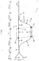
- FIG. 1 The exemplary embodiment of the inventive waveguide device of the present invention is shown in FIG. 1 and is designated generally by reference numeral 20.
- Athermalized integrated optical waveguide device 20 includes a first waveguide core arm 32 and a second waveguide core arm 34.
- First and second waveguide core arms 32 and 34 are comprised of a silica glass core composition.
- first and second waveguide core arms 32 and 34 are cladded with a waveguide cladding 38 comprised of a silica glass cladding composition.
- the silica glass core composition of first and second waveguide core arms 32 and 34 and the silica glass cladding composition of waveguide cladding 38 have a difference in boron concentration.
- the cladding composition and the core compositions have different boron concentrations, one of which may be zero.
- Boron is a silica glass index depressing dopant which reduces the thermal variation of the index of refraction. Boron is a dopant which provides for controlling the thermal spectral index shift slope (nm/°C), wherein the difference in boron concentration is a difference in concentration of dopant for controlling thermal spectral index shift slope (nm/°C).
- First waveguide core arm 32 is comprised of a path segment 42 having a waveguide core dimension of w 1 .
- Second waveguide core arm 34 is comprised of a path segment 44 having a waveguide core dimension of w 2 .
- dimensions w 1 and w 2 are waveguide core widths.
- the first waveguide core arm 32 of optical waveguide device 20 is comprised of a path segment 42 having a waveguide core width dimension of w 1 .
- the second waveguide core arm 34 is comprised of a path segment 44 having a waveguide core width dimensions of w 2 , wherein the widths w 1 and w 2 are not equal, and are substantially different.
- first waveguide core arm 32 is comprised of a path segment 42 which may have a waveguide core thickness dimension of w 1 .
- Second waveguide core arm 34 comprised of path segment 44 may have a waveguide core thickness dimension of w 2 .
- First waveguide core arm path segment 42 may have a waveguide core thickness and width dimensions different from second waveguide core arm path segment 44.
- the silica glass core composition of the invention is preferably comprised of GeO 2 , B 2 O 3 , P 2 O 5 , and SiO 2 . More preferably, the silica glass core composition comprises 10-20 wt.% GeO 2 , 0-2 wt.% B 2 O 3 , 0-2 wt.% P 2 O 5 , and 60-90 wt.% SiO 2 . Most preferably the silica glass core composition comprises about 15 wt.% GeO 2 , about 1 wt.% B 2 O 3 , about 1 wt.% P 2 O 5 , and about 83 wt.% SiO 2 .
- the silica glass cladding composition of the invention is preferably comprised of B 2 O 3 , P 2 O 5 , and SiO 2 . More preferably the silica glass cladding composition comprises 3-13 wt.% B 2 O 3 , 0-5 wt.% P 2 O 5 , and 75-97 wt.% SiO 2 . Most preferably the silica glass cladding composition comprises about 8 wt.% B 2 O 3 , about 2 wt.% P 2 O 5 , and about 90 wt% SiO 2 .
- the silica glass core composition and the silica glass cladding composition preferably have a boron concentration difference in the range of about 3 wt.% B 2 O 3 to about 11 wt.% B 2 O 3 .
- This boron concentration difference between the core and the cladding is more preferably in the range of about 5 wt.% B 2 O 3 to about 9 wt% B 2 O 3 , even more preferred in the range of about 6 wt.% B 2 O 3 to about 8 wt.% B 2 O 3 , and most preferably about 7 wt% B 2 O 3 .
- the first and second waveguide arms 32 and 34 are comprised of the same silica glass core composition with said first and second waveguide arms glass core compositions being formed concurrently from the same glass forming source, preferably as a uniform glass layer of homogeneous composition formed from a commonly mixed silica core glass feedstock which is convened preferably through oxidation into the glass.
- waveguide cladding 38 overlays first and second waveguide core arms 32 and 34 as a overclad layer of uniform composition formed from a commonly mixed silica cladding glass feedstock which is convened preferably through oxidation into the glass.
- the silica glass core composition is formed by flame hydrolysis conversion of a commonly mixed silica core glass feedstock comprised of halide-free organometallic source compounds.
- the silica glass cladding composition is formed by the flame hydrolysis conversion of a commonly mixed silica cladding glass feedstock comprised of halide-free organometallic source compounds.
- the source compound for SiO 2 is octamethylcyclotetrasiloxane
- GeO 2 is germanium ethoxide
- B 2 O 3 is triethylborate
- P 2 O 5 is trimethylphosphate.
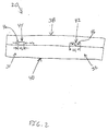
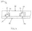
- Optical waveguide device 20 comprises a silica glass substrate 40, which provides a base for the formation of the device waveguides such as first and second waveguide core arms 32 and 34.
- Substrate 40 may comprise a silicon substrate having a buffer layer.
- first waveguide core arm path segment 42 having the waveguide core width w 1 is substantially parallel with the second waveguide core arm path segment 44 having the waveguide core width w 2 .
- first waveguide core arm 32 is not equal to the optical path length of second waveguide core arm 34.
- the physical path length of first waveguide core arm 32 is not equal to the physical path length of second waveguide core arm 34 as measured from Y coupler 30 to proximity coupler 36.
- a balanced Mach-Zehnder interferometer can be utilized where both arms are of equal physical length, but have unequal optical path length.
- first waveguide core arm 32 is comprised of path segments 46 having a waveguide core width of w 3 .
- First waveguide core arm 32 includes adiabatic tapers 48 between path segments 46 and path segment 42.
- Adiabatic tapers 48 connect the w 3 core width of path segment 46 with the w 1 core width of path segment 42.
- Second waveguide core arm 34 includes adiabatic tapers 50 between path segments 46 and path segment 44.
- Adiabatic tapers 50 connect the w 3 core width of path segment 46 with the w 2 core width of path segment 44.
- the length of first waveguide core arm path segment 42 having the w 1 waveguide core width is substantially equal to the length of second waveguide core arm path segment 44 having the w 2 waveguide core width.
- the invention further includes an integrated optical waveguide device 20.
- an athermalized Mach-Zehnder interferometer comprised of at least two unequal optical path length waveguide paths 32 and 34 of the same core glass composition comprised of GeO 2 , B 2 O 3 P 2 O 5 , and SiO 2 , which are cladded with a clad glass composition comprised of B 2 O 3 P 2 O 5 , and SiO 2 , having a B 2 O 3 concentration different than the core glass composition, wherein the at least two unequal length paths 32 and 34 include respectively path segments 42 and 44 of different path segment widths.
- the difference of widths between the path segments 42 of path 32 and 44 of path 34 provide a means for varying the fraction of the mode field propagated in the waveguide paths.
- the path segments 42 and 44 of different widths have the same length.
- the invention further includes an integrated optical waveguide interferometer comprising: a first channel waveguide arm and a second channel waveguide arm, said channel waveguide arms having a difference in length of ⁇ L, said channel waveguide arms comprised of a core composition, said first channel waveguide arm including a segment of length L w having a channel waveguide width w 1 and a mode field effective index N 1 dependent on the channel waveguide width w 1 , said first channel waveguide arm including a segment having a channel waveguide width w 3 and a mode field effective index N 3 dependent on the channel waveguide width w 3 , said second channel waveguide arm including a segment of length L w having a channel waveguide width w 2 and a mode field effective index N 2 dependent on the channel waveguide width w 2 , said second channel waveguide arm including a segment having a channel waveguide width w 3 and a mode field effective index N 3 dependent on the channel waveguide width w 3 , a waveguide cladding composition, said waveguide cladding composition cladding said
- the method of making the optical waveguide devices of the invention includes the method of athermalizing the optical waveguide devices to inhibit thermal spectral shifts.
- the inventive method of making an optical waveguide device includes the step of providing a first waveguide arm 32 and a second waveguide arm 34, with the waveguide arms having a difference in length of ⁇ L; the waveguide arms comprised of a core composition having a high index of refraction, the first waveguide arm including a segment 42 of length L w having a waveguide width w 1 , the remainder of said first waveguide arm having a waveguide width w 3 , the second waveguide arm 34 including a segment 44 of length L w having a waveguide width w 2 , and the remainder of said second waveguide arm having a waveguide width w 3 .
- the inventive method includes the step of cladding the waveguide arms with a cladding composition having a low index of refraction, said cladding composition having a boron concentration different from the boron concentration of the core composition, wherein ⁇ B is the difference between the boron concentration of the core composition and the cladding composition.
- the method further includes the step of athermalizing the optical waveguide device by optimizing ⁇ L, L w , w 1 , w 2 , w 3 , and ⁇ B to provide a zero or near zero thermal spectral shift when subjected to a change in temperature T.
- the segment 42 of length L w having a waveguide width w 1 has a mode field effective index N 1 dependent on the width w 1 .
- the segment 44 of length L w having a waveguide width w 2 has a mode field effective index N 2 dependent on the width w 2 .
- the remainder of the first and second waveguide arms 32 and 34 have a waveguide width of w 3 with a mode field effective index N 3 .
- the method of making the optical waveguide device includes the step of athermalizing the device by providing N 3 , ⁇ L, N 2 , N 1 , and L w according to the equation: dN 3 dT ⁇ L + d ( N 2 - N 1 ) dT L w ⁇ O
- the invention further includes a method of making an optical waveguide device 20 preferably a Mach-Zehnder interferometer embodied in an integrated optical circuit, having the step of providing an optical waveguide device substrate 40.
- the optical waveguide device substrate is comprised of silica glass, most preferably fused silica.
- the method further includes the step of forming a first waveguide core arm 32 of a silica glass core composition of high refractive index, first waveguide core arm 32 including a path segment 42 having a waveguide core width of w 1 and a path segment 46 having a waveguide core width of w 3 , first waveguide core arm 32 having a length of L 1 .
- the method includes the step of forming a second waveguide core arm 34 of said silica glass core composition, second waveguide core arm 34 including a path segment 44 having a waveguide core width of w 2 and a path segment 46 having a waveguide core width of w 3 , second waveguide core arm 34 having a length L 2 not equal to the length L 1 of first waveguide core arm 32.
- the method further includes the step of cladding first and second waveguide core arms 32 and 34 with a silica glass cladding composition of low refractive index.
- the method includes providing the silica glass core composition with a boron concentration B core .
- the method further includes the step of providing the silica glass cladding composition with a boron concentration B clad different from the silica glass core composition boron concentration B core .
- the step of forming first waveguide core arm 32 and second waveguide core arm 34 includes the step of depositing a core layer of the silica glass core composition over the silica glass substrate and the step of exposing the deposited core layer with an image containing a pattern of first waveguide core arm 32 and second waveguide core arm 34.
- this method utilizes photolithography techniques in which a mask containing the planar pattern of the waveguide arms and optical circuitry of optical waveguide device 20 including the appropriate size, orientation, placement, and shape of elements such as couplers 30 and 36, waveguide segments 46, 44, 42, adiabatic tapers 48 and 50, input waveguide 24, and output waveguides 26 and 28 is used with light to expose an image of the pattern on the core composition.
- Such light exposure effects a chemical change in the exposed areas compared to the unexposed areas.
- Chemical processing techniques such as etching, preferably reactive ion etching, are used to remove the exposed or unexposed areas to result in waveguide arms 32 and 34 and the other elements of optical waveguide device 20 and its optical circuitry.
- Exposure and removal techniques can be utilized to adjust the depth of formed waveguides and elements. Exposure and removal techniques can also be utilized to adjust the resolution, width, and other dimensions of the pattern image and the formed waveguides and elements.
- Such exposure, chemical processing, and removal techniques can be utilized to change and adjust the optical properties and characteristics of the wavguides, such as to change or adjust the optical path lengths of the waveguides.
- the method step of forming first waveguide core arm 32 and second waveguide core arm 34 includes the step of forming first waveguide core arm path segments 42 having a waveguide core width of w 1 substantially parallel to second waveguide core arm path segment 44 having a waveguide core width of w 2 .
- the method further includes forming first waveguide core arm path segment 42 having a waveguide core width of w 1 with a length of L w and second waveguide core arm path segment 44 having a waveguide core width of w 2 with a substantially equal length of L w .
- the method includes the step of optimizing w 3 , L 1 , L 2 , w 1 , w 2 , L w , and the difference between B core and B clad to provide an athermal optical waveguide device having a minimal or no dependence on temperature T, more preferably an athermal amplitude interferometer, and most preferably a Mach-Zehnder interferometer.
- An athermal Mach-Zehnder interferometer optical waveguide device 20 may be produced, utilizing straight waveguide path segments 42 and 44 having the same length L w and different widths, w 1 and w 2 , to vary the fraction of the mode field which is propagated within the core and clad layer compositions which have different boron concentrations, resulting in minimal temperature dependence.
- the same silica glass core composition is used for each of the interferometer arms 32 and 34.
- the same silica glass cladding composition is used to clad arms 32 and 34 with cladding 38.
- Straight waveguide path segment 42 having a waveguide core width of w 1 , of first waveguide core arm 32 and straight waveguide path segment 44 having a waveguide core width of w 2 of second waveguide core arm 34 have the same length L w , so that the path length difference ⁇ L between first waveguide core arm 32 and second waveguide core arm 34 is not changed but their different widths w 1 and w 2 vary the fraction of the mode field which is propagated within the core and clad layers which have a boron concentration difference ⁇ B.
- the preferred boron concentration B core of the silica glass core composition which comprises the core is 1 wt.% boron (B 2 O 3 ).
- Path segment 42 of waveguide core width w 1 and path segment 44 of waveguide core width w 2 are utilized in the invention without additional loss by providing adiabatic tapers 48 and 50 between the path segments of different width to couple these waveguides of different widths.
- Path segment 42 may have an enlarged width w 1 which may be multimode but this does not impact the response of the device because only the fundamental mode is excited and any residual light coupled to higher order modes is eliminated by waveguides 46 located after path segment 42.
- the length of waveguides 46 after path segments 42 and 44 may be increased as needed to obtain the filtering effect while not changing ⁇ L.
- OPD Optical Path Difference
- N 1 [ f ( w 1 )] N core +[1 - f ( w 1 )] N clad
- N 2 [ f ( w 2 )] N core + [1 - f ( w 2 )] N clad
- N 2 - N 1 [ f ( w 2 ) - f ( w 1 )][ N core - N clad ]
- the Mach-Zehnder interferometer silica glass core composition is comprised of 15.6 wt.% GeO 2 , 1.1 wt.% B 2 O 3 , 0.7 wt.% P 2 O 5 , and 82.6 wt.% SiO 2 , and has an index of refraction of approximately 1.455.
- the Mach-Zehnder interferometer silica glass cladding composition is comprised of 7.9 wt.% B 2 O 3 , 2.1 wt.% P 2 O 5 , and 90 wt.% SiO 2 , and has an index of refraction of approximately 1.444. These compositions are deposited on a fused silica substrate using flame hydrolysis deposition. Channel waveguides are patterned and formed using photolithography and reactive ion etching. As shown in FIG.
- Y coupler 30 having a length of about 2800 ⁇ m
- the temperature coefficient d ( N 2 - N 1 ) / dT is calculated from d 2 N/(dTdB) which is a factor that is representative of the core and clad materials and can be determined by analysis of the core and clad materials.
- L w 4000 ⁇ m.
- the path segments 42 and 44 comprise about 20% of the length of optical waveguide device 20.
- Athermalized waveguide device 20 may have more than two waveguide core arms.
- athermalized waveguide device 20 comprises a wavelength division multiplexer/demultiplexer
- athermalized waveguide device 20 may include a plurality of waveguide core arms.
- the plurality of waveguide core arms are in the form of a phased array, also known as a phasar.
- the phased array of waveguide core arms may include approximately a hundred waveguide core arms.
- FIG. 4 shows an example of an athermalized waveguide device 20 comprising a multiplexer/demultiplexer 120 which included a phased array 140 of waveguide core arms 32, 34, 103, 104, and 105.
- FIG. 4 provides an example of such a multiplexer/demultiplexer having only five waveguide core arms, wherein operation such a multiplexer/demultiplexer would include 3 or more waveguide core arms, and usually would include many more waveguide core arms, usually as many as about 100.
- Multiplexer/demultiplexer 120 as referenced in the direction for demultiplexing further includes couplers 130 and 136, waveguide input 201, and waveguide outputs 301, 302, 303, and 304.
- Coupler 130 may couple an optical signal comprised of four wavelength channels from input 201 into waveguide core arms 32, 34, 103, 104, and 105 which function to separate the optical signal into its four wavelength channels which are coupled by coupler 136 into outputs 301, 302, 303, and 304.
- waveguide core arm 32 is comprised of a path segment 42 having a waveguide core dimension of w 1 , path segments 46 having a waveguide core dimension w 3 , and adiabatic tapers 48 between path segments 46 and path segment 42.
- Waveguide core arm 34 is comprised of a path segment 44 having a waveguide core dimension of w 2 , path segments 46 having a waveguide core dimension w 3 , and adiabatic tapers 50 between path segments 46 and path segment 44.
- Waveguide core arm 103 is comprised of a path segment 146 having a waveguide core dimension w 103 , path segments 46 having a waveguide core dimension w 3 , and adiabatic tapers 152 between path segments 46 and path segment 146.
- Waveguide core arm 104 is comprised of a path segment 148 having a waveguide core dimension w 104 , path segments 46 having a standard waveguide core dimension w 3 , and adiabatic tapers 154 between path segments 46 and path segment 148.
- Waveguide core arm 105 is comprised of a path segment 150 having a waveguide core dimension w 105 , path segments 46 having a waveguide core dimension w 3 , and adiabatic tapers 156 between path segments 46 and path segment 150.
- First, second, third, fourth, and fifth waveguide core dimensions w 1 , w 2 , w 103 w 104 , and w 105 are unequal.
- FIG. 5 provides another embodiment of an athermalized waveguide device 20 comprising a multiplexer/demultiplexer 120.
- the phased array 140 of waveguide core arms 32, 34, 103, 104, and 105 include path segments 42 of varying length having a waveguide core arm dimension w 1 and path segments 44 of varying length having a waveguide core arm dimension w 2 , in a cascaded fashion with the sum of the lengths of path segment 42 and 44 being the same for the waveguide core arms.
- the length of path segment 42 in each of the waveguide core arms incrementally varies from the first waveguide core arm to the highest number waveguide core arm. Accordingly the length of path segment 44 increases as the length of path segment 42 decreases.
- Waveguide core arms 32, 34, 103, 104, and 105 include path segments 46 having a standard waveguide core arms dimension w 3 .
- Waveguide core arms 32, 34, 103, 104, and 105 include adiabatic tapers 50 between path segments 46 and path segments 44; adiabatic tapers 49 between path segments 44 and path segments 42; and adiabatic tapers 48 between path segments 42 and path segments 46.
- Multiplexer/demultiplexers 120 as shown in FIG. 4 and 5 are athermalized using principles of the invention as described in relation to the embodiment shown in FIG. 1.
- the phased array of waveguide core arms in a multiplexer/demultiplexer can be seen as an interferometer with more than two optical paths in the interferometric section, and may have up to about 100 waveguide core arms in the interferometric section.
- OPD optical path difference
- ⁇ L m ⁇ ; wherein N is the mode field effective index, ⁇ L is the path length increase, and m is an integer.
- the length of path segment 44 plus the length of path segment 42 is l .
- Path segment 42 has a mode field effective index N 1 associated to the waveguide width dimension of w 1 .
- Path segment 44 has an a mode field effective index N 2 associated to the waveguide width dimension of w 2 .
- Path segments 46 have a mode field effective index N 3 associated to the waveguide width dimension of w 3 .
- the lengths of path segment 42 and 44 are varied depending on the waveguide core arms position in the phased array.
- OPD optical path length difference
- Such athermalized multiplexer/demultiplexer may be made more compact by utilizing material compositions that provide a greater difference in thermal index shift slope (nm/°C) between the core composition and the cladding composition.
Priority Applications (2)
| Application Number | Priority Date | Filing Date | Title |
|---|---|---|---|
| EP98402132A EP0982607A1 (fr) | 1998-08-27 | 1998-08-27 | Dispositif de guide d'onde optique intégré athermique |
| US09/775,911 US20020154846A1 (en) | 1998-08-17 | 2001-02-02 | Athermal integrated optical waveguide device |
Applications Claiming Priority (1)
| Application Number | Priority Date | Filing Date | Title |
|---|---|---|---|
| EP98402132A EP0982607A1 (fr) | 1998-08-27 | 1998-08-27 | Dispositif de guide d'onde optique intégré athermique |
Publications (1)
| Publication Number | Publication Date |
|---|---|
| EP0982607A1 true EP0982607A1 (fr) | 2000-03-01 |
Family
ID=8235476
Family Applications (1)
| Application Number | Title | Priority Date | Filing Date |
|---|---|---|---|
| EP98402132A Withdrawn EP0982607A1 (fr) | 1998-08-17 | 1998-08-27 | Dispositif de guide d'onde optique intégré athermique |
Country Status (1)
| Country | Link |
|---|---|
| EP (1) | EP0982607A1 (fr) |
Cited By (1)
| Publication number | Priority date | Publication date | Assignee | Title |
|---|---|---|---|---|
| US6850654B2 (en) | 2001-02-09 | 2005-02-01 | Itf Optical Technologies Inc. | Passive thermal compensation of all-fiber Mach-Zehnder interferometer |
Citations (4)
| Publication number | Priority date | Publication date | Assignee | Title |
|---|---|---|---|---|
| US5295205A (en) * | 1993-03-29 | 1994-03-15 | Corning Incorporated | Environmentally stable monolithic Mach-Zehnder device |
| US5377285A (en) * | 1993-02-11 | 1994-12-27 | Honeywell Inc. | Technique for making ultrastable ring resonators and lasers |
| EP0793122A2 (fr) * | 1996-02-27 | 1997-09-03 | Hitachi Cable, Ltd. | Guide d'ondes optique, module optique et système optique l'utilisant |
| EP0849231A1 (fr) * | 1996-12-20 | 1998-06-24 | Corning Incorporated | Dispositif optique à guide d'onde codopé athermalisé |
-
1998
- 1998-08-27 EP EP98402132A patent/EP0982607A1/fr not_active Withdrawn
Patent Citations (4)
| Publication number | Priority date | Publication date | Assignee | Title |
|---|---|---|---|---|
| US5377285A (en) * | 1993-02-11 | 1994-12-27 | Honeywell Inc. | Technique for making ultrastable ring resonators and lasers |
| US5295205A (en) * | 1993-03-29 | 1994-03-15 | Corning Incorporated | Environmentally stable monolithic Mach-Zehnder device |
| EP0793122A2 (fr) * | 1996-02-27 | 1997-09-03 | Hitachi Cable, Ltd. | Guide d'ondes optique, module optique et système optique l'utilisant |
| EP0849231A1 (fr) * | 1996-12-20 | 1998-06-24 | Corning Incorporated | Dispositif optique à guide d'onde codopé athermalisé |
Cited By (1)
| Publication number | Priority date | Publication date | Assignee | Title |
|---|---|---|---|---|
| US6850654B2 (en) | 2001-02-09 | 2005-02-01 | Itf Optical Technologies Inc. | Passive thermal compensation of all-fiber Mach-Zehnder interferometer |
Similar Documents
| Publication | Publication Date | Title |
|---|---|---|
| US6256442B1 (en) | Athermal integrated optical waveguide device | |
| US5341444A (en) | Polarization compensated integrated optical filters and multiplexers | |
| Kawachi | Silica waveguides on silicon and their application to integrated-optic components | |
| AU716308B2 (en) | Article comprising a planar optical waveguide Mach-Zehnder interferometer device, and method of making same | |
| JP3766953B2 (ja) | 光回路 | |
| US6757454B2 (en) | Polarization desensitized optical waveguide interferometer | |
| JP3411818B2 (ja) | 光学導波路デバイスの製造方法 | |
| CA2245409C (fr) | Guide d'ondes optiques plan | |
| US6731828B2 (en) | Waveguide-type optical signal processing circuit | |
| US6950581B2 (en) | Optical coupler apparatus and methods having reduced geometry sensitivity | |
| De Peralta et al. | Reflective arrayed waveguide grating multiplexer | |
| US20020054294A1 (en) | Temperature insensitive mach-zehnder interferometers and devices | |
| JP2001519923A (ja) | 光学スペクトルに含まれるスペクトル光線を多重化解除する装置 | |
| WO2003038501A2 (fr) | Grille de guide d'ondes en reseau | |
| EP0982607A1 (fr) | Dispositif de guide d'onde optique intégré athermique | |
| WO1999021038A1 (fr) | Multiplexeur de longueurs d'onde a groupement a dephasage | |
| US20040151459A1 (en) | Method of polarisation compensation in grating- and phasar-based devices by using over-layer deposited on the compensating region to modify local slab waveguide birefringence | |
| US11372157B2 (en) | Integrated optical multiplexer / demultiplexer with thermal compensation | |
| JP3941613B2 (ja) | 光導波回路および光導波回路モジュール | |
| JP2003222748A (ja) | 光導波路型偏波分離素子及びその製造方法 | |
| JP3746776B2 (ja) | 導波路型光波長合分波器 | |
| JP3264652B2 (ja) | 光回路 | |
| JP4005520B2 (ja) | 光導波路素子 | |
| JP2000035523A (ja) | アレイ型導波路回折格子 | |
| JP2001091788A (ja) | 光合波分波器 |
Legal Events
| Date | Code | Title | Description |
|---|---|---|---|
| PUAI | Public reference made under article 153(3) epc to a published international application that has entered the european phase |
Free format text: ORIGINAL CODE: 0009012 |
|
| AK | Designated contracting states |
Kind code of ref document: A1 Designated state(s): DE FR GB IT SE |
|
| AX | Request for extension of the european patent |
Free format text: AL;LT;LV;MK;RO;SI |
|
| 17P | Request for examination filed |
Effective date: 20000412 |
|
| AKX | Designation fees paid |
Free format text: DE FR GB IT SE |
|
| 17Q | First examination report despatched |
Effective date: 20030401 |
|
| STAA | Information on the status of an ep patent application or granted ep patent |
Free format text: STATUS: THE APPLICATION IS DEEMED TO BE WITHDRAWN |
|
| 18D | Application deemed to be withdrawn |
Effective date: 20031014 |