EP0977249A2 - Verbesserte Methode zur Abscheidung eines Arsensilikatglasfilms auf einer Siliziumstruktur - Google Patents
Verbesserte Methode zur Abscheidung eines Arsensilikatglasfilms auf einer Siliziumstruktur Download PDFInfo
- Publication number
- EP0977249A2 EP0977249A2 EP99480049A EP99480049A EP0977249A2 EP 0977249 A2 EP0977249 A2 EP 0977249A2 EP 99480049 A EP99480049 A EP 99480049A EP 99480049 A EP99480049 A EP 99480049A EP 0977249 A2 EP0977249 A2 EP 0977249A2
- Authority
- EP
- European Patent Office
- Prior art keywords
- asg
- teasat
- film
- wafer
- teos
- Prior art date
- Legal status (The legal status is an assumption and is not a legal conclusion. Google has not performed a legal analysis and makes no representation as to the accuracy of the status listed.)
- Withdrawn
Links
Images


Classifications
-
- C—CHEMISTRY; METALLURGY
- C23—COATING METALLIC MATERIAL; COATING MATERIAL WITH METALLIC MATERIAL; CHEMICAL SURFACE TREATMENT; DIFFUSION TREATMENT OF METALLIC MATERIAL; COATING BY VACUUM EVAPORATION, BY SPUTTERING, BY ION IMPLANTATION OR BY CHEMICAL VAPOUR DEPOSITION, IN GENERAL; INHIBITING CORROSION OF METALLIC MATERIAL OR INCRUSTATION IN GENERAL
- C23C—COATING METALLIC MATERIAL; COATING MATERIAL WITH METALLIC MATERIAL; SURFACE TREATMENT OF METALLIC MATERIAL BY DIFFUSION INTO THE SURFACE, BY CHEMICAL CONVERSION OR SUBSTITUTION; COATING BY VACUUM EVAPORATION, BY SPUTTERING, BY ION IMPLANTATION OR BY CHEMICAL VAPOUR DEPOSITION, IN GENERAL
- C23C16/00—Chemical coating by decomposition of gaseous compounds, without leaving reaction products of surface material in the coating, i.e. chemical vapour deposition [CVD] processes
- C23C16/22—Chemical coating by decomposition of gaseous compounds, without leaving reaction products of surface material in the coating, i.e. chemical vapour deposition [CVD] processes characterised by the deposition of inorganic material, other than metallic material
- C23C16/30—Deposition of compounds, mixtures or solid solutions, e.g. borides, carbides, nitrides
- C23C16/40—Oxides
- C23C16/401—Oxides containing silicon
-
- H—ELECTRICITY
- H10—SEMICONDUCTOR DEVICES; ELECTRIC SOLID-STATE DEVICES NOT OTHERWISE PROVIDED FOR
- H10B—ELECTRONIC MEMORY DEVICES
- H10B12/00—Dynamic random access memory [DRAM] devices
- H10B12/01—Manufacture or treatment
- H10B12/02—Manufacture or treatment for one transistor one-capacitor [1T-1C] memory cells
- H10B12/03—Making the capacitor or connections thereto
- H10B12/038—Making the capacitor or connections thereto the capacitor being in a trench in the substrate
-
- H10P14/6548—
-
- H10P14/6922—
-
- H10W10/041—
-
- H10W10/40—
-
- H10P14/6334—
-
- H10P14/6923—
Definitions
- the present invention relates to the manufacture of semiconductor integrated circuits (ICs) and more particularly to an improved method of forming an arsenic silicon glass (ASG) film having an uniform thickness onto a silicon structure.
- the method finds a very useful application in the conformal deposition of such an ASG film in deep trenches formed in a silicon substrate to provide the necessary doping to create the buried plate region of cell capacitors.
- Deep trench cell capacitors are extensively employed in EDO (extended data out) and SDRAM (synchronous dynamic random access memory) memory chips. This process improvement significantly reduces chip manufacturing costs.
- a deep trench is formed in a slightly doped silicon substrate, then a thin dielectric film is conformally deposited thereon to coat the entire interior trench surface and finally, the trench is filled with doped polysilicon.
- This silicon substrate/dielectric film/doped polysilicon composite structure forms the cell capacitor.
- the thickness of the dielectric film is constantly reduced. In turn, the voltage across the dielectric film must be drastically reduced to avoid undesired voltage breakdown effects.
- a doped area is created in the silicon substrate around the bottom of the cell capacitor.
- This area is commonly referred to as the "buried plate” (BP) region in the technical literature.
- an arsenic silicon glass (ASG) film is conformally deposited onto the chip surface to coat the trench side wall and will be subsequently used to generate the arsenic (As) atoms to heavily dope the silicon substrate in order to create these BP regions.
- a conventional buried plate region formation process specifically includes the eight basic steps recited below.
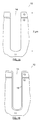
- Fig. 1A schematically illustrates the starting structure 10 consisting of a p-type silicon substrate 11 with a 10 nm thick silicon oxide layer 12 and a 220 nm thick silicon nitride layer 13 formed thereon. These two layers will be referenced to hereinbelow as the Si02/Si3N4 pad layer 12/13.
- a deep trench referenced 14 has been formed in the substrate 11 by RIE etching as standard.
- deep trench 14 has a depth of about 7 ⁇ m and an oblong section of about 550 x 320 nm at the substrate surface.
- an arsenic silicon glass is conformally deposited by LPCVD to coat the interior trench side wall with a 45 nm thick film referenced 15.
- ASG film 15 As known for those skilled in the art, As atoms contained in ASG film 15 will subsequently act as N type dopants.
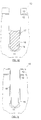
- This step is performed in a deposition equipment such as a vertical hot dual wall SVG 7000+ LPCVD reactor manufactured and sold by SVG THERMCO, Orange, CA, USA, schematically illustrated in Fig. 3 that will be detailed later on.
- the reactive atmosphere includes tetraethylorthosilicate (TEOS) and triethylarsenate (TEASAT) gases.
- TEOS tetraethylorthosilicate
- TEASAT triethylarsenate
- a 1.8 ⁇ m thick layer of a planarizing medium typically a photoresist
- a planarizing medium typically a photoresist
- a photoresist such as AZ7511 manufactured by CLARIANT, Brunswick, NJ, USA, is adequate in that respect.
- the photoresist layer bearing numeral 16 has a planar surface.
- photoresist layer 16 After photoresist reflow was performed, a given amount of the photoresist material is removed by a conventional lithographic process, so that the surface of photoresist layer 16 stands at about 1.5 ⁇ m below the structure surface. The remaining material of photoresist layer 16 exhibits a typical recessed shape at its upper surface in trench 14 as shown in Fig. 1D.
- the unprotected portions of the N+ doped ASG film 15 are removed by wet etching in a buffered HF bath.
- An overetching occurs during this wet etch step at the top annular portion of the ASG film 15 to produce the moat or dip out 17, as apparent in Fig. 1E.
- the photoresist material remaining at the bottom of deep trench 14 is stripped by wet etching in a Huang SP solution and a 25 nm thick Si02 layer 18 is conformally deposited by PECVD onto the structure to coat the deep trench side wall.
- a Huang SP solution a 25 nm thick Si02 layer 18 is conformally deposited by PECVD onto the structure to coat the deep trench side wall.
- An AME 5000 tool commercially available from Applied Materials Inc., Santa Clara, CA, USA is appropriate. After these two process steps have been performed, the structure 10 is shown in Fig. 1F.
- the structure 10 is then heated to diffuse the As doping atoms trapped in the ASG film 15 into the adjacent portions of the silicon substrate 11 to create the buried plate region 19.
- the structure 10 is shown in Fig. 1G.
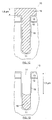
- Fig. 2 shows structure 10 after gate conductor stack and source/drain regions completion.
- the Si02/Si3N4 pad layer 12/13 has been eliminated and the trench 14 has been filled with doped polysilicon to form the first electrode of the cell capacitor.
- the polysilicon fill 20 is electrically isolated from the substrate 11 by a 30 nm thick TEOS SiO2 collar layer 21 on its upper part and a 5 nm thick reoxidized silicon nitride layer 22 on its lower part. The latter layer forms the dielectric film of the cell capacitor.
- two ion implantation steps are performed to define first a 1000 nm thick N-well 23, then a 800 nm thick P-well region 24.
- the second electrode of the cell capacitor is thus formed by the buried plate region 19, the N-well region 23 being used to interconnect all the buried plate regions of the chip.
- an IGFET bearing numeral 27 visible in Fig. 2 is created.
- the top of BP region 19 is located below and preferably at about 450 nm from the P-well/N-well junction. If the top of BP region 19 extends in the P-well region, a parasitic NPN transistor is then constituted by the N type drain region 26 of IGFET 27, the P-well 24 and the N+ BP region 19 that will degrade the storage operation. If the top of BP region 19 is below the bottom of N-well region 23, the BP region 19 could not be biased via the N-well 23 any longer and undesired voltage breakdown would occur during storage operation. As a consequence, it is recommended to have the top of the BP region 19 centered in the N-well at 1250 nm +- 450 nm from silicon substrate 11 surface.
- the targeted value for photoresist etch is 1500 nm +- 250 nm which corresponds to the value indicated in Fig. 1D.
- the step of partially removing the photoresist material of layer 16 is thus essential to the whole buried plate region formation process because the remaining photoresist determines the protected portions of the ASG film to remain which in turn defines the BP region during the out diffusion step.
- the vertical reactor referenced 30 is essentially comprised of outer and inner walls 31 and 32 affixed upon a base 33.
- the temperature inside the reactor is controlled by a five heating zone element 34.
- a boat 35 containing the wafers 36 is mounted on a pedestal 37 in the central part of the base 33.
- An exhaust pump 38 is connected to the interior volume of the reactor by adequate piping.
- Reactor 30 further includes a TEASAT bubbler system 39 and a TEOS vapor delivery system 40.
- the reactor has two separated bottom gas injections for the TEOS and TEASAT lines at opposite side of the base 33.
- the TEOS vapor delivering system and the TEASAT bubbler are manufactured by Schumacher, Carlsbad, CA, USA, which also supplies the TEASAT precursor.
- the TEOS gas is produced by heating liquid TEOS in an ampule at 65°C (supplied by OLIN HUNT, Seeward, ILL, USA).
- vapor is fabricated by nitrogen bubbling in a 45°C heated liquid TEASAT ampule (manufactured by Schumacher).
- the diameters of the injection lines are equal to .25 inch.
- TEOS and TEASAT precursors delivery gas lines and nitrogen bubbling line are all heated up to 80°C to avoid gas condensation into liquid droplets before injection.
- the process parameters are: Bubbler Temp.
- This sheet resistivity of 150 Ohm/sq which is the greatest acceptable value corresponds to an As atom concentration of about 5E19 at/cm3 in the ASG film 15 .
- the conventional ASG film deposition process mentioned above produces ASG film side wall thickness of 45 nm (+- 15% wafer to wafer, +-7% within a same wafer) and an As concentration varying between 1E21 and 2E21.
- the junction depth and the As concentration in BP region 19 can be out of specifications (below the desired values of .25 ⁇ m and 5E19 at/cm3 respectively).
- the top location of BP region 19 can be not well centered. As emphasized above, the BP region 19 top location spreads so much within the chip with the conventional process that this is dramatic for chip reliability.
- BP region 19 will be too low.
- As concentration is too low (not enough doping species)
- the BP region 19 is not well formed and the cell capacitor breakdown occurs at lower VT (threshold voltage).
- ASG arsenic silicon glass
- the method of the present invention aims to get rid of the drawbacks inherent to the conventional method of forming an arsenic silicon glass (ASG) film onto a silicon structure by LPCVD from TEOS and TEASAT precursors.
- ASG arsenic silicon glass
- TEOS TEOS
- TEASAT TEASAT precursors
- Fig. 1A to 1H show a state-of-the-art structure consisting of a silicon substrate provided with a deep trench undergoing the essential steps of a conventional buried plate region formation process.
- Fig. 2 shows the structure substantially at the end of the deep trench cell capacitor fabrication process after gate stack conductor and source/drain region formation to emphasize the critical aspects of the buried plate region formation process and control thereof.
- Fig. 3 schematically shows a conventional vertical hot dual wall LPCVD reactor incorporating a common N2/O2 injection line according to the method of the present invention.
- Figs. 4 (A) and 4(B) are graphs depicting the thickness and the As atom concentration variations along the LPCVD reactor with the conventional and the improved method of the present invention respectively.
- the ASG film deposition is obtained by reacting a mixture of TEOS (TetraEthylOrthoSilicate) and TEASAT (TriEthylArsenate) in a gaseous phase and in a LPCVD reactor.
- the TEOS gas is flowing into the process chamber and the TEASAT gas is carried into the reactor through N2 bubbling.
- Applicant's inventors have discovered that the poor thickness and As concentration uniformity of the ASG film resulted of a fast and immediate reaction between TEOS and TEASAT precursors which react together according to an uncontrollable kinetics as soon as they are injected.
- the TEASAT molecule takes some oxygen atoms from the TEOS molecules to form the desired arsenic oxide (As2O5) in the ASG material, but because the TEOS thermal decomposition is catalyzed by the TEASAT presence (this reaction is called "interactive co-pyrolysis"), the chemical reaction is not homogeneous all along the vertical reactor. They have remarked that the co-pyrolysis is much faster at the injection zone (bottom of the reactor) than at the exhaust zone (top of the reactor). So that the arsenic carrying reactant (TEASAT) is getting poorer and poorer as it travels across the vertical reactor, and the two key process parameters mentioned above, i.e. the ASG film thickness and As dopant concentration in the ASG film become extremely hard to control.
- Fig. 4(A) shows the variation of the thickness (curve 41) and of the As concentration (curve 42) along the vertical reactor of Fig. 3 (conventional version) in its active area represented by distance L.
- the reaction is correctly controlled while it is not in the extreme zones I and III resulting in poor ASG film thickness uniformity wafer to wafer (zone I) and As concentration uniformity within a same wafer (zone III).
- the O2/N2 common injection line is heated up to 80°C to avoid gas condensation into liquid droplets in the lower part of reactor 30. Note also that the diameter of the O2/N2 common line has been set to .25 inch to augment the gas velocity and the TEASAT line diameter increased to .5 inch.
- Fig. 4(B) shows the ASG film thickness and As atoms concentration that are now obtained with the method of the present invention.
- Fig. 4(B) where these profiles are illustrated by curves 43 and 44 respectively.
- Fig. 4(B) it is apparent that both profiles are more flat along the totality of the reactor length L.
- the depletion of the TEASAT reactant does not occur anymore because the TEASAT need of oxygen is now supplied by another source and no longer by the TEOS precursor, so that the TEOS/TEASAT/O2 co-pyrolysis becomes non-interactive.
- the reactants have then a separate thermal decomposition as soon they are injected, leading to a more uniform ASG film deposition by bringing enough As atoms at the top of the reactor and slowing the total decomposition rate.
- the deposition rate still reaches 1.1 nm/min but now with a total thickness control.
- the ASG film thickness is in the 45 nm +- 3% range (wafer to wafer) and is achieved across the totality of the 75 product wafer load. Thickness uniformity within wafer is less than 2.5% at three sigma ensuring thereby a very good layer uniformity trench to trench across the chip and is easily kept on the 75 product wafers of the batch. Film conformality is about 55% that is 5 to 7 % better than with the conventional process.
- the arsenic concentration in the ASG film is measured with a Rigaku 3630 (manufactured by RIGAKU, Osaka, Japan). It varies from 9 at the bottom of the reactor to 6.5 As w% at its top instead of a 12 to 2 As w% range with the conventional process.
- This invention not only allows to get rid of thickness and As concentration non-uniformity along the reactor but also brings foreign particles (FM) at an outstandingly low level ( ⁇ 20 particles per monitor wafer) and produces high glass purity (very low level of Carbon and OH radicals) probably because the chemical reaction is more complete. That yield improvement decreases the amount of a glassy solid formed with a byproducts mixture condensation which is clogging exhaust piping and at last aborting tool performance. Then, the reactor downtime is drastically reduced.
- FM foreign particles
- the process of the present invention is much better controlled.
- the quality of deposited ASG film is then improved (conformality, thickness and As concentration distribution uniformity and finally purity).
- the Arsenic atoms incorporated in the ASG film, vehicle of the buried plate region formation are better carried in gaseous phase across the totality of the reactor length and its concentration in the ASG film is nearly independent of the patterned wafer surface. Consequently, the present method could be applied to next product generations and the deep trench cell capacitor life could be extended.
- the non-interactive copyrolysis thanks to the O2 presence improves the process step manufacturability by batch size/process speed increasing and LPCVD tool downtime lowering.
- the method of the present invention meets the following advantages:
Landscapes
- Chemical & Material Sciences (AREA)
- Engineering & Computer Science (AREA)
- Manufacturing & Machinery (AREA)
- Inorganic Chemistry (AREA)
- General Chemical & Material Sciences (AREA)
- Chemical Kinetics & Catalysis (AREA)
- Materials Engineering (AREA)
- Mechanical Engineering (AREA)
- Metallurgy (AREA)
- Organic Chemistry (AREA)
- Formation Of Insulating Films (AREA)
- Semiconductor Memories (AREA)
Priority Applications (1)
| Application Number | Priority Date | Filing Date | Title |
|---|---|---|---|
| EP99480049A EP0977249A3 (de) | 1998-07-31 | 1999-07-01 | Verbesserte Methode zur Abscheidung eines Arsensilikatglasfilms auf einer Siliziumstruktur |
Applications Claiming Priority (3)
| Application Number | Priority Date | Filing Date | Title |
|---|---|---|---|
| EP98480051 | 1998-07-31 | ||
| EP98480051 | 1998-07-31 | ||
| EP99480049A EP0977249A3 (de) | 1998-07-31 | 1999-07-01 | Verbesserte Methode zur Abscheidung eines Arsensilikatglasfilms auf einer Siliziumstruktur |
Publications (2)
| Publication Number | Publication Date |
|---|---|
| EP0977249A2 true EP0977249A2 (de) | 2000-02-02 |
| EP0977249A3 EP0977249A3 (de) | 2003-07-16 |
Family
ID=26151818
Family Applications (1)
| Application Number | Title | Priority Date | Filing Date |
|---|---|---|---|
| EP99480049A Withdrawn EP0977249A3 (de) | 1998-07-31 | 1999-07-01 | Verbesserte Methode zur Abscheidung eines Arsensilikatglasfilms auf einer Siliziumstruktur |
Country Status (1)
| Country | Link |
|---|---|
| EP (1) | EP0977249A3 (de) |
Cited By (1)
| Publication number | Priority date | Publication date | Assignee | Title |
|---|---|---|---|---|
| CN117153785A (zh) * | 2023-10-27 | 2023-12-01 | 合肥晶合集成电路股份有限公司 | 一种半导体结构的制作方法 |
Family Cites Families (6)
| Publication number | Priority date | Publication date | Assignee | Title |
|---|---|---|---|---|
| KR870000750A (ko) * | 1985-06-14 | 1987-02-20 | 이마드 마하윌리 | 이산화실리콘 필름을 화학적으로 증기피복하는 방법 |
| US4755486A (en) * | 1986-12-11 | 1988-07-05 | Siemens Aktiengesellschaft | Method of producing a defined arsenic doping in silicon semiconductor substrates |
| EP0491975A1 (de) * | 1990-12-21 | 1992-07-01 | Siemens Aktiengesellschaft | Verfahren zur Erzeugung einer definierten Arsendotierung in geätzten Gräben in Silizium-Halbleitersubstraten |
| US5387557A (en) * | 1991-10-23 | 1995-02-07 | F. T. L. Co., Ltd. | Method for manufacturing semiconductor devices using heat-treatment vertical reactor with temperature zones |
| JPH08186081A (ja) * | 1994-12-29 | 1996-07-16 | F T L:Kk | 半導体装置の製造方法及び半導体装置の製造装置 |
| US5746591A (en) * | 1996-08-15 | 1998-05-05 | Vanguard International Semiconductor Corporation | Semiconductor furnace for reducing particulates in a quartz tube and boat |
-
1999
- 1999-07-01 EP EP99480049A patent/EP0977249A3/de not_active Withdrawn
Non-Patent Citations (2)
| Title |
|---|
| BECKER F S, PAWLIK D, ANZINGER H, SPITZER A: "Low-pressure deposition of high-quality SiO2 films by pyrolysis of tetraethylorthosilicate", JOURNAL OF VACUUM SCIENCE AND TECHNOLOGY B, vol. 5, no. 6, 1 December 1987 (1987-12-01), pages 1555 - 1563, XP000008339 * |
| XIE J; MCBRIDE M; HAINES J C: "Negative bias-temperature instability study of silicon oxide and its impact on PMOS reliability", PROCEEDINGS OF THE SPIE - THE INTERNATIONAL SOCIETY FOR OPTICAL ENGINEERING, MICROELECTRONIC MANUFACTURING YIELD, RELIABILITY, AND FAILURE ANALYSIS; 25-26 OCT 1995; AUSTIN, TX, USA, 25 October 1995 (1995-10-25), pages 96 - 101 * |
Cited By (2)
| Publication number | Priority date | Publication date | Assignee | Title |
|---|---|---|---|---|
| CN117153785A (zh) * | 2023-10-27 | 2023-12-01 | 合肥晶合集成电路股份有限公司 | 一种半导体结构的制作方法 |
| CN117153785B (zh) * | 2023-10-27 | 2024-03-01 | 合肥晶合集成电路股份有限公司 | 一种半导体结构的制作方法 |
Also Published As
| Publication number | Publication date |
|---|---|
| EP0977249A3 (de) | 2003-07-16 |
Similar Documents
| Publication | Publication Date | Title |
|---|---|---|
| US5998289A (en) | Process for obtaining a transistor having a silicon-germanium gate | |
| US7713881B2 (en) | Process sequence for doped silicon fill of deep trenches | |
| US4873205A (en) | Method for providing silicide bridge contact between silicon regions separated by a thin dielectric | |
| US20010014521A1 (en) | Batch processing for semiconductor wafers to form aluminum nitride and titanium aluminum nitride | |
| US6218319B1 (en) | Method of forming an arsenic silicon glass film onto a silicon structure | |
| US5591667A (en) | Method for fabricating MOS transistor utilizing doped disposable layer | |
| US6057216A (en) | Low temperature diffusion process for dopant concentration enhancement | |
| EP0150088B1 (de) | Halbleiteranordnung mit einer dielektrischen Schicht | |
| US20040266197A1 (en) | Methods of forming layers over substrates; and methods of forming trenched isolation regions | |
| US6806173B1 (en) | Method for producing highly doped semiconductor components | |
| KR20040002947A (ko) | 반도체 집적회로장치 및 그 제조방법 | |
| US5324686A (en) | Method of manufacturing semiconductor device using hydrogen as a diffusion controlling substance | |
| EP0977249A2 (de) | Verbesserte Methode zur Abscheidung eines Arsensilikatglasfilms auf einer Siliziumstruktur | |
| US5869406A (en) | Method for forming insulating layers between polysilicon layers | |
| KR100796724B1 (ko) | 커패시터 및 이의 제조 방법 | |
| US7189659B2 (en) | Method for fabricating a semiconductor device | |
| EP0429885B1 (de) | Verfahren der in-situ-Dotierung von abgeschiedenem Silizium | |
| US8202806B2 (en) | Method to avoid threshold voltage shift in thicker dielectric films | |
| US6784117B2 (en) | Method for manufacturing a semiconductor device | |
| EP0321746B1 (de) | Methode zur Ausbildung eines Brückenkontaktes zwischen Gebieten, die durch ein dünnes Dielektrikum getrennt sind | |
| JP3034263B2 (ja) | 薄膜形成装置 | |
| US6180539B1 (en) | Method of forming an inter-poly oxide layer | |
| JP2846671B2 (ja) | 半導体装置の製造方法およびその装置 | |
| US5712176A (en) | Doping of silicon layers | |
| KR100530149B1 (ko) | 반도체 소자의 게이트 전극 제조 방법 |
Legal Events
| Date | Code | Title | Description |
|---|---|---|---|
| PUAI | Public reference made under article 153(3) epc to a published international application that has entered the european phase |
Free format text: ORIGINAL CODE: 0009012 |
|
| AK | Designated contracting states |
Kind code of ref document: A2 Designated state(s): AT BE CH CY DE DK ES FI FR GB GR IE IT LI LU MC NL PT SE |
|
| AX | Request for extension of the european patent |
Free format text: AL;LT;LV;MK;RO;SI |
|
| PUAL | Search report despatched |
Free format text: ORIGINAL CODE: 0009013 |
|
| AK | Designated contracting states |
Designated state(s): AT BE CH CY DE DK ES FI FR GB GR IE IT LI LU MC NL PT SE |
|
| AX | Request for extension of the european patent |
Extension state: AL LT LV MK RO SI |
|
| 17P | Request for examination filed |
Effective date: 20030902 |
|
| 17Q | First examination report despatched |
Effective date: 20031023 |
|
| AKX | Designation fees paid |
Designated state(s): DE FR GB IE |
|
| 17Q | First examination report despatched |
Effective date: 20031023 |
|
| STAA | Information on the status of an ep patent application or granted ep patent |
Free format text: STATUS: THE APPLICATION IS DEEMED TO BE WITHDRAWN |
|
| 18D | Application deemed to be withdrawn |
Effective date: 20080902 |