EP0974187B1 - Impulsgenerator mit hohem wirkungsgrad zur erzeugung von kurzen spannungsimpulsen - Google Patents
Impulsgenerator mit hohem wirkungsgrad zur erzeugung von kurzen spannungsimpulsen Download PDFInfo
- Publication number
- EP0974187B1 EP0974187B1 EP98920510A EP98920510A EP0974187B1 EP 0974187 B1 EP0974187 B1 EP 0974187B1 EP 98920510 A EP98920510 A EP 98920510A EP 98920510 A EP98920510 A EP 98920510A EP 0974187 B1 EP0974187 B1 EP 0974187B1
- Authority
- EP
- European Patent Office
- Prior art keywords
- terminal
- switch
- voltage
- diode
- load
- Prior art date
- Legal status (The legal status is an assumption and is not a legal conclusion. Google has not performed a legal analysis and makes no representation as to the accuracy of the status listed.)
- Expired - Lifetime
Links
- 239000003990 capacitor Substances 0.000 claims description 37
- 238000011084 recovery Methods 0.000 claims 2
- 230000005284 excitation Effects 0.000 description 31
- 238000002604 ultrasonography Methods 0.000 description 12
- 230000001105 regulatory effect Effects 0.000 description 6
- 230000033228 biological regulation Effects 0.000 description 3
- 230000010355 oscillation Effects 0.000 description 3
- 239000004020 conductor Substances 0.000 description 2
- 238000010276 construction Methods 0.000 description 1
- 230000001276 controlling effect Effects 0.000 description 1
- 238000010586 diagram Methods 0.000 description 1
- 230000000694 effects Effects 0.000 description 1
- 230000006698 induction Effects 0.000 description 1
- 230000005415 magnetization Effects 0.000 description 1
- 239000000463 material Substances 0.000 description 1
- 238000000034 method Methods 0.000 description 1
- 230000003287 optical effect Effects 0.000 description 1
- 230000005693 optoelectronics Effects 0.000 description 1
- 239000004065 semiconductor Substances 0.000 description 1
- XLYOFNOQVPJJNP-UHFFFAOYSA-N water Substances O XLYOFNOQVPJJNP-UHFFFAOYSA-N 0.000 description 1
Images



Classifications
-
- H—ELECTRICITY
- H02—GENERATION; CONVERSION OR DISTRIBUTION OF ELECTRIC POWER
- H02M—APPARATUS FOR CONVERSION BETWEEN AC AND AC, BETWEEN AC AND DC, OR BETWEEN DC AND DC, AND FOR USE WITH MAINS OR SIMILAR POWER SUPPLY SYSTEMS; CONVERSION OF DC OR AC INPUT POWER INTO SURGE OUTPUT POWER; CONTROL OR REGULATION THEREOF
- H02M3/00—Conversion of DC power input into DC power output
- H02M3/02—Conversion of DC power input into DC power output without intermediate conversion into AC
- H02M3/04—Conversion of DC power input into DC power output without intermediate conversion into AC by static converters
- H02M3/10—Conversion of DC power input into DC power output without intermediate conversion into AC by static converters using discharge tubes with control electrode or semiconductor devices with control electrode
- H02M3/145—Conversion of DC power input into DC power output without intermediate conversion into AC by static converters using discharge tubes with control electrode or semiconductor devices with control electrode using devices of a triode or transistor type requiring continuous application of a control signal
- H02M3/155—Conversion of DC power input into DC power output without intermediate conversion into AC by static converters using discharge tubes with control electrode or semiconductor devices with control electrode using devices of a triode or transistor type requiring continuous application of a control signal using semiconductor devices only
- H02M3/156—Conversion of DC power input into DC power output without intermediate conversion into AC by static converters using discharge tubes with control electrode or semiconductor devices with control electrode using devices of a triode or transistor type requiring continuous application of a control signal using semiconductor devices only with automatic control of output voltage or current, e.g. switching regulators
- H02M3/158—Conversion of DC power input into DC power output without intermediate conversion into AC by static converters using discharge tubes with control electrode or semiconductor devices with control electrode using devices of a triode or transistor type requiring continuous application of a control signal using semiconductor devices only with automatic control of output voltage or current, e.g. switching regulators including plural semiconductor devices as final control devices for a single load
-
- H—ELECTRICITY
- H02—GENERATION; CONVERSION OR DISTRIBUTION OF ELECTRIC POWER
- H02M—APPARATUS FOR CONVERSION BETWEEN AC AND AC, BETWEEN AC AND DC, OR BETWEEN DC AND DC, AND FOR USE WITH MAINS OR SIMILAR POWER SUPPLY SYSTEMS; CONVERSION OF DC OR AC INPUT POWER INTO SURGE OUTPUT POWER; CONTROL OR REGULATION THEREOF
- H02M1/00—Details of apparatus for conversion
- H02M1/0067—Converter structures employing plural converter units, other than for parallel operation of the units on a single load
- H02M1/007—Plural converter units in cascade
Definitions
- the pulse generator for excitation of current pulses belongs to one Ultrasonic position sensor, consisting of a waveguide (41) in which a Ultrasound pulse is excited by a current pulse and transmitted to one Ultrasonic excitation circuit (4) in which the current pulse (27) through a electrical voltage pulse (30) is excited, a magnet (40) thereof Magnetic field in connection with the current pulse triggers the ultrasonic pulse and a detector (36, 37, 38, 39) for receiving the ultrasound pulse at one End of the waveguide.
- the transit time of the ultrasonic pulse through the Waveguide starting with the generation of the current pulse until reception through the detector is a measure of the magnetic position to be measured.
- the pulse generator can be advantageous for generating voltage and Current pulses on optoelectronic components or piezoelectric Actuators are used.
- the US 5,587,680 describes a pulse generator with a charge pump, which by Voltage doubling with switched capacitors a pulse output voltage generated that is higher than the input voltage supplied.
- the capacitors are made in parallel from the regulated charging voltage DC voltage source charged and connected in series to generate pulses.
- Disadvantage of the doubler circuit described is that a constant, of independent output voltage to fluctuations in the input voltage first achieve the input voltage at a defined voltage value must be reduced. This is done through linear regulation and causes power loss in the DC voltage source Disadvantage that the voltage only in integer multiples of the regulated DC voltage can be increased according to the number of cascade elements can.
- the pulse generator is used to generate electrical voltage pulses on a load element (4), preferably for excitation of current pulses in the Current pulse excitation circuit (4) of a known ultrasonic position sensor shown in FIG. 3 (35).
- the current pulse excitation circuit with a first (31) and second (34) connection consists of a current conductor (42), the current pulses (27) along the waveguide and back.
- the waveguide (41) itself can be part the current conductor (42). Interacting with the magnetic field of one Magnets (40) become ultrasound pulses in the ultrasound waveguide through the current pulses (41) generated.
- the ultrasonic pulses are in the ultrasonic waveguide passed on and at the end of which consists of a detector evaluated from a coil (38) and a signal processing unit (36).
- the Signal processing unit receives an electrical received from the coil Signal (37) and generates an electrical position signal (39) in known manner by measuring the transit time of the ultrasonic signal from the Position of the magnet (40) guided along the waveguide (41) up to Detector results.
- Other uses of the pulse generator, as well as others Load elements, e.g. Load impedances, semiconductor components, optical Components or piezoelectric actuators are possible.
- a voltage step-up (2) in Fig. 1 according to claims 3 to 8 consists of an inductor (16), a first switch (19), a second switch (17) and a storage capacitor (20).
- the first connection of the inductor is an input voltage (12) is supplied, the second terminal of the inductor with the first switch connection of the first switch and with the first Switch connection of the second switch connected.
- the second switching connection of the second switch (17) is connected to the first terminal of the Storage capacitor (20), the second terminal of the storage capacitor connected to the reference potential (11).
- the second switching connection of the first Switch is connected to the reference potential.
- the first switch (19) generates, according to claim 7, an N-channel MOSFET or bipolar transistor, approximately triangular current pulses (13) in the Inductance (16).
- a part of the water flows through self-induction Current pulses (18) through the first switch.
- the second switch according to claim 6 a diode, leads the current pulses generated in the inductor Storage capacitor (20) too.
- a decaying by self-induction flows Part of the current pulses (14) through the second switch.
- the current impulses generate an output voltage (15) applied to the storage capacitor, which is greater than or equal to the input voltage (12) supplied.
- An alternative embodiment of a voltage step-up (2) in Fig. 4 after Claim 20 consists of an inductor (45), a first switch (43), a second switch (44) and the storage capacitor (20).
- the interconnection of the Components correspond to the aforementioned embodiment, but are Places of inductance and first switch compared to the aforementioned Embodiment interchanged.
- the first switch is preferably a P-channel MOSFET or a PNP bipolar transistor
- the second switch is preferred a diode (44) and polarized in relation to the aforementioned embodiment, that negative current pulses are supplied to the storage capacitor.
- the Output voltage of this embodiment is negative and the amount greater than or equal to the input voltage supplied.
- FIG 6 and 7 Two further alternative embodiments of a voltage step-up in FIG 6 and 7 according to claims 21 and 22 provide the inductance (32) of the Current pulse excitation circuit of an ultrasonic position sensor simultaneously as To use inductance (16) of the voltage step-up.
- the embodiment 6 of such a voltage step-up consists of a Current pulse excitation circuit (32, 33), a first switch (19), a second Switch (17), a storage capacitor (20) and an output side Switch (47).
- the first connection of the current pulse excitation circuit is a Input voltage (12) supplied.
- the second connection of the current pulse excitation circuit is connected to the first switching connection of the first Switch, preferably an N-channel MOSFET or NPN bipolar transistor and with the first switching connection of the second switch, preferably one Schottky diode.
- the second switch connection of the second switch is connected with the first connection of the storage capacitor, the second connection of the Storage capacitor is connected to the reference potential (11).
- the second The switching connection of the first switch is connected to the reference potential.
- the output-side switch is between the input-side first connection of the Current pulse excitation circuit and the first connection of the storage capacitor switched.
- FIG. 6 after charging the storage capacitor to a predefined one Voltage value of the first switch (19) closed and with a output-side switch (47) on the storage capacitor Output voltage of the voltage step-up converter to the current pulse excitation circuit fed.
- FIG. 7 and claim 22 is according to Charging the storage capacitor to a predefined voltage value first switch (19) opened and with a further switch (47) on Storage capacitor applied to the output voltage of the voltage step-up converter fed to the current pulse excitation circuit.
- the diode (17) is used in this case at the same time as a freewheeling diode for those in the current pulse excitation circuit stored induction energy.
- FIGS. 6 and 7 are applicable if the load element is an inductor.
- a pulse controller (1) in Fig. 1. for controlling the Output voltage becomes the output voltage of the step-up converter supplied, a control signal (21) from the pulse controller to the control input of the first switch of the voltage booster supplied.
- the pulse regulator consists of a Zener diode (5), a diode (6), one Schmitt trigger inverter (10) designed as a logic gate 74HC14 in single logic gate version, a resonant circuit capacitor (9) and one Resistance (7).
- the cathode of the zener diode is connected to the Output voltage (15) of the voltage step-up (2) at the first connection of the storage capacitor (20), the anode of the Zener diode is connected to the anode Diode (6) connected, the cathode of the diode is connected to the input of the Schmitt trigger inverter (10) connected, the first port of the The resonant circuit capacitor (9) is connected to the input of the Schmitt trigger inverter connected, the second connection of the resonant circuit capacitor is connected to the Reference potential (11) connected, the first connection of the resistor is with connected to the input of the Schmitt trigger inverter, the second connection of the Resistor is connected to the output of the Schmitt trigger inverter, the The output of the Schmitt trigger inverter is with the control input of the first Switch of the voltage booster connected.
- the Schmitt trigger inverter is supplied with a regulated supply voltage between 1V and 15V.
- the pulse regulator introduces the first switch of the voltage step-up Control signal (21) too.
- Resistor (7), resonant circuit capacitor (9) and Schmitt trigger inverter (10) form a controllable oscillator whose oscillation the supplied via the Zener diode (5) and the diode (6) from the Output voltage derived partial voltage is affected.
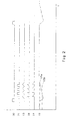
- Falls below the output voltage (15) to be regulated has a predefined lower value (15b), starts the oscillation, and the output (8) of the Schmitt trigger inverter generates voltage pulses with which the first switch (19) of the Voltage converter is switched on and off and current pulses are generated.
- the loading process of the Storage capacitor (20) can also refer to a single threshold to be controlled. In the case described above, the upper value would then be (15a) equal to the lower value (15b).
- the generated by the pulse controller Voltage pulses switch the first switch of the voltage booster for a first predefined time period and for a second predefined one Period of time.
- the first predefined time period determines the current strength of the Current pulses (13) through the inductor (16)
- the first predefined time period of the voltage pulses generated by the pulse regulator is of the amount of supplied output voltage of the voltage step-up affected, since the Switching point of the Schmitt trigger inverter by the supplied voltage is moved. This advantageously achieves additional regulation Pulse width modulation in the range of small deviations from the predefined Target value (15a) of the output voltage.
- the Zener tension of the Zener diode (5) becomes the setpoint of the output voltage to be regulated Voltage step-up specified.
- a combination through series connection of several Zener diodes allows voltage setpoints to be specified by Single zener diodes are not covered.
- the diode (6) prevents the Switch on the operating voltage of the voltage step-up and pulse regulator the Zener diode continues to conduct and the Schmitt trigger inverter the first
- the voltage boost switch keeps on.
- Other Embodiments of a pulse regulator, the output voltage to be controlled of the voltage step-up converter in control voltage pulses to control the implement the first switch are possible.
- An embodiment in Fig. 1 of an output switch (3) according to the Claims 12 to 15 consists of a first load switch (23), designed as P-channel MOSFET transistor or PNP bipolar transistor, a second Load switch (29), designed as an N-channel MOSFET transistor or NPN bipolar transistor, a first diode for energy return (24), a second diode for energy return (26), a Zener diode (22) and a resistor (25).
- the first switching connection of the first load switch is with the output voltage (15) of the voltage step-up converter (2) connected, the second switching connection of the The first load switch is connected to a first connection (31) of the ultrasound excitation circuit (4) connected, alternatively as an inductor (32) and Resistor (33) is shown.
- the first switching connection of the second The load switch (29) is connected to the second connection (34) of the ultrasound excitation circuit connected, the second switching connection of the second The load switch is connected to the reference potential.
- the cathode of the first Diode (24) is with the output voltage of the voltage step-up connected, the anode of the first diode is connected to the second terminal of the Ultrasonic excitation circuit connected.
- the cathode of the second diode (26) is connected to the first connection (31) of the ultrasound excitation circuit, the anode of the second diode is at the common reference potential connected.
- Zener diode (22) The cathode of the Zener diode (22) is with the output voltage of the Voltage booster connected, its anode is connected to the gate of the P-channel MOSFET transistor and through a resistor to the drain Connection of the N-channel MOSFET transistor connected. Via Zener Diode (22) and resistor (25) becomes the P-channel MOSFET transistor by turning on of the N-channel MOSFET transistor switched on, so that to generate a Current pulse in the ultrasonic excitation circuit both load switches simultaneously are switched on and on the storage capacitor of the voltage booster applied voltage is supplied to the ultrasonic excitation circuit.
- the Gate connection of the N-channel MOSFET transistor (29) is a signal for Generation of current pulses (30) in the ultrasound excitation circuit, that is generated by a control unit not described here.
- the diodes (24, 26) lead after switching off the switches (23, 29) Self-induction energy from the ultrasound excitation circuit as a current pulse back into the storage capacitor (20).
- An embodiment in Fig. 5 of an output switch without Energy recirculation (4) according to claims 16 to 18 consists of a Load switch (29) and a diode (46).
- a first connection (31) of the ultrasound excitation circuit (4) is with the output voltage of the step-up converter connected.
- the first switching connection of the load switch (29) is with connected to the second connection (34) of the ultrasound excitation circuit second switching connection of the load switch is with the reference potential (11) connected.
- the cathode of the diode (46) is connected to the first connection of the Ultrasonic excitation circuit connected, the anode of the diode is connected to the second connection of the ultrasonic excitation circuit connected.
- the diode takes the self-induction energy of the ultrasonic excitation circuit as a freewheeling diode while avoiding high voltage pulses when Turn off on.
- the advantages of the invention are based on the fact that a pulse output voltage is generated by the Zener voltage of the Zener diode in any Ratio greater than or equal to the input voltage is specified. Another The advantage is that with switched charging current pulses the linear control resulting power loss is avoided.
- the use of a standard logic circuit like 74HC14 in single logic gate design allows one particularly cost-effective and space-saving construction.
Landscapes
- Engineering & Computer Science (AREA)
- Power Engineering (AREA)
- Dc-Dc Converters (AREA)
- Length Measuring Devices Characterised By Use Of Acoustic Means (AREA)
- Ultra Sonic Daignosis Equipment (AREA)
- Investigating Or Analyzing Materials By The Use Of Ultrasonic Waves (AREA)
Description
Claims (15)
- Ultraschall-Positionssensor mit einem Impulsgenerator mit hohem Wirkungsgrad zur Erzeugung von kurzen Spannungsimpulsen, umfassendeinen Spannungshochsetzer (2), der einen ersten Schalter (19; 43), einem zweiten Schalter (17), eine Induktivität (16; 45) und einen Speicherkondensator (20) aufweist, wobei der erste Schalter (19;43) Strompulse in der Induktivität (16; 45) erzeugt, die dem Speicherkondensator (20) zugeführt werden, wenn ein unterer Grenzwert (15b) einer Ausgangsspannung (15) unterschritten ist,einen Impulsregler (1), der den ersten Schalter (19) ansteuert, bis die Ausgangsspannung (15) einen oberen Grenzwert (15a) erreicht hat, der größer oder gleich dem unteren Grenzwert (15b) sein kann, wobei der Impulsregler (1) einen steuerbaren Impulserzeuger mit einem Schmitt-Trigger-Inverter (10), einen Schwingkreiskondensator (9) und einen Widerstand (7) umfaßt, dessen Ausgangsimpulse durch eine von der Ausgangsspannung (15) über eine Zenerdiode (5) abgeleitete Teilspannung beeinflußt werden, wobei die Zenerspannung den Arbeitsbereich des Impulserzeugers festlegt,einen Ultraschall-Erregerstromkreis (4), undeinen ausgangsseitigen Schalter (3) mit einem Lastschalter (23, 29), der zur Erzeugung eines Spannungsimpulses in dem Ultraschall-Erregerstromkreis (4) eingeschaltet wird, wodurch die an dem Speicherkondensator (20) anliegende Spannung dem Ultraschall-Erregerstromkreis (4) so lange zugeführt wird, bis der untere Grenzwert (15b) der Ausgangsspannung (15) unterschritten ist.
- Impulsgenerator nach Anspruch 1,
dadurch gekennzeichnet, daß
der Spannungs-Hochsetzer (2) einen zweiten Schalter (17) aufweist, der zwischen der Induktivität (16) und dem Speicherkondehsator (20) zwischengeschaltet ist. - Impulsgenerator nach Anspruch 2,
dadurch gekennzeichnet, daß
der zweite Schalter eine Diode ist. - Impulsgenerator nach Anspruch 1,
dadurch gekennzeichnet, daß
der erste Schalter (19) ein MOS- oder Bipolar-Transistor ist. - Impulsgenerator nach einem der vorhergehenden Ansprüche 1 bis 4,
dadurch gekennzeichnet, daß
ein erster Anschluß der Induktivität (16) an einer Eingangsspannung liegt, ein zweiter Anschluß der Induktivität (16) mit einem ersten Anschluß des ersten Schalters (19) und mit einem ersten Anschluß des zweiten Schalters (17) verbunden ist, der Steueranschluß des ersten Schalters (19) mit dem Ausgang des Impulsreglers (1), ein zweiter Anschluß des zweiten Schalters (17) mit einem ersten Anschluß des Speicherkondensators (20) verbunden ist, und ein zweiter Anschluß des Speicherkondensators (20) und ein zweiter Schaltanschluß des ersten Schalters mit dem Bezugspotential verbunden sind. - Impulsgenerator nach einem der Ansprüche 1 bis 5,
dadurch gekennzeichnet, daß
der Impulsregler (1) eine Zenerdiode (5), eine Diode (6), einen Schmitt-Trigger-Inverter (10), einen Schwingkreiskondensator (9) und einen Widerstand (7) aufweist, wobei die Kathode der Zenerdiode (5) mit der Ausgangsspannung (15) des Spannungs-Hochsetzers (2), die Anode der Zenerdiode (5) mit der Anode der Diode (6), die Kathode der Diode (6) mit dem Eingang des Schmitt-Trigger-Inverters (10), der erste Anschluß des Schwingkreiskondensators (9) mit dem Eingang des Schmitt-Trigger-Inverters (10), der zweite Anschluß des Schwingkreiskondensators (9) mit dem Bezugspotential (11), der erste Anschluß des Widerstands (7) mit dem Eingang des Schmitt-Trigger-Inverters (10), der zweite Anschluß des Widerstandes (7) mit dem Ausgang des Schmitt-Trigger-Inverters (10), und der Ausgang des Schmitt-Trigger-Inverters (10) mit dem Steuereingang des ersten Schalters (19) des Spannungs-Hochsetzers (2) verbunden ist, und der Schmitt-Trigger-Inverter (10) mit einer Versorgungsspannung zwischen 1V und 15V versorgt wird. - Impulsgenerator nach Anspruch 1,
dadurch gekennzeichnet, daß
ein ausgangsseitiger Schalter mit Ehergierückführung (3) mit einem ersten Lastschalter (23), einem zweiten Lastschalter (29), einer ersten Diode (24) und einer zweiten Diode (26) vorgesehen ist. - Impulsgenerator nach Anspruch 7,
dadurch gekennzeichnet, daß
ein erster Anschluß des ersten Lastschalters (23) mit der Ausgangsspannung (15) des Spannungs-Hochsetzers (2), ein zweiter Anschluß des ersten Lastschalters (23) mit einem ersten Anschluß eines Lastelementes (4), ein erster Anschluß des zweiten Lastschalters (29) mit einem zweiten Anschluß des Lastelementes(4), ein zweiter Anschluß des zweiten Lastschalters (29) mit dem Bezugspotential (11), die Kathode der ersten Diode (24) mit der Ausgangsspannung (15) des Spannungs-Hochsetzers (2) die Anode der ersten Diode (24) mit dem zweiten Anschluß des Lastelementes (4), die Kathode der zweiten Diode (26) mit dem ersten Anschluß des Lastelementes (4), und die Anode der zweiten Diode (26) mit dem gemeinsamen Bezugspotential (11), verbunden ist, und zum Erzeugen eines Stromimpulses im Lastelement (4) beide Lastschalter (23, 29) gleichzeitig ein- und ausgeschaltet werden. - Impulsgenerator nach Anspruch 8,
dadurch gekennzeichnet, daß
der erste Lastschalter (23) ein P-Kanal MOS-Transistor, und der zweite Lastschalter (29) ein N-Kanal MOS-Transistor ist, und eine Zenerdiode (22) vorgesehen ist, deren Kathode mit der Ausgangsspannung (15) und deren Anode mit dem Gate-Anschluß des P-Kanals MOS-Transistors und über einen Widerstand (25) mit dem Drain-Anschluß des N-Kanal MOS-Transistors verbunden ist. - Impulsgenerator nach Anspruch 8,
dadurch gekennzeichnet, daß
der erste Lastschalter (23) ein PNP-Bipolar-Transistor und der zweite Lastschalter (29) ein NPN-Bipolar-Transistor ist, und eine Zenerdiode (22) vorgesehen ist, deren Kathode mit der Ausgangsspannung (15) des Spannungs-Hochsetzers (2), und deren Anode mit dem Basis-Anschluß des PNP-Bipolar-Transistors und über einen Widerstand mit dem Kollektor-Anschluß des NPN-Bipolar-Transistors verbunden ist. - Impulsgenerator nach Anspruch 1,
dadurch gekennzeichnet, daß
ein ausgangsseitiger Schalter ohne Energierückführung (3), mit einem Lastschalter und einer Diode (46) vorgesehen ist. - Impulsgenerator nach Anspruch 11,
dadurch gekennzeichnet, daß
der erste Anschluß des Lastelementes (4) mit der Ausgangsspannung (15) des Spannungs-Hochsetzers (2), der erste Schaltanschluß des Lastschalters (29) mit dem zweiten Anschluß des Lastelementes (4), der zweite Schaltanschluß des Lastschalters (29) mit dem Bezugspotential (11), die Kathode der Diode (46) mit dem ersten Anschluß des Lastelementes (4), und die Anode der Diode (46) mit dem zweiten Anschluß des Lastelementes (4) verbunden ist. - Impulsgenerator nach Anspruch 1,
dadurch gekennzeichnet, daß
der erste und/oder zweite Lastschalter (23, 29) ein MOS- oder Bipolar-Transistor ist. - Impulsgenerator nach Anspruch 12,
dadurch gekennzeichnet, daß
zwischen dem zweiten Anschluß des Lastelementes (4) und dem zweiten Schalter (29) ein Widerstand (28) eingefügt ist. - Impulsgenerator nach Anspruch 1,
dadurch gekennzeichnet, daß
der erste Anschluß des ersten Schalters (43) mit der Eingangsspannung, der zweite Anschluß des ersten Schalters (43) mit dem ersten Anschluß der Induktivität (45) und der Kathode der Diode (44), der Steueranschluß des ersten Schalters (43) mit dem Ausgang des Impulsreglers (1), der zweite Anschluß der Induktivität (45) mit dem Bezugspotential (11), und die Anode der Diode (44) mit dem ersten Anschluß des Speicherkondensators (20) verbunden ist.
Applications Claiming Priority (3)
| Application Number | Priority Date | Filing Date | Title |
|---|---|---|---|
| DE19714980A DE19714980C2 (de) | 1997-04-10 | 1997-04-10 | Ultraschall-Positionssensor mit einem Impulsgenerator zur Erzeugung von kurzen Spannungsimpulsen |
| DE19714980 | 1997-04-10 | ||
| PCT/EP1998/002108 WO1998045932A1 (de) | 1997-04-10 | 1998-04-09 | Impulsgenerator mit hohem wirkungsgrad zur erzeugung von kurzen spannungsimpulsen |
Publications (2)
| Publication Number | Publication Date |
|---|---|
| EP0974187A1 EP0974187A1 (de) | 2000-01-26 |
| EP0974187B1 true EP0974187B1 (de) | 2001-08-29 |
Family
ID=7826116
Family Applications (1)
| Application Number | Title | Priority Date | Filing Date |
|---|---|---|---|
| EP98920510A Expired - Lifetime EP0974187B1 (de) | 1997-04-10 | 1998-04-09 | Impulsgenerator mit hohem wirkungsgrad zur erzeugung von kurzen spannungsimpulsen |
Country Status (5)
| Country | Link |
|---|---|
| US (1) | US6680603B1 (de) |
| EP (1) | EP0974187B1 (de) |
| DE (2) | DE19714980C2 (de) |
| ES (1) | ES2165160T3 (de) |
| WO (1) | WO1998045932A1 (de) |
Families Citing this family (15)
| Publication number | Priority date | Publication date | Assignee | Title |
|---|---|---|---|---|
| US6051744A (en) * | 1998-12-17 | 2000-04-18 | Chevron Chemical Company Llc | Low pressure hydrodealkylation of ethylbenzene and xylene isomerization |
| US6903535B2 (en) * | 2002-04-16 | 2005-06-07 | Arques Technology, Inc. | Biasing system and method for low voltage DC—DC converters with built-in N-FETs |
| US6809503B1 (en) * | 2003-01-13 | 2004-10-26 | Linear Technology Corporation | Systems and methods for conserving energy in a switching circuit |
| DE102004060577B4 (de) * | 2004-12-16 | 2010-08-12 | Fraunhofer-Gesellschaft zur Förderung der angewandten Forschung e.V. | Schaltung und Verfahren zum Erzeugen eines Strompulses in einem Wellenleiter |
| US7898148B2 (en) * | 2005-09-30 | 2011-03-01 | Nxp B.V. | Oscillator based on piezoresistive resonators |
| US8427137B2 (en) | 2007-12-14 | 2013-04-23 | Mts Systems Corporation | Magnetostrictive displacement transducer with suppression of switching power supply noise |
| US8054066B2 (en) | 2007-12-14 | 2011-11-08 | Mts Systems Corporation | Magnetostrictive displacement transducer with phase shifted bias burst |
| KR101942028B1 (ko) * | 2011-09-22 | 2019-01-25 | 삼성전자 주식회사 | Led 조명 장치 |
| US9088207B2 (en) | 2012-06-04 | 2015-07-21 | Stangenes Industries, Inc. | Long pulse droop compensator |
| US8963617B1 (en) * | 2013-09-20 | 2015-02-24 | Linear Technology Corporation | Switching topology for connecting two nodes in electronic system |
| JP6446340B2 (ja) * | 2015-08-24 | 2018-12-26 | 本田技研工業株式会社 | 電磁デバイス駆動装置及び車両 |
| US10212799B2 (en) * | 2016-02-15 | 2019-02-19 | Stangenes Industries, Inc. | System and method for high power pulse generator |
| JP7056146B2 (ja) * | 2017-12-27 | 2022-04-19 | セイコーエプソン株式会社 | 超音波測定装置、及び測定方法 |
| JP7548408B2 (ja) * | 2021-03-03 | 2024-09-10 | 株式会社村田製作所 | 物体検知システム |
| JPWO2023013285A1 (de) * | 2021-08-04 | 2023-02-09 |
Family Cites Families (28)
| Publication number | Priority date | Publication date | Assignee | Title |
|---|---|---|---|---|
| DE295446C (de) | ||||
| US3571697A (en) * | 1968-12-16 | 1971-03-23 | Collins Radio Co | Variable impedance switching regulator |
| US3974439A (en) * | 1975-03-05 | 1976-08-10 | Texas Instruments Incorporated | Wide dynamic current range switching regulator |
| US4155112A (en) * | 1977-06-06 | 1979-05-15 | Motorola, Inc. | Power supply circuitry |
| US4434402A (en) | 1980-08-23 | 1984-02-28 | Smiths Industries Public Limited Company | Electrical equipment |
| JPS5791023A (en) | 1980-11-26 | 1982-06-07 | Mitsubishi Electric Corp | Pulse current generator |
| DE3131455A1 (de) | 1981-08-08 | 1983-03-24 | Gebhard Balluff GmbH & Co Feinmechanische Erzeugnisse, 7303 Neuhausen | Magnetostriktiver wegmesser |
| US4473875A (en) * | 1982-01-21 | 1984-09-25 | The United States Of America As Represented By The United States Department Of Energy | Inductive storage pulse circuit device |
| FR2538942B1 (fr) * | 1982-12-29 | 1989-05-05 | Renault | Dispositif de commande d'organe(s) electromagnetique(s) a actionnement rapide, tel(s) qu'electrovanne(s) ou injecteur(s) |
| US4549254A (en) * | 1983-02-03 | 1985-10-22 | Chrysler Corporation | Buck-boost regulated D.C. to D.C. power supply |
| DK232783D0 (da) | 1983-05-24 | 1983-05-24 | Radiometer As | Elektrokemisk maleelektrodeindretning og fremgangsmade til transmission af signaler fra samme |
| JPS605620A (ja) | 1983-06-23 | 1985-01-12 | Mitsubishi Electric Corp | 電源装置 |
| DE3627395A1 (de) * | 1986-08-13 | 1988-02-18 | Patent Treuhand Ges Fuer Elektrische Gluehlampen Mbh | Steuerschaltung fuer ein schaltnetzteil mit sinusfoermiger stromaufnahme zum umwandeln einer sinusfoermigen wechselspannung in eine geregelte gleichspannung |
| US4683529A (en) * | 1986-11-12 | 1987-07-28 | Zytec Corporation | Switching power supply with automatic power factor correction |
| CA1295670C (en) * | 1987-12-11 | 1992-02-11 | Tooru Kido | Dc supply having low and high constant voltages for powering an inverter controller |
| DE4005129A1 (de) * | 1990-02-17 | 1991-08-22 | Degussa | Vorrichtung zur induktiven erwaermung von koerpern mittels hochfrequenter schwingungen |
| EP0448908B1 (de) * | 1990-03-27 | 1994-12-14 | Saia Ag | Verfahren zur Erzeugung einer stabilen Gleichspannung und stabile Gleichspannungsquelle |
| FR2667357A1 (fr) * | 1990-09-28 | 1992-04-03 | Renault | Dispositif de commande d'injecteurs de combustible dans un moteur a combustion interne. |
| DD295446A5 (de) * | 1990-10-02 | 1991-10-31 | Akademie Der Wissenschaften Der Ddr Zentrum Fuer Wissenschaftlichen Geraetebau,De | Hochspannungsimpulsgenerator fuer impulsgaslaser |
| WO1992015844A1 (en) | 1991-03-11 | 1992-09-17 | Mts Systems Corporation | Emulated encoder output magnetostrictive position transducer |
| JP2582749Y2 (ja) * | 1992-10-01 | 1998-10-08 | アスコ株式会社 | スイッチング昇圧回路 |
| JP3294343B2 (ja) * | 1992-11-13 | 2002-06-24 | 松下電工株式会社 | 電源装置 |
| US5587680A (en) | 1995-06-30 | 1996-12-24 | Mts Systems Corporation | Pulse generator with charge pump |
| US5610502A (en) * | 1995-08-24 | 1997-03-11 | Delco Electronics Corp. | Boost power supply with clock period compensation |
| US5757166A (en) * | 1995-11-30 | 1998-05-26 | Motorola, Inc. | Power factor correction controlled boost converter with an improved zero current detection circuit for operation under high input voltage conditions |
| WO1997023765A1 (en) | 1995-12-22 | 1997-07-03 | A/S Brüel & Kjær | A system and a method for measuring a continuous signal |
| DE19548629C1 (de) * | 1995-12-23 | 1997-07-24 | Itt Ind Gmbh Deutsche | Komplementäres Taktsystem |
| US6232752B1 (en) * | 1999-11-10 | 2001-05-15 | Stephen R. Bissell | DC/DC converter with synchronous switching regulation |
-
1997
- 1997-04-10 DE DE19714980A patent/DE19714980C2/de not_active Expired - Fee Related
-
1998
- 1998-04-09 WO PCT/EP1998/002108 patent/WO1998045932A1/de not_active Ceased
- 1998-04-09 EP EP98920510A patent/EP0974187B1/de not_active Expired - Lifetime
- 1998-04-09 DE DE59801320T patent/DE59801320D1/de not_active Expired - Lifetime
- 1998-04-09 ES ES98920510T patent/ES2165160T3/es not_active Expired - Lifetime
-
1999
- 1999-10-12 US US09/416,538 patent/US6680603B1/en not_active Expired - Lifetime
Also Published As
| Publication number | Publication date |
|---|---|
| EP0974187A1 (de) | 2000-01-26 |
| WO1998045932A1 (de) | 1998-10-15 |
| DE59801320D1 (de) | 2001-10-04 |
| DE19714980A1 (de) | 1998-10-15 |
| US6680603B1 (en) | 2004-01-20 |
| ES2165160T3 (es) | 2002-03-01 |
| DE19714980C2 (de) | 2001-01-04 |
Similar Documents
| Publication | Publication Date | Title |
|---|---|---|
| DE60101991T2 (de) | Gleichstrom zu Gleichstrom-Umwandler | |
| DE2600890C3 (de) | Ultraschallgenerator mit einem Ultraschallwandler | |
| DE19714980C2 (de) | Ultraschall-Positionssensor mit einem Impulsgenerator zur Erzeugung von kurzen Spannungsimpulsen | |
| EP0609875B1 (de) | Verfahren zum Begrenzen der Frequenz eines spannungsgesteuerten Oszillators in einer Steuerschaltung eines Resonanzwandler-Schaltnetzteils und Steuerschaltung für ein Resonanzwandler-Schaltnetzteil | |
| DE3785534T2 (de) | Parallel resonanter auf-abwaertskonverter. | |
| EP0705482B1 (de) | Schaltungsanordnung zur ansteuerung eines schützes | |
| EP0380033B1 (de) | Schaltungsanordnung für ein freischwingendes Sperrwandler-Schaltnetzteil | |
| DE102009045052B4 (de) | Bereitstellen einer Versorgungsspannung für eine Ansteuerschaltung eines Halbleiterschaltelements | |
| DE10016859A1 (de) | Schalt-Energieversorgung mit einer Niederenergie-Burstbetriebsart | |
| DE2255822B2 (de) | Treiberschaltung für eine lichtemittierende Diode | |
| DE102006014276B4 (de) | Elektromagnetventil und Elektromagnetventil-Antriebsschaltung | |
| EP0419724A1 (de) | Schaltungsanordnung für ein Sperrwandler-Schalnetzteil | |
| DE4236067A1 (de) | Hochfrequenzinduktionsheizvorrichtung | |
| DE4406546B4 (de) | Treiberschaltung eines schaltbaren Reluktanzmotors | |
| EP0024300A1 (de) | Verfahren zur Pulsbreitensteuerung eines Gleichstrom-Umkehrstellers und Schaltungsanordnung zur Durchführung des Verfahrens | |
| DE2922309B2 (de) | Elektronischer Sensor-Ein/Aus-Schalter | |
| EP0664602B1 (de) | Sperrumrichter mit geregelter Ausgangsspannung | |
| DE69809128T2 (de) | Stromversorgungsvorrichtung | |
| DE2803847C2 (de) | Einrichtung zum drahtlosen Ferneinschalten und Fernausschalten von elektrischen Geräten | |
| EP0023622A1 (de) | Verfahren zur Pulsbreitensteuerung eines Gleichstrom-Umkehrstellers und Schaltungsanordnung zur Durchführung des Verfahrens | |
| DE2608167C3 (de) | Geregelter Eintakt-Durchflußumrichter zur Erzeugung mehrerer galvanisch getrennter Ausgangsspannungen | |
| DE3610156C2 (de) | ||
| EP0353533B1 (de) | Schaltungsanordnung bei Endstufen für die Steuerung von Stellmagneten | |
| DE2649306A1 (de) | Spannungsregler fuer generatoren in kraftfahrzeugen | |
| DE2952654A1 (de) | Gegentakt-wechselrichter |
Legal Events
| Date | Code | Title | Description |
|---|---|---|---|
| PUAI | Public reference made under article 153(3) epc to a published international application that has entered the european phase |
Free format text: ORIGINAL CODE: 0009012 |
|
| 17P | Request for examination filed |
Effective date: 19991109 |
|
| AK | Designated contracting states |
Kind code of ref document: A1 Designated state(s): DE ES FR GB IT |
|
| GRAG | Despatch of communication of intention to grant |
Free format text: ORIGINAL CODE: EPIDOS AGRA |
|
| GRAG | Despatch of communication of intention to grant |
Free format text: ORIGINAL CODE: EPIDOS AGRA |
|
| GRAH | Despatch of communication of intention to grant a patent |
Free format text: ORIGINAL CODE: EPIDOS IGRA |
|
| 17Q | First examination report despatched |
Effective date: 20001123 |
|
| GRAH | Despatch of communication of intention to grant a patent |
Free format text: ORIGINAL CODE: EPIDOS IGRA |
|
| GRAA | (expected) grant |
Free format text: ORIGINAL CODE: 0009210 |
|
| AK | Designated contracting states |
Kind code of ref document: B1 Designated state(s): DE ES FR GB IT |
|
| REF | Corresponds to: |
Ref document number: 59801320 Country of ref document: DE Date of ref document: 20011004 |
|
| REG | Reference to a national code |
Ref country code: GB Ref legal event code: IF02 |
|
| GBT | Gb: translation of ep patent filed (gb section 77(6)(a)/1977) |
Effective date: 20011130 |
|
| ET | Fr: translation filed | ||
| REG | Reference to a national code |
Ref country code: ES Ref legal event code: FG2A Ref document number: 2165160 Country of ref document: ES Kind code of ref document: T3 |
|
| PLBE | No opposition filed within time limit |
Free format text: ORIGINAL CODE: 0009261 |
|
| STAA | Information on the status of an ep patent application or granted ep patent |
Free format text: STATUS: NO OPPOSITION FILED WITHIN TIME LIMIT |
|
| 26N | No opposition filed | ||
| RIN2 | Information on inventor provided after grant (corrected) |
Free format text: STEINICH, KLAUS-MANFRED * WIRTH, PETER |
|
| PGFP | Annual fee paid to national office [announced via postgrant information from national office to epo] |
Ref country code: ES Payment date: 20070425 Year of fee payment: 10 |
|
| PGFP | Annual fee paid to national office [announced via postgrant information from national office to epo] |
Ref country code: GB Payment date: 20070425 Year of fee payment: 10 |
|
| PGFP | Annual fee paid to national office [announced via postgrant information from national office to epo] |
Ref country code: FR Payment date: 20070418 Year of fee payment: 10 |
|
| GBPC | Gb: european patent ceased through non-payment of renewal fee |
Effective date: 20080409 |
|
| REG | Reference to a national code |
Ref country code: FR Ref legal event code: ST Effective date: 20081231 |
|
| PG25 | Lapsed in a contracting state [announced via postgrant information from national office to epo] |
Ref country code: FR Free format text: LAPSE BECAUSE OF NON-PAYMENT OF DUE FEES Effective date: 20080430 |
|
| REG | Reference to a national code |
Ref country code: ES Ref legal event code: FD2A Effective date: 20080410 |
|
| PG25 | Lapsed in a contracting state [announced via postgrant information from national office to epo] |
Ref country code: GB Free format text: LAPSE BECAUSE OF NON-PAYMENT OF DUE FEES Effective date: 20080409 |
|
| PG25 | Lapsed in a contracting state [announced via postgrant information from national office to epo] |
Ref country code: ES Free format text: LAPSE BECAUSE OF NON-PAYMENT OF DUE FEES Effective date: 20080410 |
|
| REG | Reference to a national code |
Ref country code: DE Ref legal event code: R082 Ref document number: 59801320 Country of ref document: DE Representative=s name: WEICKMANN & WEICKMANN PATENT- UND RECHTSANWAEL, DE Ref country code: DE Ref legal event code: R082 Ref document number: 59801320 Country of ref document: DE Representative=s name: WEICKMANN & WEICKMANN PATENTANWAELTE - RECHTSA, DE Ref country code: DE Ref legal event code: R082 Ref document number: 59801320 Country of ref document: DE Representative=s name: PATENTANWAELTE WEICKMANN & WEICKMANN, DE |
|
| PGFP | Annual fee paid to national office [announced via postgrant information from national office to epo] |
Ref country code: IT Payment date: 20150423 Year of fee payment: 18 |
|
| PG25 | Lapsed in a contracting state [announced via postgrant information from national office to epo] |
Ref country code: IT Free format text: LAPSE BECAUSE OF NON-PAYMENT OF DUE FEES Effective date: 20160409 |
|
| PGFP | Annual fee paid to national office [announced via postgrant information from national office to epo] |
Ref country code: DE Payment date: 20170425 Year of fee payment: 20 |
|
| REG | Reference to a national code |
Ref country code: DE Ref legal event code: R071 Ref document number: 59801320 Country of ref document: DE |