EP0973093A2 - Méthode et appareil de traitement d'information, et support de présentation - Google Patents
Méthode et appareil de traitement d'information, et support de présentation Download PDFInfo
- Publication number
- EP0973093A2 EP0973093A2 EP99305033A EP99305033A EP0973093A2 EP 0973093 A2 EP0973093 A2 EP 0973093A2 EP 99305033 A EP99305033 A EP 99305033A EP 99305033 A EP99305033 A EP 99305033A EP 0973093 A2 EP0973093 A2 EP 0973093A2
- Authority
- EP
- European Patent Office
- Prior art keywords
- bus
- signal processing
- external device
- program
- processing means
- Prior art date
- Legal status (The legal status is an assumption and is not a legal conclusion. Google has not performed a legal analysis and makes no representation as to the accuracy of the status listed.)
- Withdrawn
Links
Images


Classifications
-
- G—PHYSICS
- G06—COMPUTING; CALCULATING OR COUNTING
- G06F—ELECTRIC DIGITAL DATA PROCESSING
- G06F9/00—Arrangements for program control, e.g. control units
- G06F9/06—Arrangements for program control, e.g. control units using stored programs, i.e. using an internal store of processing equipment to receive or retain programs
- G06F9/44—Arrangements for executing specific programs
- G06F9/4401—Bootstrapping
Definitions
- the present invention relates to a method of and an apparatus for processing information, and a providing medium.
- the memory device For designing a desired circuit with the DSPs mounted on the circuit board, however, the memory device needs to be of a large bit width configuration for transferring data at a high rate.
- the DSPs In order to be used with the memory device of a large bit width configuration, the DSPs are required to have a number of terminals, resulting in an increased DSP package size.
- a general-purpose memory device If a general-purpose memory device is to be used, then a plurality of such general-purpose memory devices because each one of the general-purpose memory devices has a small storage capacity.
- the circuit board is necessarily large in size, and interconnections between devices, e.g., interconnections between the memory device and the DSPs, are long, so that signal transfer delays will be caused by stray capacities on the circuit board. As a result, signals cannot be transferred efficiently at a high rate.
- the number of devices used increases, their power consumption and heat generation increase.
- the large-size circuit board tends to degrade itself soon.
- a bootstrap program for the graphic computers and video entertainment systems is fixedly stored in a built-in ROM. Therefore, even when a bug in the bootstrap program is found, it is difficult to eliminate the bug from the bootstrap program.
- Embodiments of the invention can provide a method of and an apparatus for transferring data efficiently at high speed, and a providing medium for providing a program and/or data to carry out such a method.
- Embodiments of the present invention can increase the signal processing capability of an apparatus such as a graphic computer or a video entertainment system, and allow a program in such an apparatus to be easily modified.
- FIG. 1 shows in block form a video entertainment system 1 which incorporates the principles of the present invention.
- the video entertainment system 1 has a host CPU (Central Processing Unit) 2 for controlling a media processor 4 according to a program which has been transferred from a recording medium 5 to a main memory 3 via a drive controller 14 and a host bus 22.
- a host CPU Central Processing Unit
- a bootstrap program is read from the recording medium 5 by the host CPU 2, which may be a CD-ROM (Compact Disk - Read-Only Memory), a DVD-ROM (Digital Video Disk - Read-Only Memory), or the like, into the main memory 3, and then transferred from the main memory 3 to the media processor 4, which may be regarded as an information processing apparatus, which then executes the bootstrap program.
- the main memory 3 comprises a RAM (Random-Access Memory), for example, and serves to store programs and data necessary to operate the host CPU 2.
- the recording medium 5 stores, in addition to the bootstrap program, application programs, audio signal data (including compressed data), video signal data (including compressed data), and other data.
- the media processor 4 After having executed the bootstrap program supplied via the host bus 22 by the host CPU 2, the media processor 4 reads an application program and necessary data supplied from the recording medium 5 via the main memory 3 by the host CPU 2. The media processor 4 also processes data to output an audio signal, processes a separately entered audio signal, and receives and outputs communication data for a modem or the like, according to the application program.
- a moving-image decoder 23 decodes compressed graphic data supplied from the main memory 3 and returns the decoded graphic data to the main memory 3, which stores the decoded graphic data.
- a graphic engine 24 processes the decoded graphic data, which has been supplied from the main memory 3 via the host bus 22, into a video signal, and outputs the video signal.
- the media processor 4 is regarded as an information processing apparatus, then the other components including the host CPU 2, the main memory 3, and the host bus 22 may be regarded as external devices.
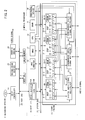
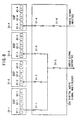
- FIG. 2 shows in block form the media processor 4, which comprises a single LSI circuit.
- a DRAM (Dynamic RAM) 11 stores the bootstrap program supplied by the host CPU 2 and also stores data required for the operation of and a program to be executed by a CPU 12, which functions also as a management means and a control means, and a sound engine 13.
- the CPU 12 executes various processing operations according to the program stored in the DRAM 11. For example, the CPU 12 executes an initializing process according to the bootstrap program transferred from the DRAM 11.
- a bus arbiter 15 serving as an arbitration means for arbitrating or providing the right to use a system bus 21.
- a host I/F (interface) 16 is connected to the host CPU 2 by the host bus 22 and is also connected to the system bus 21.
- the host I/F 16 comprises a reset register 16A and a FIFO (First-In, First-Out) memory 16B.
- DMA Direct Memory Access
- the DMA controller 17 acquires the right to use the system bus 21 through the bus arbiter 15, and transfers the program and data from the host CPU 2 via the FIFO memory 16B to the DRAM 11 according to a DMA transfer process.
- a peripheral device 18 comprises a timer for performing clock operation and an interrupt controller for generating interrupt pulses at preset periodic intervals.
- the sound engine 13 comprises four DSPs 31-1 through 31-4 (also collectively referred to as a "DSP 31") as an executing means for executing a certain process, a digital audio signal multiplexer 32, a synchronous serial signal multiplexer 33, and an asynchronous serial signal multiplexer 34.
- the DSP 31-1 comprises a digital audio signal I/F 41-1, a synchronous serial signal I/F 42-1, and an asynchronous serial signal 43-1, which are connected respectively to the digital audio signal multiplexer 32, the synchronous serial signal multiplexer 33, and the asynchronous serial signal multiplexer 34.
- the digital audio signal I/F 41-1 and the synchronous serial signal I/F 42-1 transfer data in synchronism with a clock signal.
- the asynchronous serial signal I/F 43-1 transfer data based on RS-232C.
- the DSP 31-1 is connected to the system bus 21 for reading a program and data from the DRAM 11 via the system bus 21 and storing the program and data in a built-in DRAM 44-1.
- the DSPs 31-2 through 31-4 are identical in structure to the DSP 31-1.
- the DSPs 31-2 through 31-4 comprise respective digital audio signal I/Fs 41-2 through 41-4, respective synchronous serial signal I/Fs 42-2 through 42-4, respective asynchronous serial signal I/Fs 43-2 through 43-4, and respective DRAMs 44-2 through 44-4.
- the DSPs 31-2 through 31-4 are corrected to the system bus 21, the digital audio signal multiplexer 32, the synchronous serial signal multiplexer 33, and the asynchronous serial signal multiplexer 34.
- the digital audio signal multiplexer 32 multiplexes digital audio signals supplied from the digital audio signal I/Fs 41-1 through 41-4 of the DSPs 31-1 through 31-4.
- the synchronous serial signal multiplexer 33 multiplexes digital audio signals supplied from the digital audio signal I/Fs 42-1 through 42-4 of the DSPs 31-1 through 31-4.
- the asynchronous serial signal multiplexer 34 multiplexes digital audio signals supplied from the digital audio signal I/Fs 43-1 through 43-4 of the DSPs 31-1 through 31-4.
- the multiplexers 32, 33, 34 also serve as transfer means for transferring data in bypassing relation to the system bus 21.
- the media processor 4 is fabricated as one semiconductor device (LSI circuit) for thereby allowing the system bus 21 to have a large bit width (128 bits in the illustrated embodiment). Since the delay in accessing the DRAM 11 is small, data can be transferred between the DRAM 11 and the CPU 12, the DSPs 31-1 through 31-4 at a high rate and hence frequently. Therefore, the DRAMs 44-1 through 44-4 of the DSPs 31-1 through 31-4 may be of a relatively small storage capacity.
- the host CPU 2 supplies the media processor 4 with a reset signal (e.g., a signal having a low level) via a dedicated reset line (not shown) in step S1.
- a reset signal e.g., a signal having a low level
- the resources in the media processor 4, i.e., the CPU 12, the DSPs 31, the bus arbiter 15, etc. are reset by the reset signal.
- the reset register 16A of the host I/F 16, which manages reset states of the CPU 12 and the DSPs 31, is turned on (reset).
- step S2 When the host CPU 2 disables the reset signal, i.e., changes the reset signal from the low level to the high level, in step S2, the CPU 12 and the DSPs 31 (accurately their cores) remain reset (the reset register 16A remains turned on), but the other resources, e.g., the bus arbiter 15 and the DMA controller 17, are released from their reset states. Then, the host CPU 2 requests the bus arbiter 15 for the right to use the system bus 21 via the host I/F 16. The CPU 12 and the DSPs 31 do not request the bus arbiter 15 for the right to use the system bus 21 because they are still being reset. Therefore, the bus arbiter 15 gives the host CPU 2 the right to use the system bus 21 in step S3.
- the bus arbiter 15 gives the host CPU 2 the right to use the system bus 21 in step S3.
- step S4 the host CPU 2 initializes the DMA controller 17, the peripheral device 18, etc.
- step S5 the host CPU 2 instructs the CPU 12 to transfer the bootstrap program stored in the main memory 3.
- the bus arbiter 15 gives the DMA controller 17 the right to use the system bus 21 in step S6.
- step S7 the DMA controller 17 effects a DMA transfer of the bootstrap program from the main memory 3 via the system bus 21 to the DRAM 11.
- step S8 the host CPU 2 turns off the reset register 16A of the host I/F 16, i.e., releases the reset register 16A from its reset state.
- the CPU 12 and the DSPs 31 are now released from their reset states.
- the bus arbiter 15 gives the CPU 12 the right to use the system bus 21 in step S9.
- the CPU 12 receives the bootstrap program transferred from the DRAM 11, and executes an initializing process.
- the CPU 12 also controls the DSPs 31 to execute an initializing process.
- each of the DSPs 31-1 through 31-4 requests the bus arbiter 15 for the right to use the system bus 21.
- each of the DSPs 31-1 through 31-4 receives the bootstrap program transferred from the DRAM 11, and executes an initializing process.
- the host CPU 2 may control the DSPs 31 to execute an initializing process, rather than having the CPU 12 control the DSPs 31 to execute an initializing process.
- the bootstrap program can be modified when necessary. Consequently, when a bug is found in the bootstrap program, the bootstrap program may be improved, and the improved bootstrap program may be stored in the main memory 3. Other programs may similarly be debugged and stored.
- the host CPU 2 Because the host CPU 2 is able to obtain the right to use the system bus 21, the host CPU 2 can use resources of the media processor 4 and know their states. Accordingly, the debugging process is facilitated when a program is developed.
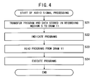
- step S21 the host CPU 2 controls the drive controller 14 to read programs and necessary data from the recording medium 5 and supply them to the FIFO memory 16B, which stores the supplied program and data.
- the DMA controller 17 then transfers the data stored in the FIFO memory 16B to the DRAM 11 according to a DMA transfer process.
- step S22 the CPU 12 indicates programs to be executed to the DSPs 31-1 through 31-4.
- step S23 the DSPs 31-1 through 31-4 request the bus arbiter 15 for the right to use the system bus 21.
- the DSPs 31-1 through 31-4 are given the right to use the system bus 21, the DSPs 31-1 through 31-4 read desired programs from the DRAM 11 and store them in the respective built-in DRAMs 44-1 through 44-4 in step S23.
- step S24 the DSPs 31-1 through 31-4 execute the programs stored in the DRAMs 44-1 through 44-4.
- the DSPs 31-1 through 31-4 execute a speech synthesis process, a sound synthesis process, a speech recognition process, and a sound effect process.
- the DSPs 31-1 through 31-4 read data necessary to execute the programs directly from the DRAM 11, but not via the CPU 12.
- the DSPs 31-1 through 31-4 read programs recorded in the recording medium 5 to process audio signals.
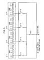
- the digital audio signal multiplexer 32 shown in FIGS. 5 through 8 comprises five switches 51-1 through 51-5.
- the switches 51-1 through 51-5 have respective terminals connected to the digital audio signal I/Fs 41-1 through 41-4 of the DSPs 31-1 through 31-4, respectively, and respective other terminals connected in common to a terminal of a switch 51-5.
- the other terminal of the switch 51-5 is connected to an external unit such as a speaker or a microphone (not shown).
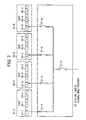
- FIG. 8 shows a modified digital audio signal multiplexer 32A that can be incorporated in the sound engine 13.
- the modified digital audio signal multiplexer 32A comprises six switches 51-1 through 51-6.
- the switches 51-1 through 51-3 have respective terminals connected to the digital audio signal I/Fs 41-1 through 41-3 of the DSPs 31-1 through 31-3, respectively, and respective other terminals connected in common to a terminal of a switch 51-5.
- the other terminal of the switch 51-5 is connected to an external unit such as a speaker or a microphone (not shown).
- the switch 51-4 has a terminal connected to the digital audio signal I/F 41-4 of the DSP 31-4 and the other terminal to an external unit such as a speaker or a microphone (not shown).
- the DSPs 31-1 through 31-4 are in an audio signal output mode, and the switches 51-1, 51-5 are turned on and the switches 51-2 through 51-4 are turned off. With these DSP and switch settings, an audio signal outputted from the DSP 31-1 is outputted via the switch 51-5 to the external unit. Therefore, in the mode of operation shown in FIG. 5, an audio signal outputted from either one of the DSPs 31-1 through 31-4 can be selected and outputted to the external unit.
- the DSPs 31-1 through 31-4 are in an audio signal input mode, and the switches 51-1, 51-2, 51-5 are turned on and the switches 51-3, 51-4 are turned off. With these DSP and switch settings, an audio signal inputted from the external unit is applied to the DSPs 31-1, 31-2. Therefore, in the mode of operation shown in FIG. 6, an audio signal inputted from the external unit can be inputted to one or more of the DSPs 31-1 through 31-4.
- the DSP 31-1 is in an audio signal output mode, and the DSPs 31-2, 31-3 are in an audio signal input mode.
- the switches 51-1 through 51-3 are turned on, and the switches 51-4, 51-5 are turned off.
- an audio signal outputted from the DSP 31-1 is supplied to the DSPs 31-2, 31-3. Accordingly, data can be transferred between the DSPs 31-1 through 31-4 in bypassing relation to the system bus 21.
- the DSP 31-1 is in an audio signal output mode, and the DSPs 31-2, 31-3, 31-4 are in an audio signal input mode.
- the switches 51-1 through 51-6 are turned on. With these DSP and switch settings, an audio signal outputted from the DSP 31-1 is supplied to the DSPs 31-2, 31-3, and outputted via the switch 51-5 to the external unit connected thereto. Furthermore, an audio signal outputted from the external unit connected to the switch 51-6 is supplied to the DSP 31-4 via the switches 51-6, 51-4.
- the synchronous serial signal multiplexer 33 and the asynchronous serial signal multiplexer 34 are basically identical in structure to the digital audio signal multiplexer 32 or digital audio signal multiplexer 32A. Therefore, the synchronous serial signal multiplexer 33 and the asynchronous serial signal multiplexer 34 can process synchronous and asynchronous serial signals, respectively, in the manner described above with reference to FIGS. 5 through 8.
- system represents an overall arrangement made up of a plurality of units, devices, means, or individual components.
- a providing medium for providing a computer program and/or data which carries out the above processing to the user may comprise any of various information recording mediums including a magnetic disk, an optical disk such as a CD-ROM, a solid-state memory, etc., and any of various information transmission mediums used in networks and satellite systems, etc.
- the programs can easily be modified.
- the data can be transferred efficiently at a high rate.
Landscapes
- Engineering & Computer Science (AREA)
- Software Systems (AREA)
- Theoretical Computer Science (AREA)
- Computer Security & Cryptography (AREA)
- Physics & Mathematics (AREA)
- General Engineering & Computer Science (AREA)
- General Physics & Mathematics (AREA)
- Bus Control (AREA)
- Reverberation, Karaoke And Other Acoustics (AREA)
Applications Claiming Priority (2)
| Application Number | Priority Date | Filing Date | Title |
|---|---|---|---|
| JP10180014A JP2000010913A (ja) | 1998-06-26 | 1998-06-26 | 情報処理装置および方法、並びに提供媒体 |
| JP18001498 | 1998-06-26 |
Publications (2)
| Publication Number | Publication Date |
|---|---|
| EP0973093A2 true EP0973093A2 (fr) | 2000-01-19 |
| EP0973093A3 EP0973093A3 (fr) | 2005-11-23 |
Family
ID=16075959
Family Applications (1)
| Application Number | Title | Priority Date | Filing Date |
|---|---|---|---|
| EP99305033A Withdrawn EP0973093A3 (fr) | 1998-06-26 | 1999-06-25 | Méthode et appareil de traitement d'information, et support de présentation |
Country Status (3)
| Country | Link |
|---|---|
| US (1) | US6427181B1 (fr) |
| EP (1) | EP0973093A3 (fr) |
| JP (1) | JP2000010913A (fr) |
Families Citing this family (13)
| Publication number | Priority date | Publication date | Assignee | Title |
|---|---|---|---|---|
| US6807620B1 (en) * | 2000-02-11 | 2004-10-19 | Sony Computer Entertainment Inc. | Game system with graphics processor |
| US6609188B1 (en) * | 2000-03-31 | 2003-08-19 | Intel Corporation | Data flow processor |
| US7093104B2 (en) | 2001-03-22 | 2006-08-15 | Sony Computer Entertainment Inc. | Processing modules for computer architecture for broadband networks |
| JP2004199187A (ja) * | 2002-12-16 | 2004-07-15 | Matsushita Electric Ind Co Ltd | Cpu内蔵lsi |
| CN1324495C (zh) * | 2003-08-28 | 2007-07-04 | 北京鼎视通软件技术有限公司 | 一种基于多媒体处理器的图形处理方法 |
| US8219226B2 (en) | 2007-09-01 | 2012-07-10 | D2Audio Corporation | Systems and methods for overriding hardwired responses in an HDA codec |
| WO2009029919A1 (fr) * | 2007-09-01 | 2009-03-05 | D2Audio Corporation | Systèmes et procédés pour masquer un codec hda |
| TW200913471A (en) | 2007-09-01 | 2009-03-16 | D2Audio Corp | Systems and methods for controlling HDA system capabilities |
| US8224469B2 (en) | 2007-09-01 | 2012-07-17 | D2Audio Corporation | Systems and methods for controlling audio volume in the processor of a high definition audio codec |
| WO2009029917A1 (fr) * | 2007-09-01 | 2009-03-05 | D2Audio Corporation | Systèmes et procédés de communication entre u ne application pc et un dsp dans un codec audio hda |
| TW200912658A (en) * | 2007-09-01 | 2009-03-16 | D2Audio Corp | Systems and methods for booting a codec processor over a high definition audio bus |
| US20100019409A1 (en) * | 2008-07-24 | 2010-01-28 | Cathy Dawn Santa Cruz | Method for fabricating a hollow replica of a pre-existing object and converting the replica into a lighted interchanging aesthetic display device |
| US20100058288A1 (en) * | 2008-09-03 | 2010-03-04 | Alexander Von Zitzewitz | Method And System for Structuring a Software Implementation |
Citations (6)
| Publication number | Priority date | Publication date | Assignee | Title |
|---|---|---|---|---|
| US4538224A (en) * | 1982-09-30 | 1985-08-27 | At&T Bell Laboratories | Direct memory access peripheral unit controller |
| EP0270680A1 (fr) * | 1986-05-21 | 1988-06-15 | Fanuc Ltd. | Systeme de chargement a l'amor age dans un systeme multiprocesseur |
| WO1989009967A1 (fr) * | 1988-04-08 | 1989-10-19 | Cogent Research, Inc. | Ordinateur a architecture de communication hybride |
| US4991169A (en) * | 1988-08-02 | 1991-02-05 | International Business Machines Corporation | Real-time digital signal processing relative to multiple digital communication channels |
| EP0451938A2 (fr) * | 1990-02-28 | 1991-10-16 | Hughes Aircraft Company | Processeur de signal formé de plusieurs groupes |
| EP0506021A1 (fr) * | 1991-03-27 | 1992-09-30 | Microstar Laboratories, Inc. | Procédé et dispositif à livrer les instructions initiales dans un système à multicalculateur |
-
1998
- 1998-06-26 JP JP10180014A patent/JP2000010913A/ja active Pending
-
1999
- 1999-06-25 EP EP99305033A patent/EP0973093A3/fr not_active Withdrawn
- 1999-06-25 US US09/339,815 patent/US6427181B1/en not_active Expired - Lifetime
Patent Citations (6)
| Publication number | Priority date | Publication date | Assignee | Title |
|---|---|---|---|---|
| US4538224A (en) * | 1982-09-30 | 1985-08-27 | At&T Bell Laboratories | Direct memory access peripheral unit controller |
| EP0270680A1 (fr) * | 1986-05-21 | 1988-06-15 | Fanuc Ltd. | Systeme de chargement a l'amor age dans un systeme multiprocesseur |
| WO1989009967A1 (fr) * | 1988-04-08 | 1989-10-19 | Cogent Research, Inc. | Ordinateur a architecture de communication hybride |
| US4991169A (en) * | 1988-08-02 | 1991-02-05 | International Business Machines Corporation | Real-time digital signal processing relative to multiple digital communication channels |
| EP0451938A2 (fr) * | 1990-02-28 | 1991-10-16 | Hughes Aircraft Company | Processeur de signal formé de plusieurs groupes |
| EP0506021A1 (fr) * | 1991-03-27 | 1992-09-30 | Microstar Laboratories, Inc. | Procédé et dispositif à livrer les instructions initiales dans un système à multicalculateur |
Also Published As
| Publication number | Publication date |
|---|---|
| US6427181B1 (en) | 2002-07-30 |
| EP0973093A3 (fr) | 2005-11-23 |
| JP2000010913A (ja) | 2000-01-14 |
Similar Documents
| Publication | Publication Date | Title |
|---|---|---|
| KR100733943B1 (ko) | 프로세서 시스템, dma 제어 회로, dma 제어 방법,dma 제어기의 제어 방법, 화상 처리 방법, 및 화상처리 회로 | |
| US6567426B1 (en) | Preemptive timer multiplexed shared memory access | |
| EP0973093A2 (fr) | Méthode et appareil de traitement d'information, et support de présentation | |
| US20090300324A1 (en) | Array type processor and data processing system | |
| US20030088743A1 (en) | Mobile wireless communication device architectures and methods therefor | |
| US20120221134A1 (en) | Multicore system, control method of multicore system, and non-transitory readable medium storing program | |
| JP2006221645A (ja) | マルチプロセッサシステムにおけるローカルメモリへのデータアクセスを同期化する方法および装置 | |
| JP2006195823A (ja) | Dma装置 | |
| WO1999027459A1 (fr) | Transferts par bus local de processeur chevauchant des transferts directs par rafales a acces direct memoire | |
| JP2008009817A (ja) | 半導体装置及びデータ転送方法 | |
| KR20010062770A (ko) | 데이터 전송 장치 | |
| JP3803196B2 (ja) | 情報処理装置、情報処理方法および記録媒体 | |
| US20040064748A1 (en) | Methods and apparatus for clock domain conversion in digital processing systems | |
| JPH08249267A (ja) | Dmaコントローラ | |
| JP2002073341A (ja) | Dspプログラムダウンロードシステム | |
| CN115878184A (zh) | 基于一个指令搬移多个数据的方法、存储介质及设备 | |
| JP2007207121A (ja) | データ処理装置及びその制御方法 | |
| JP2002278753A (ja) | データ処理システム | |
| JPH07244607A (ja) | キューメモリシステムおよびその方法 | |
| KR20240124330A (ko) | 가속 프로세싱 유닛의 인라인 중단 | |
| JP2010262526A (ja) | メモリ制御装置 | |
| JP2005190332A (ja) | データ転送制御装置 | |
| JP2577613Y2 (ja) | 情報処理装置 | |
| JPS60134366A (ja) | ダイレクト・メモリ・アクセス・アドレス管理方式 | |
| JP2004094970A (ja) | データ転送装置 |
Legal Events
| Date | Code | Title | Description |
|---|---|---|---|
| PUAI | Public reference made under article 153(3) epc to a published international application that has entered the european phase |
Free format text: ORIGINAL CODE: 0009012 |
|
| AK | Designated contracting states |
Kind code of ref document: A2 Designated state(s): AT BE CH CY DE DK ES FI FR GB GR IE IT LI LU MC NL PT SE |
|
| AX | Request for extension of the european patent |
Free format text: AL;LT;LV;MK;RO;SI |
|
| RIC1 | Information provided on ipc code assigned before grant |
Ipc: 7G 06F 15/177 B Ipc: 7G 06F 9/445 A |
|
| PUAL | Search report despatched |
Free format text: ORIGINAL CODE: 0009013 |
|
| RIC1 | Information provided on ipc code assigned before grant |
Ipc: 7G 06F 15/173 B Ipc: 7G 06F 15/177 B Ipc: 7G 06F 9/445 A |
|
| AK | Designated contracting states |
Kind code of ref document: A3 Designated state(s): AT BE CH CY DE DK ES FI FR GB GR IE IT LI LU MC NL PT SE |
|
| AX | Request for extension of the european patent |
Extension state: AL LT LV MK RO SI |
|
| 17P | Request for examination filed |
Effective date: 20060522 |
|
| AKX | Designation fees paid |
Designated state(s): AT BE CH CY DE DK ES FI FR GB GR IE IT LI LU MC NL PT SE |
|
| 17Q | First examination report despatched |
Effective date: 20060901 |
|
| REG | Reference to a national code |
Ref country code: HK Ref legal event code: WD Ref document number: 1024967 Country of ref document: HK |
|
| STAA | Information on the status of an ep patent application or granted ep patent |
Free format text: STATUS: THE APPLICATION HAS BEEN WITHDRAWN |
|
| 18W | Application withdrawn |
Effective date: 20120831 |