EP0971402A2 - Wafer zur Überwachung von Schwermetallen und dessen Herstellungsmethode - Google Patents
Wafer zur Überwachung von Schwermetallen und dessen Herstellungsmethode Download PDFInfo
- Publication number
- EP0971402A2 EP0971402A2 EP99113170A EP99113170A EP0971402A2 EP 0971402 A2 EP0971402 A2 EP 0971402A2 EP 99113170 A EP99113170 A EP 99113170A EP 99113170 A EP99113170 A EP 99113170A EP 0971402 A2 EP0971402 A2 EP 0971402A2
- Authority
- EP
- European Patent Office
- Prior art keywords
- wafer
- heavy metal
- thickness
- monitoring
- atmosphere
- Prior art date
- Legal status (The legal status is an assumption and is not a legal conclusion. Google has not performed a legal analysis and makes no representation as to the accuracy of the status listed.)
- Withdrawn
Links
Images

Classifications
-
- H10P74/00—
-
- H10P74/277—
-
- Y—GENERAL TAGGING OF NEW TECHNOLOGICAL DEVELOPMENTS; GENERAL TAGGING OF CROSS-SECTIONAL TECHNOLOGIES SPANNING OVER SEVERAL SECTIONS OF THE IPC; TECHNICAL SUBJECTS COVERED BY FORMER USPC CROSS-REFERENCE ART COLLECTIONS [XRACs] AND DIGESTS
- Y10—TECHNICAL SUBJECTS COVERED BY FORMER USPC
- Y10T—TECHNICAL SUBJECTS COVERED BY FORMER US CLASSIFICATION
- Y10T428/00—Stock material or miscellaneous articles
- Y10T428/26—Web or sheet containing structurally defined element or component, the element or component having a specified physical dimension
- Y10T428/266—Web or sheet containing structurally defined element or component, the element or component having a specified physical dimension of base or substrate
Definitions
- the present invention relates to a wafer for a heavy metal monitor and a method for manufacturing such a wafer, and more particularly to a method for manufacturing a wafer which is capable of measuring the degree of heavy metal contamination with good accuracy, even in a manufacturing process in which a large-diameter wafer of 8 inches or 12 inches and over is being processed, and to a method for manufacturing such a wafer.
- the wafer that is used for this monitoring be the same size as the wafer being processed, as the size of silicon wafers grew, in order to achieve rigidity with respect to stress, the thickness of the wafer grew large, the result being that the apparent lifetime became long, this hindering measurement with good accuracy.
- Fig. 3 shows the method of manufacturing a wafer used for heavy metal monitoring in the past. This wafer is subjected to thermal oxidation at a temperature in the range from 900 °C to 1000 °C in an atmosphere of O 2 or in an atmosphere of N 2 and O 2 , thereby achieving thermal treating for the purpose of preventing surface recombination.
- a metal such as titanium which has a low diffusion coefficient, is introduced into the oxide film during thermal treating, in which case there is a further deterioration of the measurement accuracy.
- Another object of the present invention is to provide a novel method for manufacturing a wafer for monitoring heavy metal contamination that is capable of measuring of the amount of metal contamination with good accuracy, while suppressing the measurement error that is introduced by the introduction of a metal such as titanium, which has a low diffusion coefficient, into the oxide film.
- the present invention adopts the following basic technical constitution.
- the first aspect of the present invention is a wafer for heavy metal monitoring, said wafer having, for monitoring an amount of heavy metal contamination in a wafer, a thickness thereof that is less than a prescribed standard wafer thickness as defined with respect to the wafer diameter.
- the thickness of the wafer is in the range from 250 ⁇ m to 750 ⁇ m.
- heavy metal monitoring region is provided on the wafer, the thickness of the wafer in this region being less than a prescribed standard wafer thickness as defined with respect to the wafer diameter.
- the heavy metal monitoring region is provided in the approximate center part of the wafer.
- the thickness of the heavy metal monitoring region is in the range from 250 ⁇ m to 750 ⁇ m.
- the first aspect of a method for manufacturing a wafer is a method for manufacturing a wafer for monitoring the heavy metal contamination on a wafer, this method comprising;
- the thickness of the wafer is less than a prescribed standard wafer thickness as defined with respect to the wafer diameter.
- a wafer for heavy metal monitoring In order to monitor the amount of heavy metal contamination on a wafer, a wafer for heavy metal monitoring according to the present invention has a thickness thereof that is less than a prescribed standard wafer thickness as defined with respect to the wafer diameter, and is capable of measuring the amount of heavy metal contamination with good accuracy, with reduced measurement error.
- a method of manufacturing a wafer for monitoring the amount of heavy metal contamination on a wafer, by measuring minority carriers lifetime having a first step of thermal treatment at a temperature in the range from 1150 °C to 1350 °C in an inert light element gas atmosphere of O 2 + He or an atmosphere of H 2 + He, and a second step of thermal treatment at a temperature in the range from 900 °C to 1000 °C in an atmosphere of N 2 + O 2 or an atmosphere of O 2 , and by means of these steps, it is possible to eliminate the measurement error that occurs because of the inclusion of a metal such as titanium, which has a low diffusion coefficient, into the oxide film during thermal treating, thereby resulting in the achievement of good measurement accuracy.
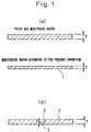
- Fig. 1 (a) is a drawing that shows the structure of an example of a wafer for heavy metal monitoring according to the present invention, with Fig. 1 (a) showing a wafer for heavy metal monitoring, wherein for the purpose of monitoring the amount of heavy metal contamination on a wafer, the thickness t of a wafer 1 is made smaller than a prescribed standard wafer thickness T with respect to the wafer diameter.
- the present invention makes the wafer thickness 675 ⁇ m, so that it is possible to maintain a correct correlation between the sensitivity coefficient and the heavy metal contamination amount.
- Fig. 2 is a flowchart that shows the method for manufacturing a heavy metal monitor wafer according to the present invention, this drawing showing a method for manufacturing a wafer for monitoring heavy metals contamination in a wafer by measuring minority carrier lifetime, the method including a first step of thermal treatment to the wafer at a temperature in the range from 1150 °C to 1350 °C in an atmosphere of O 2 + He or an atmosphere of H 2 + He, and a second step of thermal treatment to the wafer at a temperature in the range from 900 °C to 1000 °C in an atmosphere of N 2 + O 2 or an atmosphere of O 2 .
- the temperature is set in the range from 1150 °C to 1350 °C, and to eliminate errors that occur in the minority carrier lifetime because of crystal defects, a thermal treating step is provided which is performed in an inert light element gas atmosphere of H 2 or He.
- Fig. 1 (b) is a drawing that shows the structure of another embodiment of a wafer for heavy metal monitoring, and Fig. 1 (b) shows a heavy metal monitoring water in which a heavy metal monitoring region 3 is provided on a wafer 2, the thickness t of this heavy metal monitoring region 3 being less than a prescribed standard wafer thickness T with respect to the diameter of the wafer 2.
- a chip for the purpose of monitoring lifetime is provided in a thin part having a thickness of 675 ⁇ m at the region 3 in the center part of the wafer.
- the thickness in the above-noted region 3 in the center part can be set in the range from 250 ⁇ m to 700 ⁇ m, and this region does not absolutely need to be provided in the center part of the wafer.
- the thickness of the wafer used for monitoring is established so as to be 675 ⁇ m, which is less than the standard wafer thickness, this type of wafer being used to perform lifetime measurement, thereby enabling the maintenance of a correctly correlated sensitivity coefficient, obtained from the correlation between the heavy metal contamination amount and the lifetime value, thereby enabling an improvement in measurement accuracy.
Landscapes
- Testing Or Measuring Of Semiconductors Or The Like (AREA)
Applications Claiming Priority (2)
| Application Number | Priority Date | Filing Date | Title |
|---|---|---|---|
| JP19350798A JP3204309B2 (ja) | 1998-07-09 | 1998-07-09 | 重金属汚染のモニタ方法 |
| JP19350798 | 1998-07-09 |
Publications (1)
| Publication Number | Publication Date |
|---|---|
| EP0971402A2 true EP0971402A2 (de) | 2000-01-12 |
Family
ID=16309214
Family Applications (1)
| Application Number | Title | Priority Date | Filing Date |
|---|---|---|---|
| EP99113170A Withdrawn EP0971402A2 (de) | 1998-07-09 | 1999-07-07 | Wafer zur Überwachung von Schwermetallen und dessen Herstellungsmethode |
Country Status (5)
| Country | Link |
|---|---|
| US (1) | US6518785B2 (de) |
| EP (1) | EP0971402A2 (de) |
| JP (1) | JP3204309B2 (de) |
| KR (1) | KR100333517B1 (de) |
| TW (1) | TW448526B (de) |
Families Citing this family (7)
| Publication number | Priority date | Publication date | Assignee | Title |
|---|---|---|---|---|
| WO2009020783A2 (en) * | 2007-08-06 | 2009-02-12 | Oft Labs Llc | Methods for collection of oral fluid |
| US7829340B2 (en) | 2007-08-06 | 2010-11-09 | Oft Labs, Llc | Oral fluid assays for the detection of heavy metal exposure |
| KR101007441B1 (ko) * | 2008-07-14 | 2011-01-12 | 주식회사 엘지실트론 | 웨이퍼의 벌크금속 분석방법 |
| US8534176B2 (en) | 2008-11-19 | 2013-09-17 | Philadelphia Health & Education Corporation | Method and apparatus for braiding micro strands |
| WO2012135227A2 (en) * | 2011-03-29 | 2012-10-04 | Eddie Reed | Methods and systems for assessing exposure to heavy metals |
| CN102759695B (zh) * | 2012-07-10 | 2015-10-28 | 江西赛维Ldk太阳能高科技有限公司 | 一种判断硅块质量的方法及装置 |
| JP7249395B1 (ja) * | 2021-11-10 | 2023-03-30 | 株式会社Sumco | 半導体試料の評価方法、半導体試料の評価装置および半導体ウェーハの製造方法 |
Family Cites Families (8)
| Publication number | Priority date | Publication date | Assignee | Title |
|---|---|---|---|---|
| US4668330A (en) * | 1985-12-05 | 1987-05-26 | Monsanto Company | Furnace contamination |
| US4706493A (en) | 1985-12-13 | 1987-11-17 | General Motors Corporation | Semiconductor gas sensor having thermally isolated site |
| JP2985583B2 (ja) | 1993-05-31 | 1999-12-06 | 信越半導体株式会社 | シリコンウエーハの鏡面加工表面における加工変質層検査方法とその厚さ測定方法 |
| US5418172A (en) * | 1993-06-29 | 1995-05-23 | Memc Electronic Materials S.P.A. | Method for detecting sources of contamination in silicon using a contamination monitor wafer |
| JP3005426B2 (ja) | 1994-07-25 | 2000-01-31 | 大日本スクリーン製造株式会社 | 半導体ウェハ電気的測定装置 |
| US5788763A (en) * | 1995-03-09 | 1998-08-04 | Toshiba Ceramics Co., Ltd. | Manufacturing method of a silicon wafer having a controlled BMD concentration |
| US5698771A (en) | 1995-03-30 | 1997-12-16 | The United States Of America As Represented By The United States National Aeronautics And Space Administration | Varying potential silicon carbide gas sensor |
| JPH1070165A (ja) | 1996-08-27 | 1998-03-10 | Hitachi Ltd | 半導体のライフタイムの計測方法 |
-
1998
- 1998-07-09 JP JP19350798A patent/JP3204309B2/ja not_active Expired - Fee Related
-
1999
- 1999-07-06 KR KR19990027044A patent/KR100333517B1/ko not_active Expired - Fee Related
- 1999-07-07 EP EP99113170A patent/EP0971402A2/de not_active Withdrawn
- 1999-07-07 TW TW088111630A patent/TW448526B/zh active
-
2001
- 2001-11-05 US US10/008,030 patent/US6518785B2/en not_active Expired - Fee Related
Also Published As
| Publication number | Publication date |
|---|---|
| TW448526B (en) | 2001-08-01 |
| US6518785B2 (en) | 2003-02-11 |
| US20020039650A1 (en) | 2002-04-04 |
| KR100333517B1 (ko) | 2002-04-25 |
| KR20000011513A (ko) | 2000-02-25 |
| JP3204309B2 (ja) | 2001-09-04 |
| JP2000031227A (ja) | 2000-01-28 |
Similar Documents
| Publication | Publication Date | Title |
|---|---|---|
| US7888265B2 (en) | Method for assaying copper in silicon wafers | |
| KR100298529B1 (ko) | 실리콘에서의오염물제거와소수캐리어수명개선을위한방법 | |
| US20220146444A1 (en) | Method for measuring resistivity of silicon single crystal | |
| US6200872B1 (en) | Semiconductor substrate processing method | |
| US6344092B1 (en) | Epitaxial semiconductor substrate, manufacturing method thereof, manufacturing method of semiconductor device and manufacturing method of solid-state imaging device | |
| US6632688B2 (en) | Method for evaluating impurity concentrations in epitaxial reagent gases | |
| US6518785B2 (en) | Method for monitoring an amount of heavy metal contamination in a wafer | |
| JP5561245B2 (ja) | 半導体基板の評価方法 | |
| US4420722A (en) | Testing semiconductor furnaces for heavy metal contamination | |
| US4668330A (en) | Furnace contamination | |
| US9935021B2 (en) | Method for evaluating a semiconductor wafer | |
| US5926691A (en) | Methods of fabricating borophosphosilicate glass (BPSG) films having impurity concentrations which remain stable over time, and for using such films testing of microelectronic devices | |
| US20040135208A1 (en) | Semiconductor substrate and manufacturing method thereof | |
| US6358761B1 (en) | Silicon monitor for detection of H2O2 in acid bath | |
| JP3896919B2 (ja) | シリコンウエーハのNi汚染の評価方法 | |
| JP2009266835A (ja) | シリコン単結晶の金属汚染評価方法 | |
| US6013556A (en) | Method of integrated circuit fabrication | |
| EP1933372A1 (de) | Prozess zum herstellen eines epitaxialwafers und dadurch hergestellter epitaxialwafer | |
| US20090087807A1 (en) | Method of semiconductor process and semiconductor apparatus system | |
| KR102719439B1 (ko) | 실리콘 웨이퍼의 산화물층의 두께 예측 방법 | |
| KR20090116646A (ko) | 실리콘 웨이퍼 및 이의 제조방법 | |
| CN121191999A (zh) | 单片式热处理炉的金属污染评价方法以及半导体晶片的制造方法 | |
| KR940000914B1 (ko) | 산화막 드라이 에칭용 페데스탈 | |
| CN121463742A (zh) | 基于化学清洗的背封硅片翘曲调控方法 | |
| KR101820680B1 (ko) | 반도체 기판 제조 방법 |
Legal Events
| Date | Code | Title | Description |
|---|---|---|---|
| PUAI | Public reference made under article 153(3) epc to a published international application that has entered the european phase |
Free format text: ORIGINAL CODE: 0009012 |
|
| AK | Designated contracting states |
Kind code of ref document: A2 Designated state(s): AT BE CH CY DE DK ES FI FR GB GR IE IT LI LU MC NL PT SE |
|
| AX | Request for extension of the european patent |
Free format text: AL;LT;LV;MK;RO;SI |
|
| RAP1 | Party data changed (applicant data changed or rights of an application transferred) |
Owner name: NEC ELECTRONICS CORPORATION |
|
| STAA | Information on the status of an ep patent application or granted ep patent |
Free format text: STATUS: THE APPLICATION HAS BEEN WITHDRAWN |
|
| 18W | Application withdrawn |
Effective date: 20040519 |