EP0971402A2 - Wafer for heavy metal monitoring and method for manufacturing same - Google Patents
Wafer for heavy metal monitoring and method for manufacturing same Download PDFInfo
- Publication number
- EP0971402A2 EP0971402A2 EP99113170A EP99113170A EP0971402A2 EP 0971402 A2 EP0971402 A2 EP 0971402A2 EP 99113170 A EP99113170 A EP 99113170A EP 99113170 A EP99113170 A EP 99113170A EP 0971402 A2 EP0971402 A2 EP 0971402A2
- Authority
- EP
- European Patent Office
- Prior art keywords
- wafer
- heavy metal
- thickness
- monitoring
- atmosphere
- Prior art date
- Legal status (The legal status is an assumption and is not a legal conclusion. Google has not performed a legal analysis and makes no representation as to the accuracy of the status listed.)
- Withdrawn
Links
Images

Classifications
-
- H—ELECTRICITY
- H10—SEMICONDUCTOR DEVICES; ELECTRIC SOLID-STATE DEVICES NOT OTHERWISE PROVIDED FOR
- H10P—GENERIC PROCESSES OR APPARATUS FOR THE MANUFACTURE OR TREATMENT OF DEVICES COVERED BY CLASS H10
- H10P74/00—Testing or measuring during manufacture or treatment of wafers, substrates or devices
- H10P74/27—Structural arrangements therefor
- H10P74/277—Circuits for electrically characterising or monitoring manufacturing processes, e.g. circuits in tested chips or circuits in testing wafers
-
- Y—GENERAL TAGGING OF NEW TECHNOLOGICAL DEVELOPMENTS; GENERAL TAGGING OF CROSS-SECTIONAL TECHNOLOGIES SPANNING OVER SEVERAL SECTIONS OF THE IPC; TECHNICAL SUBJECTS COVERED BY FORMER USPC CROSS-REFERENCE ART COLLECTIONS [XRACs] AND DIGESTS
- Y10—TECHNICAL SUBJECTS COVERED BY FORMER USPC
- Y10T—TECHNICAL SUBJECTS COVERED BY FORMER US CLASSIFICATION
- Y10T428/00—Stock material or miscellaneous articles
- Y10T428/26—Web or sheet containing structurally defined element or component, the element or component having a specified physical dimension
- Y10T428/266—Web or sheet containing structurally defined element or component, the element or component having a specified physical dimension of base or substrate
Definitions
- the present invention relates to a wafer for a heavy metal monitor and a method for manufacturing such a wafer, and more particularly to a method for manufacturing a wafer which is capable of measuring the degree of heavy metal contamination with good accuracy, even in a manufacturing process in which a large-diameter wafer of 8 inches or 12 inches and over is being processed, and to a method for manufacturing such a wafer.
- the wafer that is used for this monitoring be the same size as the wafer being processed, as the size of silicon wafers grew, in order to achieve rigidity with respect to stress, the thickness of the wafer grew large, the result being that the apparent lifetime became long, this hindering measurement with good accuracy.
- Fig. 3 shows the method of manufacturing a wafer used for heavy metal monitoring in the past. This wafer is subjected to thermal oxidation at a temperature in the range from 900 °C to 1000 °C in an atmosphere of O 2 or in an atmosphere of N 2 and O 2 , thereby achieving thermal treating for the purpose of preventing surface recombination.
- a metal such as titanium which has a low diffusion coefficient, is introduced into the oxide film during thermal treating, in which case there is a further deterioration of the measurement accuracy.
- Another object of the present invention is to provide a novel method for manufacturing a wafer for monitoring heavy metal contamination that is capable of measuring of the amount of metal contamination with good accuracy, while suppressing the measurement error that is introduced by the introduction of a metal such as titanium, which has a low diffusion coefficient, into the oxide film.
- the present invention adopts the following basic technical constitution.
- the first aspect of the present invention is a wafer for heavy metal monitoring, said wafer having, for monitoring an amount of heavy metal contamination in a wafer, a thickness thereof that is less than a prescribed standard wafer thickness as defined with respect to the wafer diameter.
- the thickness of the wafer is in the range from 250 ⁇ m to 750 ⁇ m.
- heavy metal monitoring region is provided on the wafer, the thickness of the wafer in this region being less than a prescribed standard wafer thickness as defined with respect to the wafer diameter.
- the heavy metal monitoring region is provided in the approximate center part of the wafer.
- the thickness of the heavy metal monitoring region is in the range from 250 ⁇ m to 750 ⁇ m.
- the first aspect of a method for manufacturing a wafer is a method for manufacturing a wafer for monitoring the heavy metal contamination on a wafer, this method comprising;
- the thickness of the wafer is less than a prescribed standard wafer thickness as defined with respect to the wafer diameter.
- a wafer for heavy metal monitoring In order to monitor the amount of heavy metal contamination on a wafer, a wafer for heavy metal monitoring according to the present invention has a thickness thereof that is less than a prescribed standard wafer thickness as defined with respect to the wafer diameter, and is capable of measuring the amount of heavy metal contamination with good accuracy, with reduced measurement error.
- a method of manufacturing a wafer for monitoring the amount of heavy metal contamination on a wafer, by measuring minority carriers lifetime having a first step of thermal treatment at a temperature in the range from 1150 °C to 1350 °C in an inert light element gas atmosphere of O 2 + He or an atmosphere of H 2 + He, and a second step of thermal treatment at a temperature in the range from 900 °C to 1000 °C in an atmosphere of N 2 + O 2 or an atmosphere of O 2 , and by means of these steps, it is possible to eliminate the measurement error that occurs because of the inclusion of a metal such as titanium, which has a low diffusion coefficient, into the oxide film during thermal treating, thereby resulting in the achievement of good measurement accuracy.
- Fig. 1 (a) is a drawing that shows the structure of an example of a wafer for heavy metal monitoring according to the present invention, with Fig. 1 (a) showing a wafer for heavy metal monitoring, wherein for the purpose of monitoring the amount of heavy metal contamination on a wafer, the thickness t of a wafer 1 is made smaller than a prescribed standard wafer thickness T with respect to the wafer diameter.
- the present invention makes the wafer thickness 675 ⁇ m, so that it is possible to maintain a correct correlation between the sensitivity coefficient and the heavy metal contamination amount.
- Fig. 2 is a flowchart that shows the method for manufacturing a heavy metal monitor wafer according to the present invention, this drawing showing a method for manufacturing a wafer for monitoring heavy metals contamination in a wafer by measuring minority carrier lifetime, the method including a first step of thermal treatment to the wafer at a temperature in the range from 1150 °C to 1350 °C in an atmosphere of O 2 + He or an atmosphere of H 2 + He, and a second step of thermal treatment to the wafer at a temperature in the range from 900 °C to 1000 °C in an atmosphere of N 2 + O 2 or an atmosphere of O 2 .
- the temperature is set in the range from 1150 °C to 1350 °C, and to eliminate errors that occur in the minority carrier lifetime because of crystal defects, a thermal treating step is provided which is performed in an inert light element gas atmosphere of H 2 or He.
- Fig. 1 (b) is a drawing that shows the structure of another embodiment of a wafer for heavy metal monitoring, and Fig. 1 (b) shows a heavy metal monitoring water in which a heavy metal monitoring region 3 is provided on a wafer 2, the thickness t of this heavy metal monitoring region 3 being less than a prescribed standard wafer thickness T with respect to the diameter of the wafer 2.
- a chip for the purpose of monitoring lifetime is provided in a thin part having a thickness of 675 ⁇ m at the region 3 in the center part of the wafer.
- the thickness in the above-noted region 3 in the center part can be set in the range from 250 ⁇ m to 700 ⁇ m, and this region does not absolutely need to be provided in the center part of the wafer.
- the thickness of the wafer used for monitoring is established so as to be 675 ⁇ m, which is less than the standard wafer thickness, this type of wafer being used to perform lifetime measurement, thereby enabling the maintenance of a correctly correlated sensitivity coefficient, obtained from the correlation between the heavy metal contamination amount and the lifetime value, thereby enabling an improvement in measurement accuracy.
Landscapes
- Testing Or Measuring Of Semiconductors Or The Like (AREA)
Abstract
In order to monitor the amount of heavy metal
contamination on a semiconductor wafer, the thickness of a
monitor wafer is made smaller than a prescribed standard
thickness with respect to the wafer diameter.
Description
- The present invention relates to a wafer for a heavy metal monitor and a method for manufacturing such a wafer, and more particularly to a method for manufacturing a wafer which is capable of measuring the degree of heavy metal contamination with good accuracy, even in a manufacturing process in which a large-diameter wafer of 8 inches or 12 inches and over is being processed, and to a method for manufacturing such a wafer.
- In the past, in a process for manufacturing a semiconductor, heavy metal contamination, which causes a deterioration of the characteristics of a semiconductor, such as with regard to leakage, was measured and monitored by a minority carrier lifetime measurement apparatus which made use of the µ-PCD method (microwave photoconductive decay).
- In particular, because it was advantageous to have the wafer that is used for this monitoring be the same size as the wafer being processed, as the size of silicon wafers grew, in order to achieve rigidity with respect to stress, the thickness of the wafer grew large, the result being that the apparent lifetime became long, this hindering measurement with good accuracy.
- Fig. 3 shows the method of manufacturing a wafer used for heavy metal monitoring in the past. This wafer is subjected to thermal oxidation at a temperature in the range from 900 °C to 1000 °C in an atmosphere of O2 or in an atmosphere of N2 and O2, thereby achieving thermal treating for the purpose of preventing surface recombination.
- However, a metal such as titanium, which has a low diffusion coefficient, is introduced into the oxide film during thermal treating, in which case there is a further deterioration of the measurement accuracy.
- Accordingly, it is an object of the present invention to improve on the drawbacks of the prior as noted above, by providing a novel wafer which enables measurement of the amount of heavy metal contamination with good accuracy, even in a process of manufacturing a large-diameter wafer, and a further object to provide a method for manufacturing such a monitoring wafer.
- Another object of the present invention is to provide a novel method for manufacturing a wafer for monitoring heavy metal contamination that is capable of measuring of the amount of metal contamination with good accuracy, while suppressing the measurement error that is introduced by the introduction of a metal such as titanium, which has a low diffusion coefficient, into the oxide film.
- In order to achieve the above-noted objects, the present invention adopts the following basic technical constitution.
- Specifically, the first aspect of the present invention is a wafer for heavy metal monitoring, said wafer having, for monitoring an amount of heavy metal contamination in a wafer, a thickness thereof that is less than a prescribed standard wafer thickness as defined with respect to the wafer diameter.
- In the second aspect of the present invention, the thickness of the wafer is in the range from 250 µm to 750 µm.
- In the third aspect of the present invention, in order to monitor heavy metal contamination in a wafer, heavy metal monitoring region is provided on the wafer, the thickness of the wafer in this region being less than a prescribed standard wafer thickness as defined with respect to the wafer diameter.
- In the fourth aspect of the present invention, the heavy metal monitoring region is provided in the approximate center part of the wafer.
- In the fifth aspect of the present invention, the thickness of the heavy metal monitoring region is in the range from 250 µm to 750 µm.
- The first aspect of a method for manufacturing a wafer is a method for manufacturing a wafer for monitoring the heavy metal contamination on a wafer, this method comprising;
- a first step of thermal treatment to the wafer at a temperature in the range from 1150 °C to 1350 °C in an atmosphere of O2 + He or an atmosphere of H2 + He, and
- a second step of thermal treatment to the wafer at a temperature in the range from 900 °C to 1000 °C in an atmosphere of N2 + O2 or an atmosphere of O2.
-
- In the second aspect of a method for manufacturing a wafer for heavy metal contamination monitoring, the thickness of the wafer is less than a prescribed standard wafer thickness as defined with respect to the wafer diameter.
- In order to monitor the amount of heavy metal contamination on a wafer, a wafer for heavy metal monitoring according to the present invention has a thickness thereof that is less than a prescribed standard wafer thickness as defined with respect to the wafer diameter, and is capable of measuring the amount of heavy metal contamination with good accuracy, with reduced measurement error.
- A method of manufacturing a wafer for monitoring the amount of heavy metal contamination on a wafer, by measuring minority carriers lifetime, this method having a first step of thermal treatment at a temperature in the range from 1150 °C to 1350 °C in an inert light element gas atmosphere of O2 + He or an atmosphere of H2 + He, and a second step of thermal treatment at a temperature in the range from 900 °C to 1000 °C in an atmosphere of N2 + O2 or an atmosphere of O2, and by means of these steps, it is possible to eliminate the measurement error that occurs because of the inclusion of a metal such as titanium, which has a low diffusion coefficient, into the oxide film during thermal treating, thereby resulting in the achievement of good measurement accuracy.
-
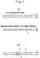
- Fig. 1 is a drawing that shows a monitor wafer according to the present invention, with Fig. 1 (a) being a cross-section view of the wafer, showing the first embodiment, and Fig. 1 (b) being a plan view of a wafer, showing the second embodiment.
- Fig. 2 is a drawing that shows the manufacturing processes for the main part of a monitor wafer according to the present invention.
- Fig. 3 is a drawing that shows the manufacturing processes for a monitor wafer of the prior art.
-
- Embodiments of a wafer for heavy metal monitoring according to the present invention are described in detail below, with references being made to relevant accompanying drawings.
- Fig. 1 (a) is a drawing that shows the structure of an example of a wafer for heavy metal monitoring according to the present invention, with Fig. 1 (a) showing a wafer for heavy metal monitoring, wherein for the purpose of monitoring the amount of heavy metal contamination on a wafer, the thickness t of a wafer 1 is made smaller than a prescribed standard wafer thickness T with respect to the wafer diameter.
- In the manufacturing processes for manufacturing a semiconductor integrated circuit, in the case in which the microwave photoconductive decay method is employed to monitor, by measuring the minority carrier lifetime, the amount of heavy metals, which cause deterioration of the transistor characteristics such as with regard to leakage, whereas in the method of the prior art a heavy metal monitor wafer having a standard thickness (725 µm for an 8-inch wafer, 775 µm for a 12-inch wafer), in the case of the present invention a wafer having a thickness in the range from 250 µm to 700 µm is used.
- In the above-noted case, at below 250 µm, problems arise in the transport of the wafer, for example, due to sag of the wafer because of its thinness. Specifically, it had been advantageous to use a wafer having the same thickness as a 6-inch wafer.
- It has been theoretically and experimentally determined that the minority carrier lifetime that is obtained using the microwave PCD method is lengthened in proportion to the square of the wafer thickness, so that for a given heavy metal contamination level, the apparent lifetime is lengthened. Because of this, the present invention makes the wafer thickness 675 µm, so that it is possible to maintain a correct correlation between the sensitivity coefficient and the heavy metal contamination amount.
- Fig. 2 is a flowchart that shows the method for manufacturing a heavy metal monitor wafer according to the present invention, this drawing showing a method for manufacturing a wafer for monitoring heavy metals contamination in a wafer by measuring minority carrier lifetime, the method including a first step of thermal treatment to the wafer at a temperature in the range from 1150 °C to 1350 °C in an atmosphere of O2 + He or an atmosphere of H2 + He, and a second step of thermal treatment to the wafer at a temperature in the range from 900 °C to 1000 °C in an atmosphere of N2 + O2 or an atmosphere of O2.
- Specifically, in the present invention, in order to prevent as much as possible the intrusion of the heavy metal such as titanium, which has a low diffusion coefficient with respect to silicon, into an oxide film, before the above-noted thermal treating, the temperature is set in the range from 1150 °C to 1350 °C, and to eliminate errors that occur in the minority carrier lifetime because of crystal defects, a thermal treating step is provided which is performed in an inert light element gas atmosphere of H2 or He.
- By virtue of the above-noted constitution, it is possible to suppress the deterioration of the sensitivity coefficient that is caused by inclusion of a metal such as titanium into the oxide film that is formed during thermal oxidation that is performed for the purpose of preventing surface recombination, and it is also possible to eliminate the cause of errors in lifetime decay due to crystal defects.
- Fig. 1 (b) is a drawing that shows the structure of another embodiment of a wafer for heavy metal monitoring, and Fig. 1 (b) shows a heavy metal monitoring water in which a heavy
metal monitoring region 3 is provided on awafer 2, the thickness t of this heavymetal monitoring region 3 being less than a prescribed standard wafer thickness T with respect to the diameter of thewafer 2. - In the past, when the monitor carrier lifetime measurement method was used to monitor heavy metal contamination during the manufacturing process, bare silicon having the standard thickness was used for measurement of the lifetime. In the present invention, however, in order to achieve a high sensitivity in the measurement of lifetime commensurate with advances in the manufacturing processes, a chip for the purpose of monitoring lifetime is provided in a thin part having a thickness of 675 µm at the
region 3 in the center part of the wafer. - Of course, the thickness in the above-noted
region 3 in the center part can be set in the range from 250 µm to 700 µm, and this region does not absolutely need to be provided in the center part of the wafer. - In the present invention, the thickness of the wafer used for monitoring is established so as to be 675 µm, which is less than the standard wafer thickness, this type of wafer being used to perform lifetime measurement, thereby enabling the maintenance of a correctly correlated sensitivity coefficient, obtained from the correlation between the heavy metal contamination amount and the lifetime value, thereby enabling an improvement in measurement accuracy.
Claims (7)
- A wafer for heavy metal monitoring, said wafer having, for monitoring an amount of heavy metal contamination in a wafer, a thickness thereof that is less than a prescribed standard wafer thickness as defined with respect to the wafer diameter.
- A wafer for heavy metal monitoring according to claim 1, wherein the said wafer thickness is in the range from 250 µm to 700 µm.
- A wafer for heavy metal monitoring, said wafer having, for monitoring an amount of heavy metal contamination in a wafer, a region thereon for heavy metal monitoring, the wafer thickness of said region being less than a prescribed standard wafer thickness as defined with respect to the wafer diameter.
- A wafer for heavy metal monitoring according to claim 3, wherein said region for heavy metal monitoring is disposed in the approximate center of said wafer.
- A wafer for heavy metal monitoring according to claim 3, wherein the thickness of said region for heavy metal monitoring is in the range from 250 µm to 700 µm.
- A method for manufacturing a wafer for monitoring heavy metal contamination amount by measuring minority carrier lifetime, said method comprising:a first step of thermal treatment to said wafer at a temperature in the range from 1150 °C to 1350 °C in an atmosphere of O2 + He or an atmosphere of H2 + He, anda second step of thermal treatment to said wafer at a temperature in the range from 900 °C to 1000 °C in an atmosphere of N2 + O2 or an atmosphere of O2.
- A method for manufacturing a wafer for heavy metal monitoring according to claim 6, wherein the thickness of said wafer is less than a prescribed standard wafer thickness as defined with respect to the wafer diameter.
Applications Claiming Priority (2)
| Application Number | Priority Date | Filing Date | Title |
|---|---|---|---|
| JP19350798 | 1998-07-09 | ||
| JP19350798A JP3204309B2 (en) | 1998-07-09 | 1998-07-09 | How to monitor heavy metal contamination |
Publications (1)
| Publication Number | Publication Date |
|---|---|
| EP0971402A2 true EP0971402A2 (en) | 2000-01-12 |
Family
ID=16309214
Family Applications (1)
| Application Number | Title | Priority Date | Filing Date |
|---|---|---|---|
| EP99113170A Withdrawn EP0971402A2 (en) | 1998-07-09 | 1999-07-07 | Wafer for heavy metal monitoring and method for manufacturing same |
Country Status (5)
| Country | Link |
|---|---|
| US (1) | US6518785B2 (en) |
| EP (1) | EP0971402A2 (en) |
| JP (1) | JP3204309B2 (en) |
| KR (1) | KR100333517B1 (en) |
| TW (1) | TW448526B (en) |
Families Citing this family (7)
| Publication number | Priority date | Publication date | Assignee | Title |
|---|---|---|---|---|
| WO2009020782A2 (en) * | 2007-08-06 | 2009-02-12 | Oft Labs Llc | Oral fluid assays for the detection of heavy metal exposure |
| US20090043226A1 (en) * | 2007-08-06 | 2009-02-12 | Oft Labs, Llc | Methods for Collection of Oral Fluid |
| KR101007441B1 (en) * | 2008-07-14 | 2011-01-12 | 주식회사 엘지실트론 | Bulk Metal Wafer Analysis Method |
| WO2010059832A1 (en) | 2008-11-19 | 2010-05-27 | Drexel University | Method and apparatus for braiding micro strands |
| WO2012135227A2 (en) * | 2011-03-29 | 2012-10-04 | Eddie Reed | Methods and systems for assessing exposure to heavy metals |
| CN102759695B (en) * | 2012-07-10 | 2015-10-28 | 江西赛维Ldk太阳能高科技有限公司 | A kind of method and device judging silico briquette quality |
| JP7249395B1 (en) * | 2021-11-10 | 2023-03-30 | 株式会社Sumco | Semiconductor sample evaluation method, semiconductor sample evaluation device, and semiconductor wafer manufacturing method |
Family Cites Families (8)
| Publication number | Priority date | Publication date | Assignee | Title |
|---|---|---|---|---|
| US4668330A (en) * | 1985-12-05 | 1987-05-26 | Monsanto Company | Furnace contamination |
| US4706493A (en) | 1985-12-13 | 1987-11-17 | General Motors Corporation | Semiconductor gas sensor having thermally isolated site |
| JP2985583B2 (en) | 1993-05-31 | 1999-12-06 | 信越半導体株式会社 | Inspection method of damaged layer on mirror-finished surface of silicon wafer and thickness measurement method |
| US5418172A (en) * | 1993-06-29 | 1995-05-23 | Memc Electronic Materials S.P.A. | Method for detecting sources of contamination in silicon using a contamination monitor wafer |
| JP3005426B2 (en) | 1994-07-25 | 2000-01-31 | 大日本スクリーン製造株式会社 | Semiconductor wafer electrical measurement device |
| US5788763A (en) * | 1995-03-09 | 1998-08-04 | Toshiba Ceramics Co., Ltd. | Manufacturing method of a silicon wafer having a controlled BMD concentration |
| US5698771A (en) | 1995-03-30 | 1997-12-16 | The United States Of America As Represented By The United States National Aeronautics And Space Administration | Varying potential silicon carbide gas sensor |
| JPH1070165A (en) | 1996-08-27 | 1998-03-10 | Hitachi Ltd | Semiconductor Lifetime Measurement Method |
-
1998
- 1998-07-09 JP JP19350798A patent/JP3204309B2/en not_active Expired - Fee Related
-
1999
- 1999-07-06 KR KR19990027044A patent/KR100333517B1/en not_active Expired - Fee Related
- 1999-07-07 TW TW088111630A patent/TW448526B/en active
- 1999-07-07 EP EP99113170A patent/EP0971402A2/en not_active Withdrawn
-
2001
- 2001-11-05 US US10/008,030 patent/US6518785B2/en not_active Expired - Fee Related
Also Published As
| Publication number | Publication date |
|---|---|
| KR100333517B1 (en) | 2002-04-25 |
| JP3204309B2 (en) | 2001-09-04 |
| TW448526B (en) | 2001-08-01 |
| KR20000011513A (en) | 2000-02-25 |
| US20020039650A1 (en) | 2002-04-04 |
| JP2000031227A (en) | 2000-01-28 |
| US6518785B2 (en) | 2003-02-11 |
Similar Documents
| Publication | Publication Date | Title |
|---|---|---|
| US7888265B2 (en) | Method for assaying copper in silicon wafers | |
| KR100298529B1 (en) | Methods for removing contaminants from silicon and improving minority carrier life | |
| US20220146444A1 (en) | Method for measuring resistivity of silicon single crystal | |
| US6200872B1 (en) | Semiconductor substrate processing method | |
| US6344092B1 (en) | Epitaxial semiconductor substrate, manufacturing method thereof, manufacturing method of semiconductor device and manufacturing method of solid-state imaging device | |
| US6632688B2 (en) | Method for evaluating impurity concentrations in epitaxial reagent gases | |
| US6518785B2 (en) | Method for monitoring an amount of heavy metal contamination in a wafer | |
| JP5561245B2 (en) | Semiconductor substrate evaluation method | |
| US4420722A (en) | Testing semiconductor furnaces for heavy metal contamination | |
| US4668330A (en) | Furnace contamination | |
| US5926691A (en) | Methods of fabricating borophosphosilicate glass (BPSG) films having impurity concentrations which remain stable over time, and for using such films testing of microelectronic devices | |
| US9935021B2 (en) | Method for evaluating a semiconductor wafer | |
| US20040135208A1 (en) | Semiconductor substrate and manufacturing method thereof | |
| US6358761B1 (en) | Silicon monitor for detection of H2O2 in acid bath | |
| JP3896919B2 (en) | Method for evaluating Ni contamination of silicon wafer | |
| JP2009266835A (en) | Metal contamination evaluating method of silicon single crystal | |
| US6013556A (en) | Method of integrated circuit fabrication | |
| US7806684B2 (en) | Method of semiconductor process and semiconductor apparatus system | |
| EP1933372A1 (en) | Process for producing epitaxial wafer and epitaxial wafer produced therefrom | |
| KR102719439B1 (en) | Method for predicting thickness of oxide layer of silicon wafer | |
| KR20090116646A (en) | Silicon wafer and its manufacturing method | |
| CN121191999A (en) | Methods for evaluating metal contamination in single-piece heat treatment furnaces and methods for manufacturing semiconductor wafers. | |
| KR940000914B1 (en) | Pedestal for dry etching process of oxide film | |
| CN121463742A (en) | Chemical Cleaning-Based Warpage Control Method for Back-Sealed Silicon Wafers | |
| KR101820680B1 (en) | Method for manufacturing semiconductor substrate |
Legal Events
| Date | Code | Title | Description |
|---|---|---|---|
| PUAI | Public reference made under article 153(3) epc to a published international application that has entered the european phase |
Free format text: ORIGINAL CODE: 0009012 |
|
| AK | Designated contracting states |
Kind code of ref document: A2 Designated state(s): AT BE CH CY DE DK ES FI FR GB GR IE IT LI LU MC NL PT SE |
|
| AX | Request for extension of the european patent |
Free format text: AL;LT;LV;MK;RO;SI |
|
| RAP1 | Party data changed (applicant data changed or rights of an application transferred) |
Owner name: NEC ELECTRONICS CORPORATION |
|
| STAA | Information on the status of an ep patent application or granted ep patent |
Free format text: STATUS: THE APPLICATION HAS BEEN WITHDRAWN |
|
| 18W | Application withdrawn |
Effective date: 20040519 |