EP0970086B1 - Spiroverbindungen und deren verwendung - Google Patents
Spiroverbindungen und deren verwendung Download PDFInfo
- Publication number
- EP0970086B1 EP0970086B1 EP98913731A EP98913731A EP0970086B1 EP 0970086 B1 EP0970086 B1 EP 0970086B1 EP 98913731 A EP98913731 A EP 98913731A EP 98913731 A EP98913731 A EP 98913731A EP 0970086 B1 EP0970086 B1 EP 0970086B1
- Authority
- EP
- European Patent Office
- Prior art keywords
- replaced
- groups
- naphthyl
- different
- und
- Prior art date
- Legal status (The legal status is an assumption and is not a legal conclusion. Google has not performed a legal analysis and makes no representation as to the accuracy of the status listed.)
- Expired - Lifetime
Links
- 0 CC(*1)=C(*)C2=C1C(*C(N)=C)=C(*)[C@]21C(C(*)=C(*2)N)=C2C2=C1C(*)=C(**)*2 Chemical compound CC(*1)=C(*)C2=C1C(*C(N)=C)=C(*)[C@]21C(C(*)=C(*2)N)=C2C2=C1C(*)=C(**)*2 0.000 description 11
- QXBUYALKJGBACG-UHFFFAOYSA-N CN1c2ccccc2Sc2c1cccc2 Chemical compound CN1c2ccccc2Sc2c1cccc2 QXBUYALKJGBACG-UHFFFAOYSA-N 0.000 description 1
Images

Classifications
-
- C—CHEMISTRY; METALLURGY
- C07—ORGANIC CHEMISTRY
- C07D—HETEROCYCLIC COMPOUNDS
- C07D471/00—Heterocyclic compounds containing nitrogen atoms as the only ring hetero atoms in the condensed system, at least one ring being a six-membered ring with one nitrogen atom, not provided for by groups C07D451/00 - C07D463/00
- C07D471/02—Heterocyclic compounds containing nitrogen atoms as the only ring hetero atoms in the condensed system, at least one ring being a six-membered ring with one nitrogen atom, not provided for by groups C07D451/00 - C07D463/00 in which the condensed system contains two hetero rings
- C07D471/10—Spiro-condensed systems
-
- C—CHEMISTRY; METALLURGY
- C09—DYES; PAINTS; POLISHES; NATURAL RESINS; ADHESIVES; COMPOSITIONS NOT OTHERWISE PROVIDED FOR; APPLICATIONS OF MATERIALS NOT OTHERWISE PROVIDED FOR
- C09K—MATERIALS FOR MISCELLANEOUS APPLICATIONS, NOT PROVIDED FOR ELSEWHERE
- C09K11/00—Luminescent materials, e.g. electroluminescent or chemiluminescent
- C09K11/06—Luminescent materials, e.g. electroluminescent or chemiluminescent containing organic luminescent materials
-
- H—ELECTRICITY
- H10—SEMICONDUCTOR DEVICES; ELECTRIC SOLID-STATE DEVICES NOT OTHERWISE PROVIDED FOR
- H10K—ORGANIC ELECTRIC SOLID-STATE DEVICES
- H10K85/00—Organic materials used in the body or electrodes of devices covered by this subclass
- H10K85/60—Organic compounds having low molecular weight
- H10K85/615—Polycyclic condensed aromatic hydrocarbons, e.g. anthracene
- H10K85/626—Polycyclic condensed aromatic hydrocarbons, e.g. anthracene containing more than one polycyclic condensed aromatic rings, e.g. bis-anthracene
-
- H—ELECTRICITY
- H10—SEMICONDUCTOR DEVICES; ELECTRIC SOLID-STATE DEVICES NOT OTHERWISE PROVIDED FOR
- H10K—ORGANIC ELECTRIC SOLID-STATE DEVICES
- H10K85/00—Organic materials used in the body or electrodes of devices covered by this subclass
- H10K85/60—Organic compounds having low molecular weight
- H10K85/649—Aromatic compounds comprising a hetero atom
- H10K85/657—Polycyclic condensed heteroaromatic hydrocarbons
-
- H—ELECTRICITY
- H10—SEMICONDUCTOR DEVICES; ELECTRIC SOLID-STATE DEVICES NOT OTHERWISE PROVIDED FOR
- H10K—ORGANIC ELECTRIC SOLID-STATE DEVICES
- H10K85/00—Organic materials used in the body or electrodes of devices covered by this subclass
- H10K85/60—Organic compounds having low molecular weight
- H10K85/649—Aromatic compounds comprising a hetero atom
- H10K85/657—Polycyclic condensed heteroaromatic hydrocarbons
- H10K85/6572—Polycyclic condensed heteroaromatic hydrocarbons comprising only nitrogen in the heteroaromatic polycondensed ring system, e.g. phenanthroline or carbazole
-
- H—ELECTRICITY
- H10—SEMICONDUCTOR DEVICES; ELECTRIC SOLID-STATE DEVICES NOT OTHERWISE PROVIDED FOR
- H10K—ORGANIC ELECTRIC SOLID-STATE DEVICES
- H10K30/00—Organic devices sensitive to infrared radiation, light, electromagnetic radiation of shorter wavelength or corpuscular radiation
- H10K30/10—Organic devices sensitive to infrared radiation, light, electromagnetic radiation of shorter wavelength or corpuscular radiation comprising heterojunctions between organic semiconductors and inorganic semiconductors
- H10K30/15—Sensitised wide-bandgap semiconductor devices, e.g. dye-sensitised TiO2
- H10K30/151—Sensitised wide-bandgap semiconductor devices, e.g. dye-sensitised TiO2 the wide bandgap semiconductor comprising titanium oxide, e.g. TiO2
-
- H—ELECTRICITY
- H10—SEMICONDUCTOR DEVICES; ELECTRIC SOLID-STATE DEVICES NOT OTHERWISE PROVIDED FOR
- H10K—ORGANIC ELECTRIC SOLID-STATE DEVICES
- H10K30/00—Organic devices sensitive to infrared radiation, light, electromagnetic radiation of shorter wavelength or corpuscular radiation
- H10K30/50—Photovoltaic [PV] devices
-
- H—ELECTRICITY
- H10—SEMICONDUCTOR DEVICES; ELECTRIC SOLID-STATE DEVICES NOT OTHERWISE PROVIDED FOR
- H10K—ORGANIC ELECTRIC SOLID-STATE DEVICES
- H10K85/00—Organic materials used in the body or electrodes of devices covered by this subclass
- H10K85/30—Coordination compounds
- H10K85/341—Transition metal complexes, e.g. Ru(II)polypyridine complexes
- H10K85/344—Transition metal complexes, e.g. Ru(II)polypyridine complexes comprising ruthenium
-
- H—ELECTRICITY
- H10—SEMICONDUCTOR DEVICES; ELECTRIC SOLID-STATE DEVICES NOT OTHERWISE PROVIDED FOR
- H10K—ORGANIC ELECTRIC SOLID-STATE DEVICES
- H10K85/00—Organic materials used in the body or electrodes of devices covered by this subclass
- H10K85/60—Organic compounds having low molecular weight
- H10K85/631—Amine compounds having at least two aryl rest on at least one amine-nitrogen atom, e.g. triphenylamine
-
- H—ELECTRICITY
- H10—SEMICONDUCTOR DEVICES; ELECTRIC SOLID-STATE DEVICES NOT OTHERWISE PROVIDED FOR
- H10K—ORGANIC ELECTRIC SOLID-STATE DEVICES
- H10K85/00—Organic materials used in the body or electrodes of devices covered by this subclass
- H10K85/60—Organic compounds having low molecular weight
- H10K85/649—Aromatic compounds comprising a hetero atom
-
- H—ELECTRICITY
- H10—SEMICONDUCTOR DEVICES; ELECTRIC SOLID-STATE DEVICES NOT OTHERWISE PROVIDED FOR
- H10K—ORGANIC ELECTRIC SOLID-STATE DEVICES
- H10K85/00—Organic materials used in the body or electrodes of devices covered by this subclass
- H10K85/60—Organic compounds having low molecular weight
- H10K85/649—Aromatic compounds comprising a hetero atom
- H10K85/652—Cyanine dyes
-
- H—ELECTRICITY
- H10—SEMICONDUCTOR DEVICES; ELECTRIC SOLID-STATE DEVICES NOT OTHERWISE PROVIDED FOR
- H10K—ORGANIC ELECTRIC SOLID-STATE DEVICES
- H10K85/00—Organic materials used in the body or electrodes of devices covered by this subclass
- H10K85/60—Organic compounds having low molecular weight
- H10K85/649—Aromatic compounds comprising a hetero atom
- H10K85/656—Aromatic compounds comprising a hetero atom comprising two or more different heteroatoms per ring
- H10K85/6565—Oxadiazole compounds
-
- Y—GENERAL TAGGING OF NEW TECHNOLOGICAL DEVELOPMENTS; GENERAL TAGGING OF CROSS-SECTIONAL TECHNOLOGIES SPANNING OVER SEVERAL SECTIONS OF THE IPC; TECHNICAL SUBJECTS COVERED BY FORMER USPC CROSS-REFERENCE ART COLLECTIONS [XRACs] AND DIGESTS
- Y02—TECHNOLOGIES OR APPLICATIONS FOR MITIGATION OR ADAPTATION AGAINST CLIMATE CHANGE
- Y02E—REDUCTION OF GREENHOUSE GAS [GHG] EMISSIONS, RELATED TO ENERGY GENERATION, TRANSMISSION OR DISTRIBUTION
- Y02E10/00—Energy generation through renewable energy sources
- Y02E10/50—Photovoltaic [PV] energy
- Y02E10/549—Organic PV cells
Definitions
- EP-A 0 333 641 describes a photoelectrochemical cell which is characterized in that it contains a nanoporous metal oxide semiconductor, ie an extremely roughened and thus enlarged surface. The charge is transported between the semiconductor / chromophore layer and the counter electrode in this cell by means of an electrolyte solution. Although good results are achieved with such cells, the property profile of such a device can still be clearly improved.
- EP-A 0 676 461 uses spiro compounds of the following general formula whereby K 1 and K 2 are independently conjugated systems, in electroluminescent devices.
- the compounds of the formula (I) are preferably amorphous and stand out characterized by high glass transition temperatures.
- the preparation of compounds of the formula (Ia) can, for example, start from from a tetrahalogenation of the spiro base and then Substitution reaction take place (analogous to e.g. US 5,026,894) or via a Tetraacetylation with subsequent C-C linkage after conversion of the Acetyl groups in aldehyde groups or heterocyclic structure after conversion of the Acetyl groups take place in carboxylic acid groups.
- the preparation of compounds of the formula (Ib) can, for example, analogously to those of the formula (la) take place, the stoichiometric ratios in the Implementation can be chosen so that the positions 2.2 'and 7.7' des Spirofluorens corresponding positions can be functionalized (see e.g. J. H. Weisburger, E. K. Weisburger, F. E. Ray, J. Am. Chem. Soc. 1959, 72,4253; F. K. Sutcliffe, H.M. Shahidi, D. Paterson, J. Soc. Dyers Color 1978, 94, 306 and G. Haas, V. Prelog, Helv. Chim. Acta 1969, 52 1202).
- the preparation of compounds of the formula (Ic) can, for example, via a Dibromination in position and subsequent diacetylation in with subsequent Implementation take place analogously to the compounds (la).
- disubstituted pyridines disubstituted pyrazines, disubstituted Pyrimidines and disubstituted pyridazines
- manufacture of disubstituted pyridines, disubstituted pyrazines, disubstituted Pyrimidines and disubstituted pyridazines can be found, for example, in the corresponding volumes of the series "The Chemistry of Heterocyclic Compounds" by A. Weissberger and E. C. Taylor (Editors).
- the spiro compounds of the formula (I) according to the invention are suitable as Charge transport materials, preferably for photovoltaic cells.
- the invention therefore also relates to the use of spiro compounds of formula (I) as a charge transport material, especially for photovoltaic Cells.
- the invention also relates to a photovoltaic cell with a Charge transport layer which has one or more, preferably one, Spiro compounds of the formula (I) contains, preferably consists of them.
- FIG. 1 a preferred embodiment of such a cell 1 is shown (not true to scale).
- a semiconductor 12 which preferably has a surface with a roughness factor> 1
- a conductive carrier 11 which can serve as an electrode or contact and consists, for example, of a metal or indium tin oxide (ITO).
- the cell according to the invention preferably contains a chromophore, shown here as chromophore layer 13, on the surface of the semiconductor.
- the term light-absorbing layer includes both a semiconductor layer and a combination of semiconductor / chromophore, even if the actual absorption in this case takes place almost exclusively through the chromophore.
- the charge transport layer 14 which, according to the invention, contains a spiro compound of the formula (I). It is limited on one side by the counter electrode 15, which can consist, for example, of conductive glass, conductive coated plastic, of metal or of another conductive, preferably light-permeable material.
- the cell 1 is preferably closed off at the top and bottom by an insulating layer 16 and 17, respectively. It can contain a side closure, not shown in the figure, for example a frame made of an electrically insulating material such as plastic or glass. By using a hole conductor material instead of the liquid electrolyte, however, such a side frame is not fundamentally necessary. At least one side of the cell must be permeable for the light to be converted into electrical energy so that it can reach the chromophore or the semiconductor.
- the cell also contains devices, not shown in the figure, for taking off the electrical current generated by the cell.
- the photovoltaic cell according to the invention preferably contains a semiconductor as the light-absorbing layer, which preferably has a very large band gap, particularly preferably at least 3.0 eV, very particularly preferably above 3.0 eV.
- Metal oxide semiconductors in particular the oxides of transition metals, as well as the elements of the third main group and the fourth, fifth and sixth subgroup (of the periodic system of elements) of titanium, zirconium, hafnium, strontium, zinc, indium, yttrium, Lanthanum, vanadium, niobium, tantalum, chromium, molybdenum, tungsten, but also oxides of zinc, iron, nickel or silver, perovskites such as SrTiO 3 , CaTiO 3 , or oxides of other metals of the second and third main group or mixed oxides or oxide mixtures of these metals .
- any other metal oxide with semiconductor properties and a large energy gap (band gap) between the valence band and the conduction band can also
- the semiconductor preferably has a roughness factor greater than 1, particularly preferably greater than 20, very particularly greater than 150.
- the roughness factor is defined as the ratio of a real / effective surface to the area of the projection of this surface of a body, in this case the surface of the semiconductor.
- the roughness factor can be determined, for example, by gravimetric adsorption methods, such as in F. Kohlrausch, Practical Physics, Volume 1, P. 397 (Stuttgart: BG Teubner, 1985).
- the size of the pores is 5-200 nm, preferably 10-50 nm.
- a method for producing polycrystalline metal oxide semiconductor layers using the sol-gel method (described in detail for example in Stalder and Augustynski, J. Electrochem. Soc. 1979, 126, 2007), where the process step of hydrolysis of the metal Alcoholate the percentage relative humidity of the ambient atmosphere can be in a range from 30% to 80% and is kept constant within ⁇ 5%, preferably ⁇ 1%, results in metal oxide semiconductor layers with which a particularly high electrical yield in photovoltaic cells according to the invention can be achieved.
- the rough surface with a polycrystalline structure offers an area larger by the roughness factor for a, preferably, monomolecular surface layer of a chromophore. This ensures that the light incident on an area of a certain size is converted into electrical energy with a significantly higher yield.
- the semiconductor can be viewed as transparent to the incident luminous flux. However, light is partially reflected on the surface and reaches z. T. on neighboring surfaces. The penetrating into the semiconductor and not absorbed or converted light hits z. Sometimes directly and to another part indirectly and to another part indirectly after total reflection on the surface, on the exit side on chromophore molecules, which makes it possible to achieve a significantly higher light output.
- the sensitivity, ie the photoelectronic yield for visible light, including sunlight, can therefore be increased by chemically attaching or storing (chemisorbed) so-called chromophores, also called sensitizers or dyes, as charge carriers on the surface of the semiconductor.
- chromophores also called sensitizers or dyes
- the two functions of light absorption and charge carrier separation are separated in these photoelectronic systems.
- Light absorption is taken over by the chromophore in the surface area, and the charge carriers are separated at the semiconductor / chromophore boundary layer.
- Different chromophores have different spectral sensitivities. The choice of the chromophore can thus be adapted to the spectral composition of the light from the light source in order to increase the yield as much as possible.
- the complexes of transition metals of the metal (L 3 ), metal (L 2 ) type of ruthenium and osmium are particularly suitable as chromophores, ie sensitizers '-dicarboxylic acid) and their salts, ruthenium cis diaqua bipyridyl complexes, such as ruthenium cis-diaqua bis (2,2'bipyridyl-4,4'-dicarboxylate) and porphyrins (e.g. zinc tetra (4-carboxyphenyl) porphyrin) and Cyanides (e.g.
- the chromophores can be chemisorbed, adsorbed or otherwise firmly attached in the area of the surface of the metal oxide semiconductor.
- Favorable results have been achieved, for example, with chromophores which are bonded to the surface of the metal oxide semiconductor with carboxylic acid or phosphonic acid ligands.
- Suitable chromophores are, for example, in Chem. Rev. 1995, 49-68 described.
- ruthenium tris (2,2'-bipyridyl-4,4'-dicarboxylic acid), their salts and the chromophores (VIII) and (IX), their synthesis and properties in J. Chem. Soc. Chem. Comm. 1995, 65 are described.
- the application of the chromophore for example ruthenium tris (2,2'-bipyridyl-4,4'-dicarboxylic acid) or a salt thereof, is carried out e.g. B. by dipping the substrate with the oxide layer in a solution, for example an aqueous or alcoholic, preferably ethanolic, for about an hour.
- a solution for example an aqueous or alcoholic, preferably ethanolic, for about an hour.
- the concentration of Solution is preferably 0.1 to 10 molar, particularly preferably 1 to 5 molar, for example 2 molar.
- Other chromophores can be found using analogous procedures Apply to titanium oxide or other metal oxide semiconductors.
- Suitable electrodes 15 are stable, metallically conductive substances, e.g. B. Au, Ag, Pt, Cu, or other metals. But it can also be used for some applications preferably translucent conductive substances such as doped metal oxides, e.g. B. Indium tin oxide, Sb-doped tin oxide or Al-doped zinc oxide is used will.
- the work function of the electrode material used preferably to the ionization potential of the hole transport material used be adjusted.
- the electrode can, as described in EP-A 0 333 641, on a transparent Substrate, e.g. B. glass, are applied and with the hole transport layer be connected. It can preferably pass through in the cell according to the invention physical deposition methods, e.g. B. vapor deposition or atomization (sputtering), be applied directly to the hole transport layer without a second Glass plate is necessary. This method is preferable in applications where which the weight of the cell is to be reduced.
- a transparent Substrate e.g. B. glass
- sputtering atomization
- the cell can e.g. B. sealed with an adhesive or a film will.
- a photovoltaic cell according to the invention generally has a thickness of 5 to 20 mm (with substrate). To avoid reflection losses, it can be provided with a single, double or multi-layer anti-reflective layer.
- Spiro compounds of the formula (I) are also suitable as Electroluminescent materials.
- electroluminescent materials in the context of the invention are materials that as active layer can be used in an electroluminescent device.
- Active layer means that the layer is capable of when an electrical is applied Field to emit light (light-emitting layer) and / or that they do the injection and / or improves the transport of the positive and / or negative charges (Charge injection or charge transport layer).
- the invention therefore also relates to the use of a spiro compound of formula (I) as an electroluminescent material, i.e. as an active layer in one Electroluminescent device.
- the Spiro compounds of the formula (I) are generally known to those skilled in the art common methods, such as dipping or spin coating, in the form of a Film applied to a substrate.
- the invention is also an electroluminescent device with a or more active layers, at least one of these active layers contains one or more spiro compounds of the formula (I) according to the invention.
- the active layer can, for example, be a light-emitting layer and / or a Be a transport layer and / or a charge injection layer.
- Electroluminescent devices are for example in WO-A 90/13148 or EP-A 0 443 861 described.
- Electrodes usually contain an electroluminescent layer between one Cathode and an anode, at least one of the electrodes being transparent.
- electroluminescent layer and the cathode one or more electron injection and / or electron transport layers be introduced and / or between the electroluminescent layer and the Anode one or more hole injection and / or hole transport layers be brought in.
- Metals or metallic ones are preferably used as the cathode Alloys, e.g. Ca, Mg, Al, In, Mg / Ag.
- Metals, e.g. Au or are used as anode other metallic conductive materials such as oxides, e.g. ITO (indium oxide / tin oxide) a transparent substrate, e.g. made of glass or a transparent polymer.
- the cathode is set to a negative potential in relation to the anode. In doing so, electrons are transferred from the cathode into the electron injection layer / electron transport layer or injected directly into the light-emitting layer. At the same time holes from the anode are in the hole injection layer / hole transport layer or injected directly into the light-emitting layer.
- the injected charge carriers move towards one another through the active layers under the influence of the applied voltage. At the interface between the charge transport layer and the light-emitting layer or within the light-emitting layer, this leads to electron / hole pairs which recombine with the emission of light.
- the color of the emitted light can be varied by the materials used as the light-emitting layer.
- Electroluminescent devices are used, for example, as self-luminous ones Display elements such as control lamps, alphanumeric displays, information signs, and in optoelectronic couplers.
Landscapes
- Chemical & Material Sciences (AREA)
- Engineering & Computer Science (AREA)
- Materials Engineering (AREA)
- Organic Chemistry (AREA)
- Physics & Mathematics (AREA)
- Spectroscopy & Molecular Physics (AREA)
- Electroluminescent Light Sources (AREA)
- Nitrogen Condensed Heterocyclic Rings (AREA)
- Heterocyclic Carbon Compounds Containing A Hetero Ring Having Oxygen Or Sulfur (AREA)
Abstract
Description
Obwohl mit solchen Zellen gute Ergebnisse erzielt werden, ist das Eigenschaftsprofil einer solchen Vorrichtung noch deutlich verbesserungsfähig.

K1 und K2 unabhängig voneinander konjugierte Systeme bedeuten,
in Elektrolumineszenzvorrichtungen, beschreiben.
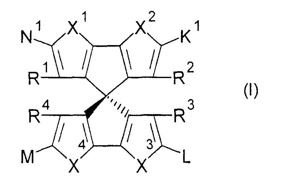
- X1, X2, X3, X4
- sind gleich oder verschieden -S-, -O-, -NR5-, -CR5=N-, -CR5=CH-, mit der Maßgabe, daß mindestens eine der Gruppen X1-4 von -CR5=CH- verschieden ist;
- K1, L, M, N1, R1, R2, R3, R4
- sind gleich oder verschieden und bedeuten
- a) Wasserstoff, -NO2, -CN, -F oder -Cl,
- b) ein geradkettiger oder verzweigter Alkylrest mit 1 bis 20 C-Atomen, wobei
- b1 ) eine oder mehrere nicht benachbarte CH2-Gruppen durch -O-, -S-, - CO-O-, -O-CO-, -O-CO-O-, NR5 oder -Si(CH3)2- ersetzt sein können und/oder
- b2) eine oder mehrere CH2-Gruppen durch -CH=CH-, -C≡C-, 1,4-Phenylen, 1,4-Cyclohexylen oder 1,3-Cyclopentylen ersetzt sein können und/oder
- b3) ein oder mehrere H-Atome durch F und/oder Cl ersetzt sein können und/oder
- c) eine der folgenden Gruppen:
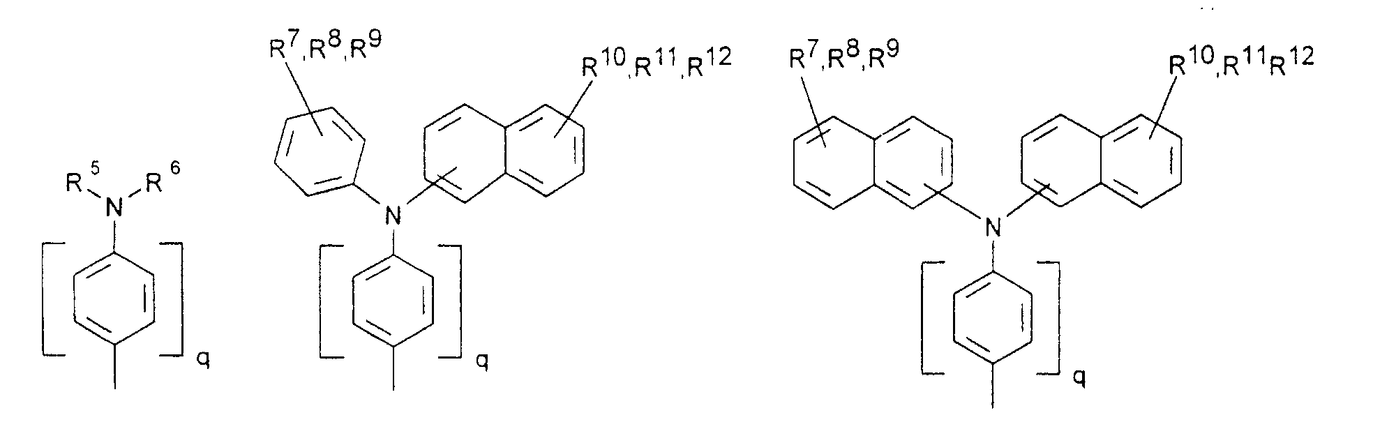

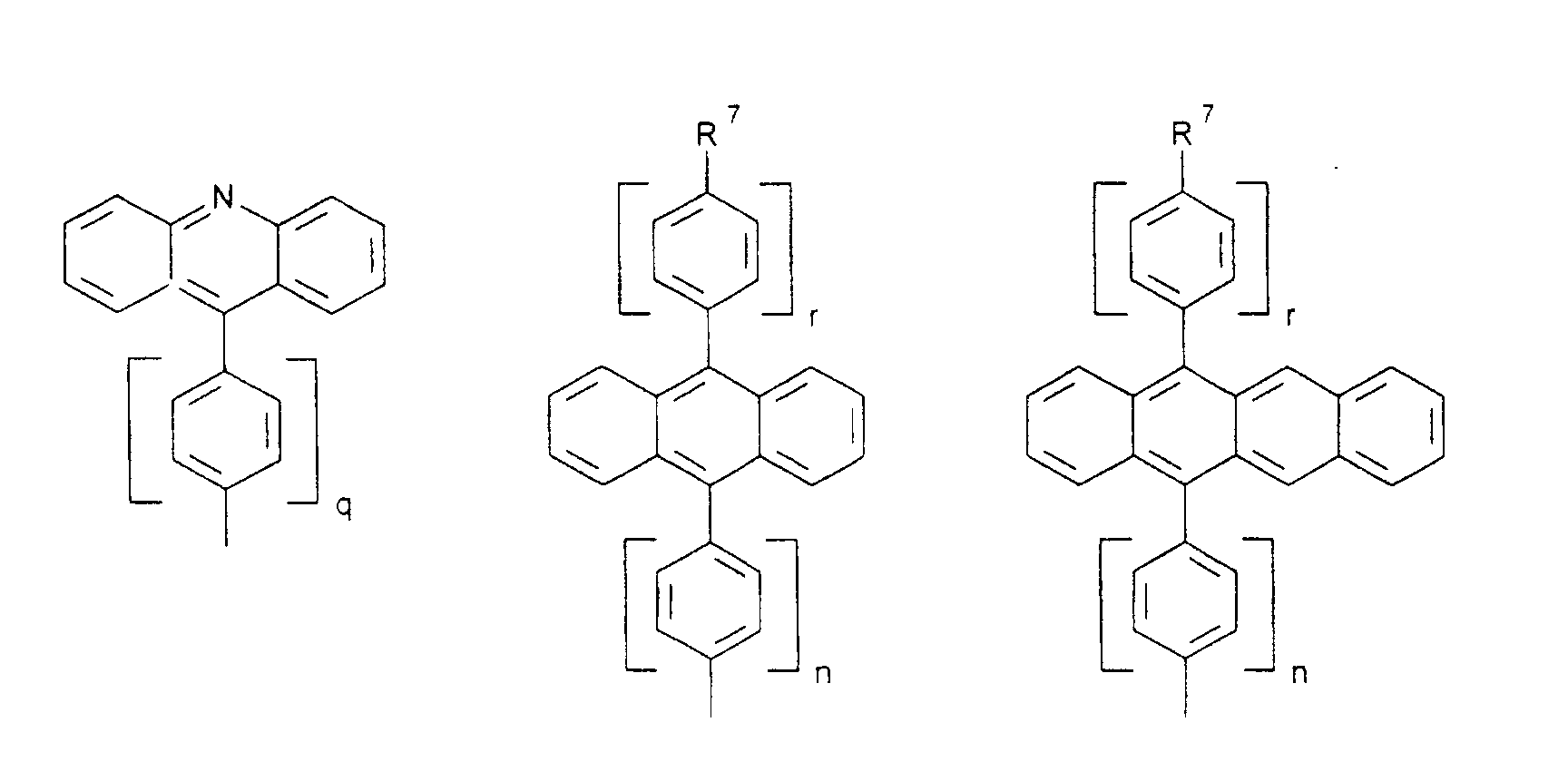 oder
oder
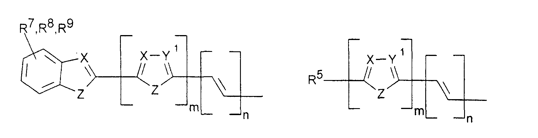

- X, Y1
- sind jeweils gleich oder verschieden =CR7- oder =N-;
- Z
- ist -O-, -S-, -NR5-;
- R5, R6
- sind jeweils gleich oder verschieden
- a) Wasserstoff
- b) ein geradkettiger oder verzweigter Alkylrest mit 1 bis 20 C-Atomen,
wobei
- b1 ) eine oder mehrere nicht benachbarte und nicht an Stickstoff gebundene CH2-Gruppen durch -O-, -S-, -CO-O-, -O-CO-, -O-CO-O- oder -Si(CH3)2 ersetzt sein können und/oder
- b2) eine oder mehrere CH2-Gruppen durch -CH=CH-, -C≡C-, Cyclopropan-1,2-diyl, 1,4-Phenylen, 1,4-Cyclohexylen oder 1,3-Cyclopentylen ersetzt sein können und/oder
- b3) ein oder mehrere H-Atome durch F und/oder Cl ersetzt sein können und/oder
- b4) R5 und R6 zusammen auch einen Ring bilden können;
- c) Phenyl, Biphenyl, 1-Naphthyl, 2-Naphthyl, 2-Thienyl, 2-Furanyl;
- R7, R8, R9, R10, R11, R12
- sind gleich oder verschieden
- a) Wasserstoff, -CN, -F, NO2 oder -Cl
- b) ein geradkettiger oder verzweigter Alkylrest mit 1 bis 20 C-Atomen,
wobei
- b1) eine oder mehrere nicht benachbarte CH2-Gruppen durch -O-, - S-, -CO-O-, -O-CO-, -O-CO-O-, -NR5 oder -Si(CH3)2- ersetzt sein können und/oder
- b2) eine oder mehrere CH2-Gruppen durch -CH=CH-, -C≡C-, Cyclopropan-1,2-diyl, 1,4-Phenylen, 1,4-Cyclohexylen oder 1,3-Cyclopentylen ersetzt sein können und/oder
- b3) ein oder mehrere H-Atome durch F und/oder Cl ersetzt sein können;
- c) Phenyl, Biphenyl, 1-Naphthyl, 2-Naphthyl, 2-Thienyl, 2-Furanyl, -O-Phenyl, -O-Biphenyl, -O-1-Naphthyl, -O-2-Naphthyl, -O-2-Thienyl, -O-2-Furanyl,
- m, n, p, q, r
- sind jeweils gleich oder verschieden 0, 1, 2, 3, 4, 5 oder 6, vorzugsweise 0, 1, 2, 3, 4, 5 oder 6, vorzugsweise 0, 1, 2, 3, 4, besonders bevorzugt 0, 1, 2 oder 3,


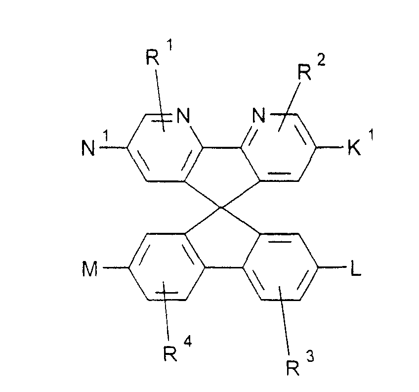
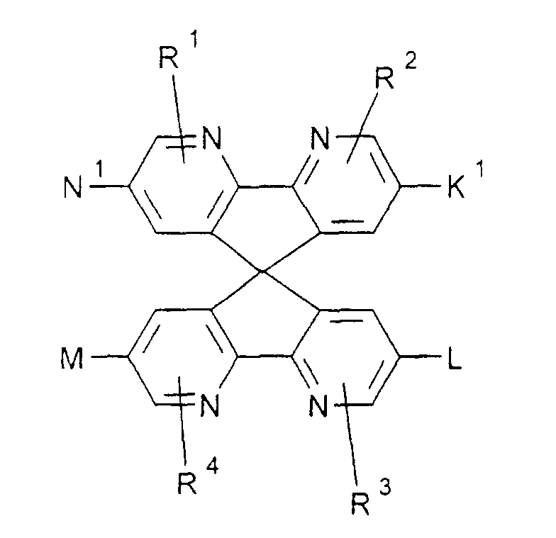
wobei die Symbole folgende Bedeutungen haben:


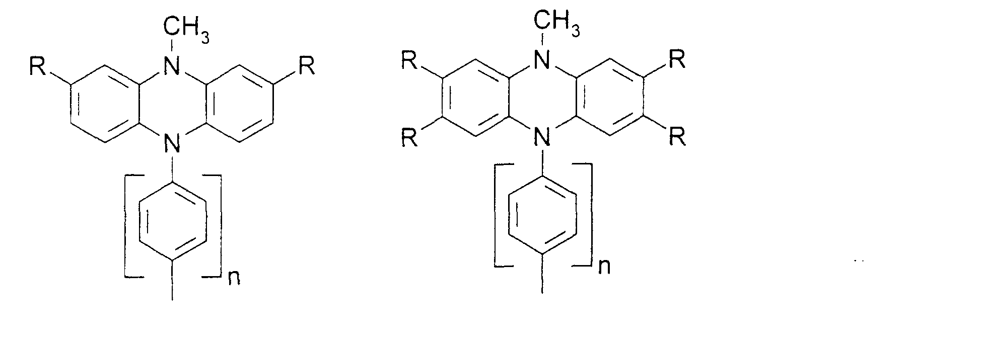


- R
- gleich oder verschieden H, Alkyl, -O-Alkyl, -S-Alkyl, mit jeweils 1 bis 20 C-Atomen, vorzugsweise 1 bis 4 C-Atomen, Phenyl, Biphenyl, 1-Naphthyl, 2-Naphthyl, 2-Thienyl, 2-Furanyl, -O-Phenyl, -O-Biphenyl, -O-1-Naphthyl, -O-2-Naphthyl, -O-2-Thienyl, -O-2-Furanyl, CN, NR2, wobei -O-Alkyl/Aryl, -S-Alkyl/Aryl, CN, NR2 nicht an Stickstoff gebunden sein darf;
- n
- = 0,1,2,3,4.
H, COOR, CH2OR,


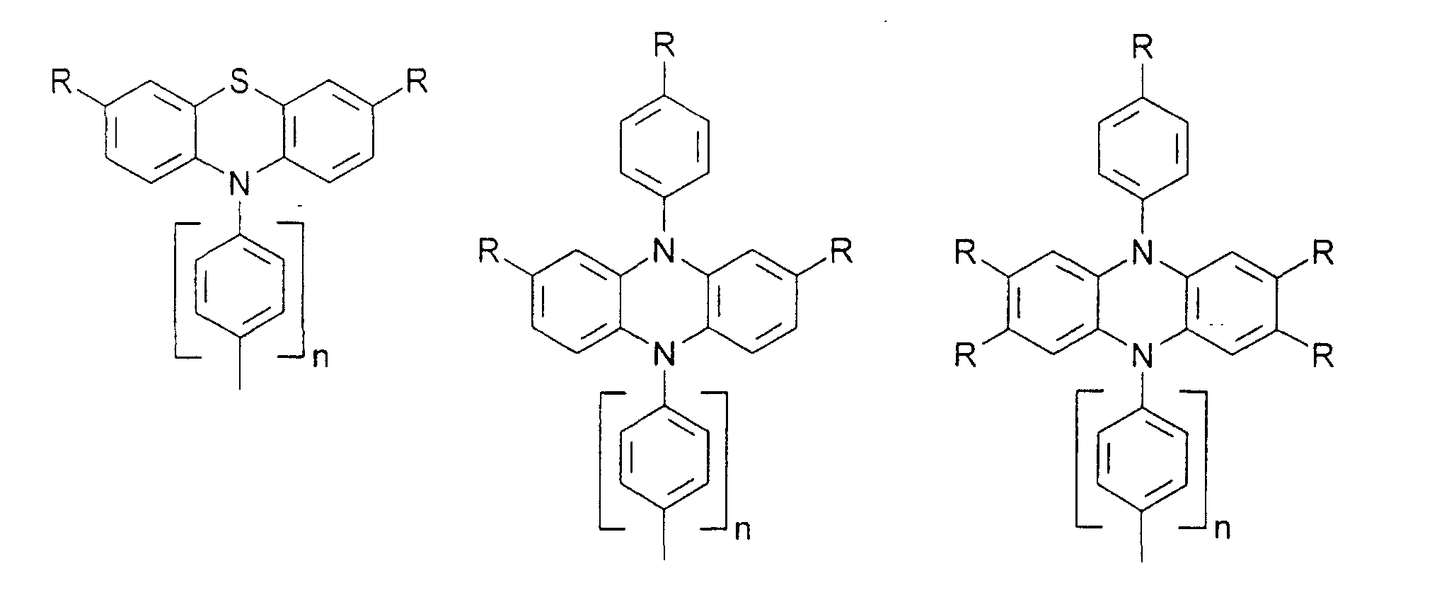
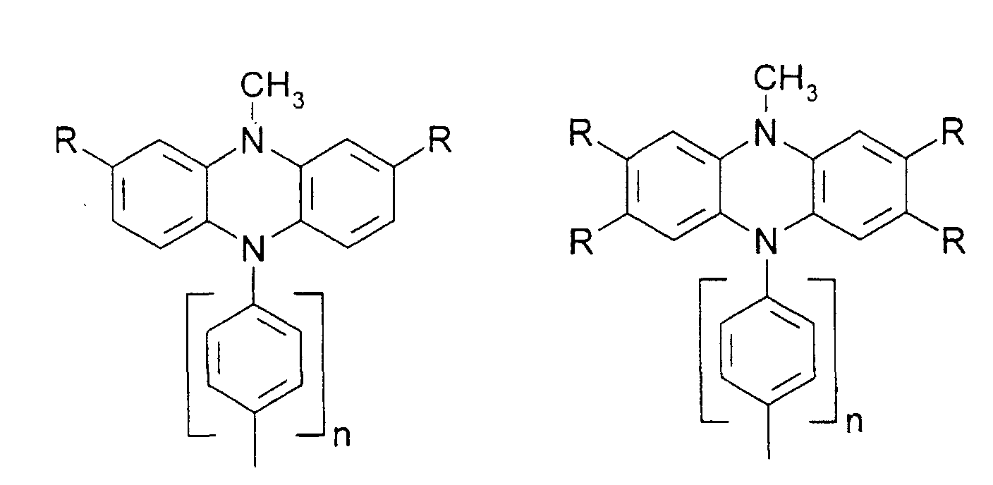
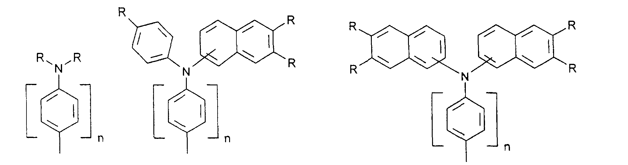


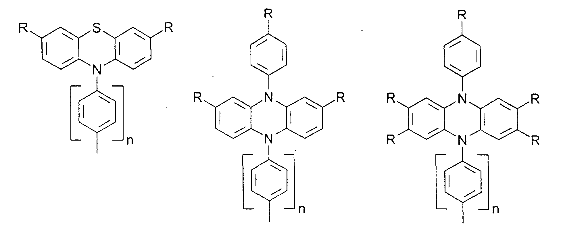


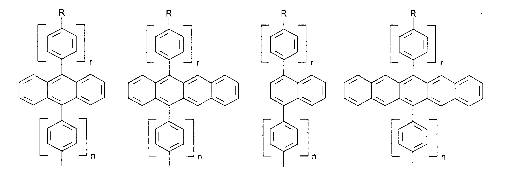
H, COOR, CH2OR,




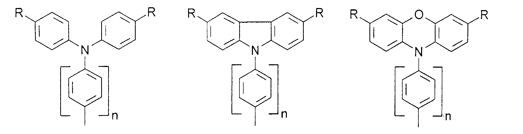
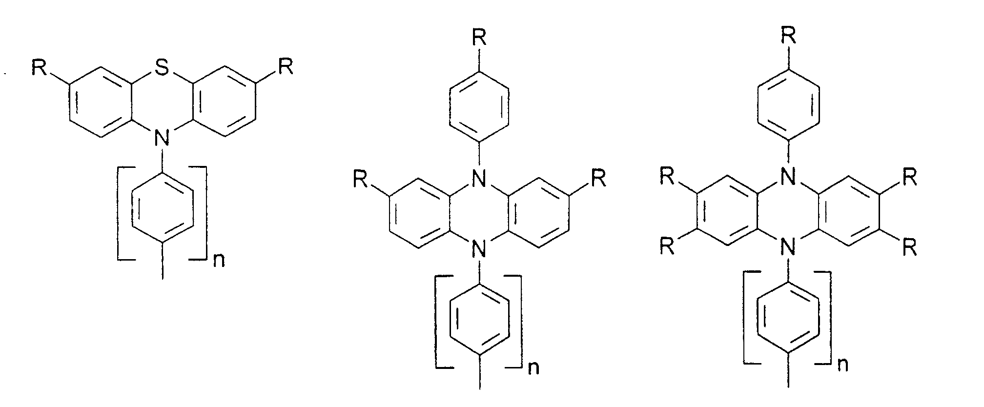
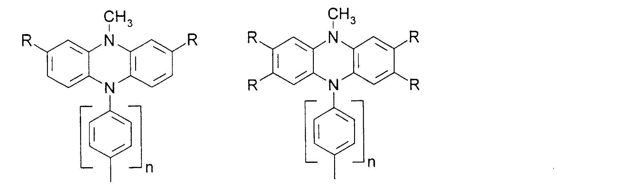
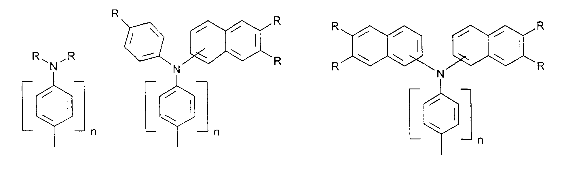





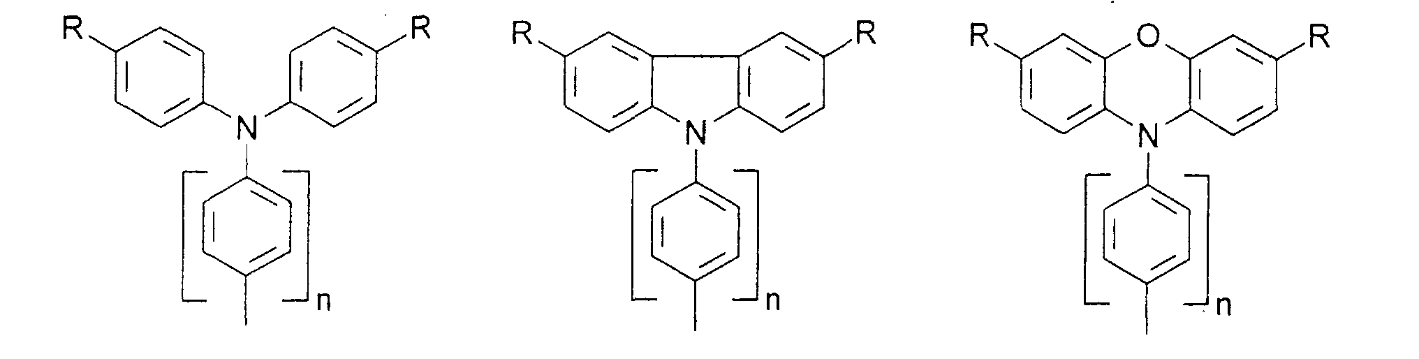
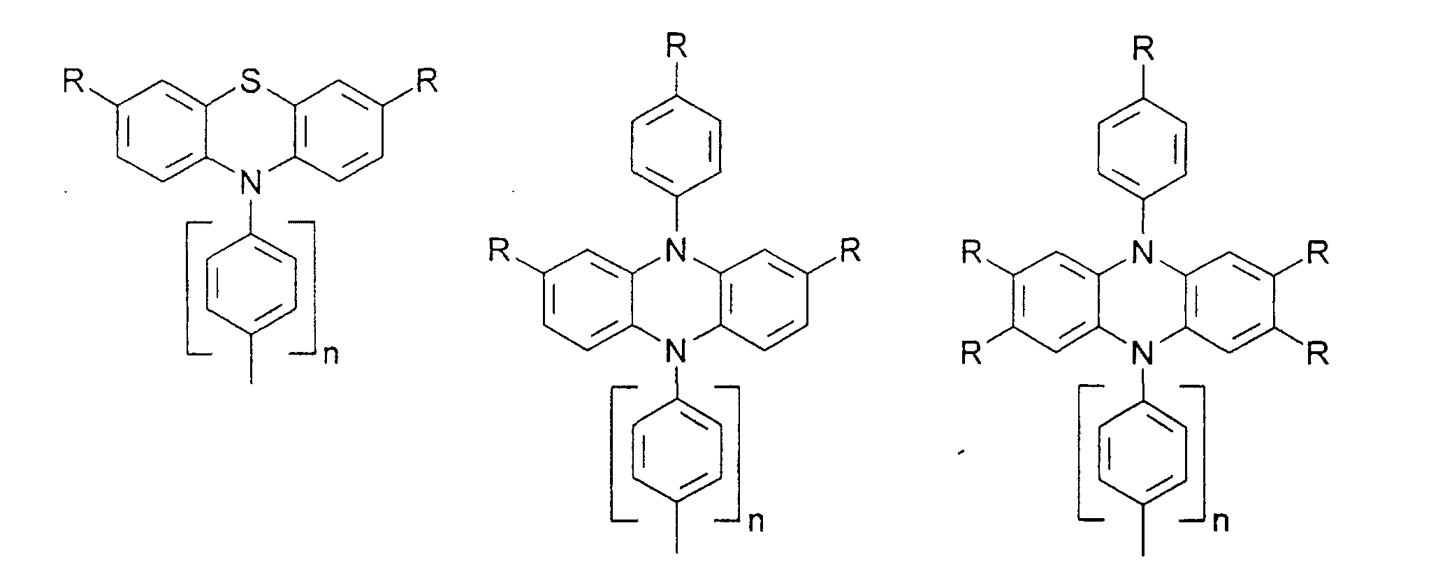


H, COOR, CH2OR,





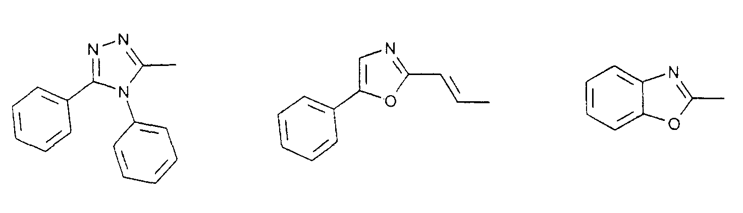
wobei vorzugsweise mindestens zwei der Reste R1-4 H sind.
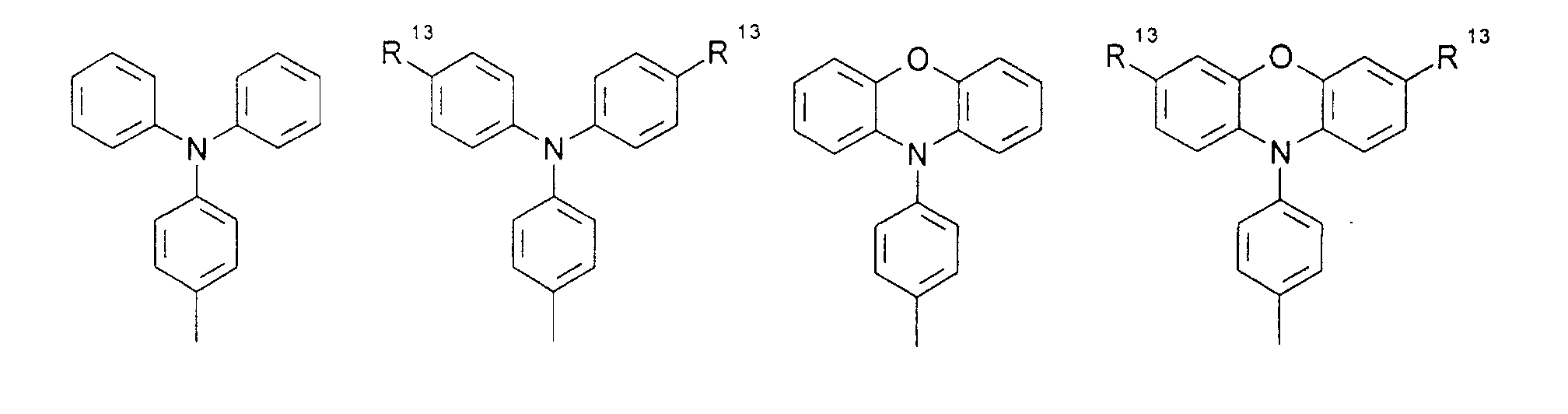
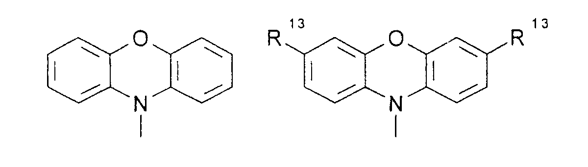


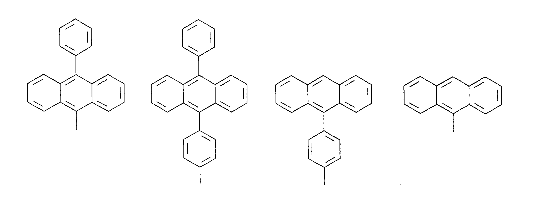
besonders bevorzugt -O-CH3, bedeutet;
und R1=R2=R3=R4 und ist aus der Gruppe
H, COOR14, CH2OR14,


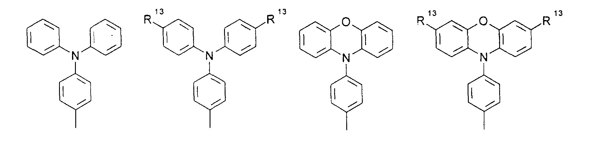



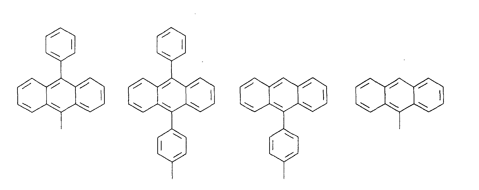
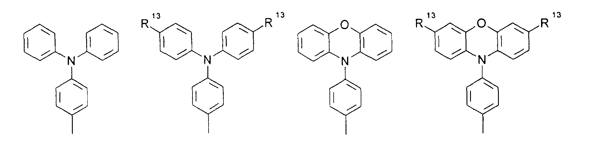

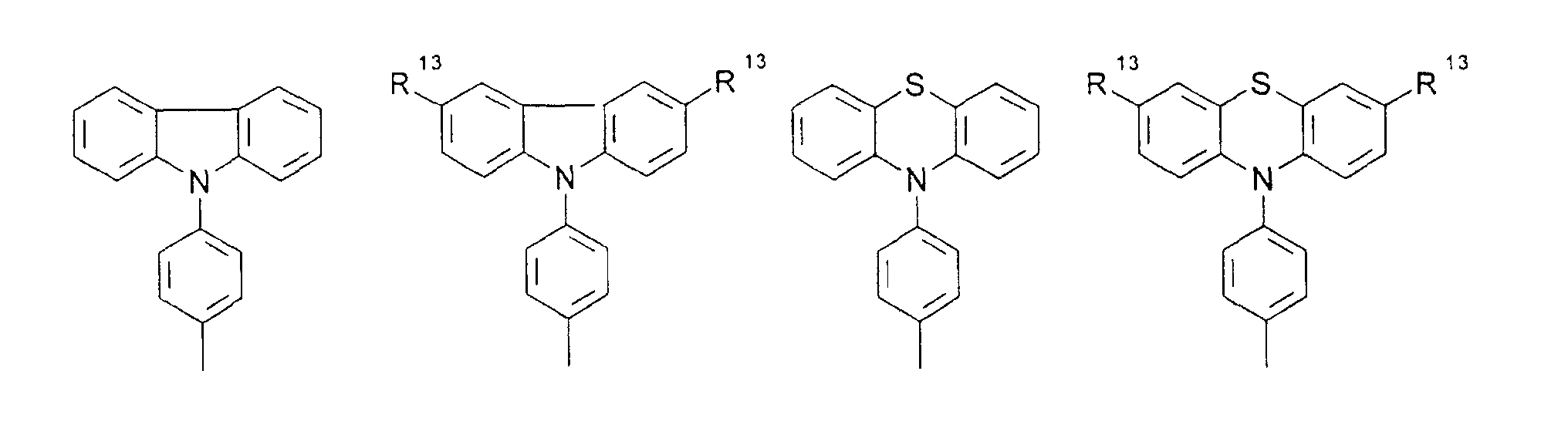

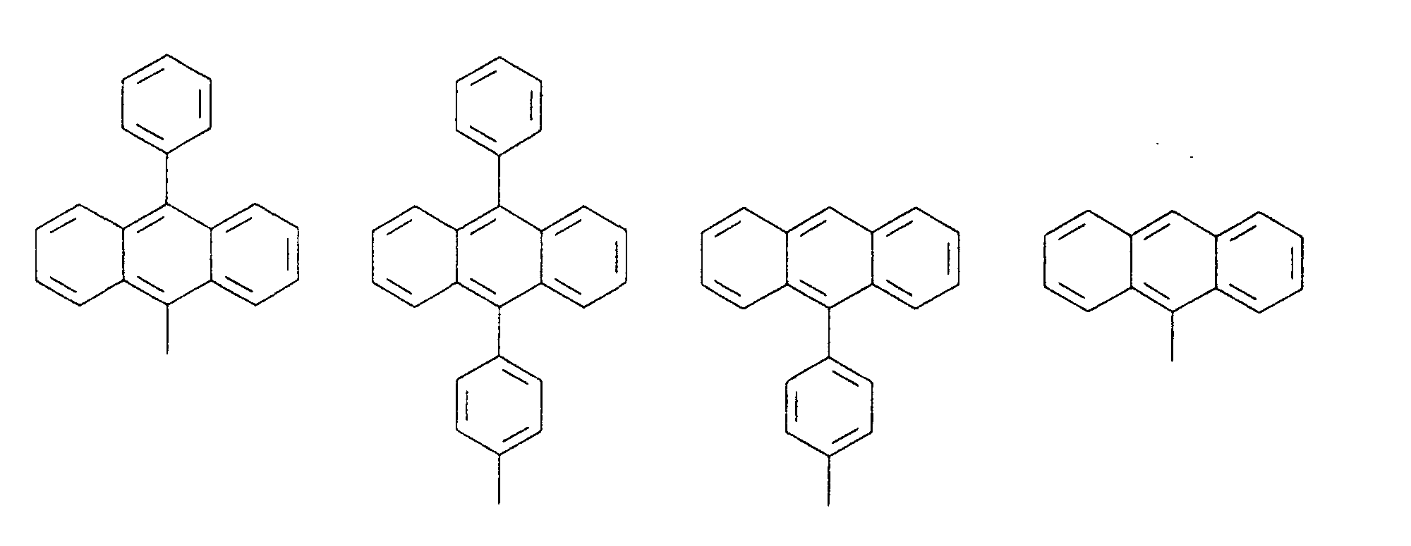
H, COOR14, CH2OR14,


Auf einem leitenden Träger 11, der als Elektrode bzw. Kontakt dienen kann und beispielsweise aus einem Metall oder Indium-Zinn-Oxid (ITO) besteht, ist als lichtabsorbierende Schicht ein Halbleiter 12 aufgebracht, der vorzugsweise eine Oberfläche mit einem Rauheitsfaktor > 1 hat. Vorzugsweise enthält die erfindungsgemäße Zelle auf der Oberfläche des Halbleiters einen Chromophor, hier als Chromophorschicht 13 dargestellt. Die Bezeichnung lichtabsorbierende Schicht umfaßt im Sinne der Erfindung sowohl eine Halbleiterschicht als auch eine Kombination Halbleiter/Chromophor, auch wenn die eigentliche Absorption in diesem Fall nahezu ausschließlich durch den Chromophor erfolgt. Daran schließt sich die Ladungstransportschicht 14 an, die erfindungsgemäß eine Spiroverbindung der Formel (I) enthält. Sie wird auf der einen Seite durch die Gegenelektrode 15 begrenzt, die beispielsweise aus einem leitfähigen Glas, leitfähig beschichtetem Kunststoff, aus Metall oder einem anderen leitfähigen, vorzugsweise lichtdurchlässigen Material, bestehen kann. Die Zelle 1 ist vorzugsweise oben und unten durch je eine isolierende Schicht 16 bzw. 17 abgeschlossen. Sie kann einen, in der Figur nicht gezeigten seitlichen Abschluß enthalten, beispielsweise einen Rahmen aus einem elektrisch isolierendem Material, wie Kunststoff oder Glas. Durch die Verwendung eines Lochleitermaterials anstelle des flüssigen Elektrolyten ist solch ein seitlicher Rahmen aber nicht grundsätzlich notwendig. Zumindest eine Seite der Zelle muß für das in elektrische Energie zu wandelnde Licht durchlässig sein, so daß dieses zu dem Chromophor bzw. dem Halbleiter gelangen kann.
Die Zelle enthält darüber hinaus in der Figur nicht gezeigte Vorrichtungen zur Abnahme des von der Zelle erzeugten elektrischen Stroms.
Damit eignen sich vorzugsweise Metalloxid-Halbleiter, insbesondere die Oxyde der Übergangsmetalle, sowie der Elemente der dritten Hauptgruppe und der vierten, fünften und sechsten Nebengruppe (des periodischen Systems der Elemente) von Titan, Zirkon, Hafnium, Strontium, Zink, Indium, Yttrium, Lanthan, Vanadium, Niob, Tantal, Chrom, Molybdän, Wolfram, aber auch Oxide von Zink, Eisen, Nickel oder Silber, Perovskite wie SrTiO3, CaTiO3, oder Oxide von anderen Metallen der zweiten und dritten Hauptgruppe oder Mischoxide oder Oxidgemische dieser Metalle. Es kann aber auch jedes andere Metalloxid mit Halbleitereigenschaften und großem Energieabstand (Bandlücke) zwischen Valenzband und Leitungband verwendet werden.
Besonders bevorzugt als Halbleitermaterial ist Titandioxid.
Der Rauheitsfaktor ist definiert als das Verhältnis einer wirklichen/effektiven Oberfläche zur Fläche der Projektion dieser Oberfläche eines Körpers, in diesem Fall also der Oberfläche des Halbleiters.
S. 397 (Stuttgart: B.G. Teubner, 1985) beschrieben wird. Im allgemeinen beträgt die Größe der Poren 5-200 nm, vorzugsweise 10-50 nm.
Die rauhe Oberfläche mit polykristalliner Struktur bietet eine um den Rauheitsfaktor größere Fläche für eine, vorzugsweise, monomolekulare Oberflächenschicht eines Chromophors. Damit wird erreicht, daß das auf eine Fläche bestimmter Größe einfallende Licht mit bedeutend höherer Ausbeute in elektrische Energie gewandelt wird. Der Halbleiter kann als für den einfallenden Lichtstrom durchsichtig betrachtet werden. Licht wird aber teilweise auf der Oberfläche reflektiert und gelangt z. T. auf benachbarte Oberflächen. Das in den Halbleiter eindringende und nicht absorbierte bzw. gewandelte Licht trifft z. T. direkt und zu einem anderen Teil indirekt und zu einem weiteren Teil indirekt nach Totalreflexion an der Oberfläche, auf der Austrittsseite auf Chromophormoleküle, womit es gelingt, eine bedeutend höhere Lichtausbeute zu erzielen.
Verschiedene Chromophore haben unterschiedliche spektrale Empfindlichkeiten. Die Wahl des Chromophors kann somit der spektralen Zusammensetzung des Lichts der Lichtquelle angepaßt werden, um die Ausbeute möglichst zu vergrößern. Als Chromophore, d. h. Sensibilisatoren, eigenen sich insbesondere die Komplexe von Übergangsmetallen vom Typ Metall (L3), Metall (L2) von Ruthenium und Osmium (z. B. Ruthenium-tris-(2,2'-bipyridyl-4,4'-dicarbonsäure) und deren Salze, Ruthenium cis diaqua bipyridyl Komplexe, wie Ruthenium cis-diaqua bis(2,2'bipyridyl-4,4'dicarboxylate) sowie Porphyrine (z. B. Zink tetra (4-carboxyphenyl) Porphyrin) und Cyanide (z. B. Eisen-Hexacyanid-Komplexe) und Phthalocyanine.
Die Chromophore können im Bereich der Oberfläche des Metalloxyd-Halbleiters chemisorbiert, adsorbiert oder sonstwie fest angelagert sein. Günstige Resultate wurden beispielsweise mit Chromophoren erzielt, die mit Carbonsäure- oder Phosphonsäure-Liganden an die Oberfläche des Metalloxyd-Halbleiters gebunden sind.


Sie kann zur Vermeidung von Reflexionsverlusten mit einer ein-, zwei- oder mehrlagigen Antireflexschicht versehen sein.
Die Farbe des emittierten Lichtes kann durch die als lichtemittierende Schicht verwendeten Materialien variiert werden.
Claims (5)
- Spiroverbindungen der allgemeinen Formel (I),wobei die Symbole folgende Bedeutungen haben:

- X1, X2, X3, X4
- sind gleich oder verschieden -S-, -O-, -NR5-, -CR5=N-, -CR5=CH-, mit der Maßgabe, daß mindestens eine der Gruppen X1-4 von -CR5=CH- verschieden ist;
- K1, L, M, N1, R1, R2, R3, R4
- sind gleich oder verschieden und bedeuten
- a) Wasserstoff, -NO2, -CN, -F oder -Cl,
- b) ein geradkettiger oder verzweigter Alkylrest mit 1 bis 20 C-Atomen, wobei
- b1 ) eine oder mehrere nicht benachbarte CH2-Gruppen durch -O-, -S-, -CO-O-, -O-CO-, -O-CO-O-, NR5 oder -Si(CH3)2- ersetzt sein können und/oder
- b2) eine oder mehrere CH2-Gruppen durch -CH=CH-, -C≡C-, 1,4-Phenylen, 1,4-Cyclohexylen oder 1,3-Cyclopentylen ersetzt sein können und/oder
- b3) ein oder mehrere H-Atome durch F und/oder Cl ersetzt sein können und/oder
- c) eine der folgenden Gruppen:
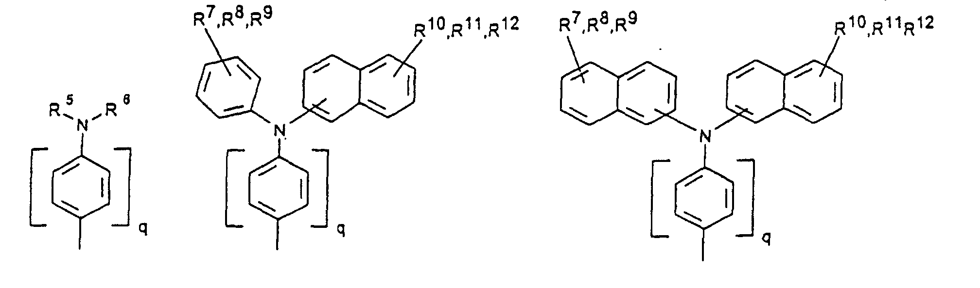

 oder
oder


- X, Y1
- sind jeweils gleich oder verschieden =CR7- oder =N-;
- Z
- ist -O-, -S-, =NR5-,
- R5, R6
- sind jeweils gleich oder verschieden
- a) Wasserstoff
- b) ein geradkettiger oder verzweigter Alkylrest mit 1 bis 20 C-Atomen,
wobei
- b1 ) eine oder mehrere nicht benachbarte und nicht an Stickstoff gebundene CH2-Gruppen durch -O-, -S-, -CO-O-, -O-CO-, -O-CO-O- oder -Si(CH3)2 ersetzt sein können und/oder
- b2) eine oder mehrere CH2-Gruppen durch -CH=CH-, -C≡C-, Cyclopropan-1,2-diyl, 1,4-Phenylen, 1,4-Cyclohexylen oder 1,3-Cyclopentylen ersetzt sein können und/oder
- b3) ein oder mehrere H-Atome durch F und/oder Cl ersetzt sein können und/oder
- b4) R5 und R6 zusammen auch einen Ring bilden können;
- c) Phenyl, Biphenyl, 1-Naphthyl, 2-Naphthyl, 2-Thienyl, 2-Furanyl;
- R7, R8, R9, R10, R11, R12
- sind gleich oder verschieden
- a) Wasserstoff, -CN, -F, NO2 oder -Cl
- b) ein geradkettiger oder verzweigter Alkylrest mit 1 bis 20 C-Atomen,
wobei - b1 ) eine oder mehrere nicht benachbarte CH2-Gruppen durch -O-, -S-, -CO-O-, -O-CO-, -O-CO-O-, -NR5 oder -Si(CH3)2- ersetzt sein können und/oder
- b2) eine oder mehrere CH2-Gruppen durch -CH=CH-, -C≡C-, Cyclopropan-1,2-diyl, 1,4-Phenylen, 1,4-Cyclohexylen oder 1,3-Cyclopentylen ersetzt sein können und/oder
- b3) ein oder mehrere H-Atome durch F und/oder Cl ersetzt sein können;
- c) Phenyl, Biphenyl, 1-Naphthyl, 2-Naphthyl, 2-Thienyl, 2-Furanyl, -O-Phenyl, -O-Biphenyl, -O-1-Naphthyl, -O-2-Naphthyl, -O-2-Thienyl, -O-2-Furanyl,
- m, n, p, q, r
- sind jeweils gleich oder verschieden 0, 1, 2, 3, 4, 5 oder 6,
sowie 4,5-Diazospirobifluoren und 4,4',5,5'-Tetraazospirobifluoren.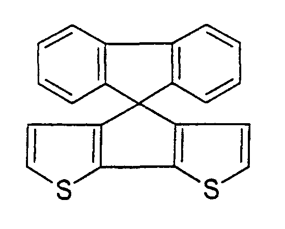
- Spiroverbindungen gemäß Formel (1) in Anspruch 1, dadurch gekennzeichnet, daß:a) X1-4 identisch sind oderb) X1 gleich X2 und X3 gleich X4 ist.
- Spiroverbindungen gemäß Anspruch 1 und/oder 2, aus der Gruppea)
 b)
b)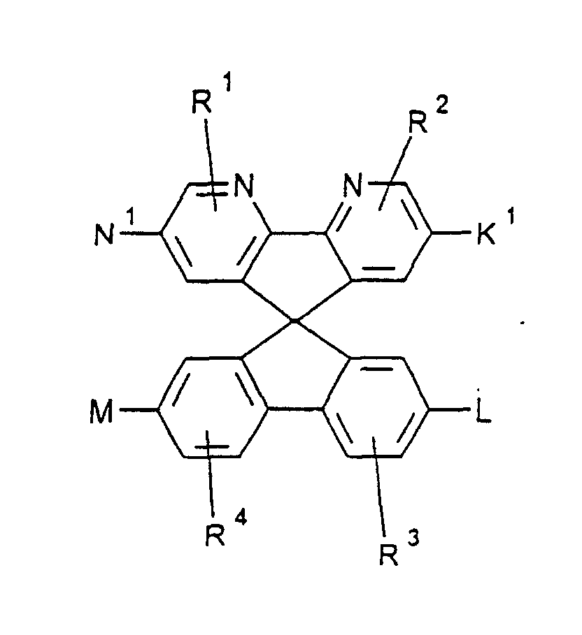 c)
c)
- Verwendung einer amorphen Spiroverbindung der allgemeinen Formel (I)wobei die Symbole folgende Bedeutungen haben:

- X1, X2, X3, X4
- sind gleich oder verschieden -S-, -O-, -NR5-, -CR5=N-, -CR5=CH-, mit der Maßgabe, daß mindestens eine der Gruppen X1-4 von -CR5=CH- verschieden ist;
- K1, L, M, N1, R1, R2, R3, R4
- sind gleich oder verschieden und bedeuten
- a) Wasserstoff, -NO2, -CN, -F oder -Cl,
- b) ein geradkettiger oder verzweigter Alkylrest mit 1 bis 20 C-Atomen, wobei
- b1) eine oder mehrere nicht benachbarte CH2-Gruppen durch -O-, -S-, -CO-O-, -O-CO-, -O-CO-O-, NR5 oder -Si(CH3)2- ersetzt sein können und/oder
- b2) eine oder mehrere CH2-Gruppen durch -CH=CH-, -C≡C-, 1,4-Phenylen, 1,4-Cyclohexylen oder 1,3-Cyclopentylen ersetzt sein können und/oder
- b3) ein oder mehrere H-Atome durch F und/oder Cl ersetzt sein können und/oder
- c) eine der folgenden Gruppen:
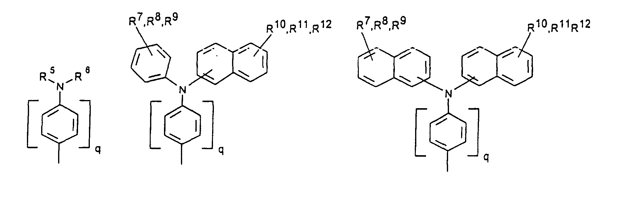
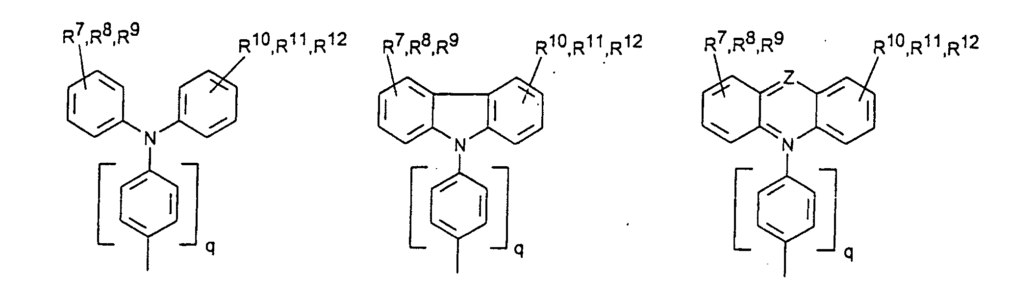
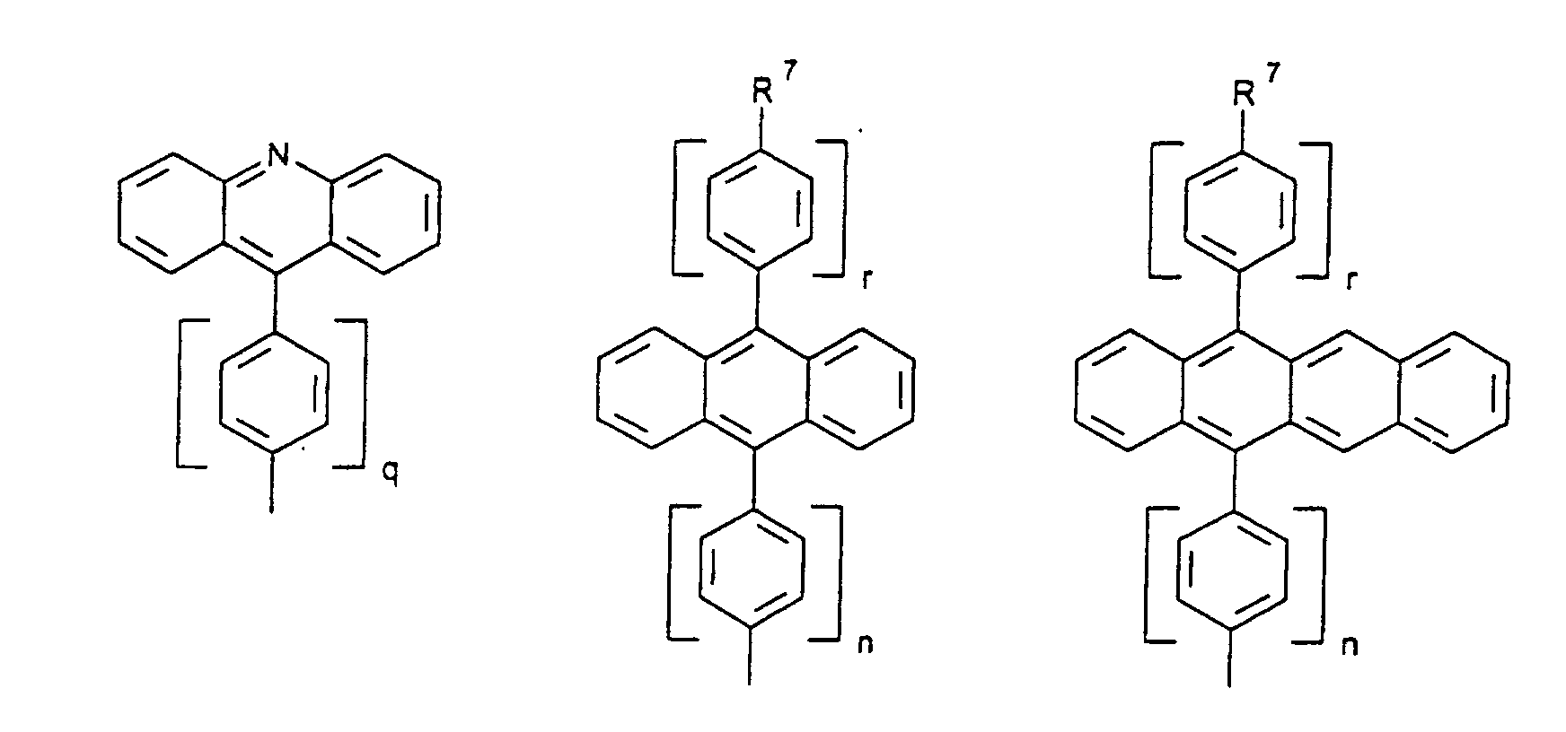 oder
oder
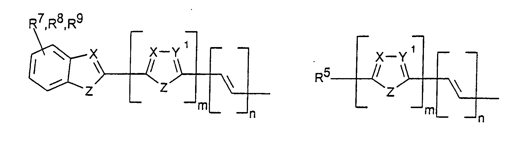

- X, Y1
- sind jeweils gleich oder verschieden =CR7- oder =N-;
- Z
- ist -O-, -S-, -NR5-,
- R5, R6
- sind jeweils gleich oder verschieden
- a) Wasserstoff
- b) ein geradkettiger oder verzweigter Alkylrest mit 1 bis 20 C-Atomen,
wobei
- b1 ) eine oder mehrere nicht benachbarte und nicht an Stickstoff gebundene CH2-Gruppen durch -O-, -S-, -CO-O-, -O-CO-, -O-CO-O- oder -Si(CH3)2 ersetzt sein können und/oder
- b2) eine oder mehrere CH2-Gruppen durch -CH=CH-, -C≡C-, Cyclopropan-1,2-diyl, 1,4-Phenylen, 1,4-Cyclohexylen oder 1,3-Cyclopentylen ersetzt sein können und/oder
- b3) ein oder mehrere H-Atome durch F und/oder Cl ersetzt sein können und/oder
- b4) R5 und R6 zusammen auch einen Ring bilden können;
- c) Phenyl, Biphenyl, 1-Naphthyl, 2-Naphthyl, 2-Thienyl, 2-Furanyl;
- R7, R8, R9, R10, R11, R12
- sind gleich oder verschieden
- a) Wasserstoff, -CN, -F, NO2 oder -Cl
- b) ein geradkettiger oder verzweigter Alkylrest mit 1 bis 20 C-Atomen,
wobei
- b1 ) eine oder mehrere nicht benachbarte CH2-Gruppen durch -O-, -S-, -CO-O-, -O-CO-, -O-CO-O-, -NR5 oder -Si(CH3)2- ersetzt sein können und/oder
- b2) eine oder mehrere CH2-Gruppen durch -CH=CH-, -C≡C-, Cyclopropan-1,2-diyl, 1,4-Phenylen, 1,4-Cyclohexylen oder 1,3-Cyclopentylen ersetzt sein können und/oder
- b3) ein oder mehrere H-Atome durch F und/oder Cl ersetzt sein können;
- c) Phenyl, Biphenyl, 1-Naphthyl, 2-Naphthyl, 2-Thienyl, 2-Furanyl, -O-Phenyl, -O-Biphenyl, -O-1-Naphthyl, -O-2-Naphthyl, -O-2-Thienyl, -O-2-Furanyl,
- m, n, p, q, r
- sind jeweils gleich oder verschieden 0, 1, 2, 3, 4, 5 oder 6.
- Photovoltaische Zelle, enthaltend eine Ladungstransportschicht, die eine oder mehrere Spiroverbindungen gemäß Anspruch 4 enthält.
Applications Claiming Priority (3)
| Application Number | Priority Date | Filing Date | Title |
|---|---|---|---|
| DE19711568 | 1997-03-20 | ||
| DE19711568A DE19711568A1 (de) | 1997-03-20 | 1997-03-20 | Spiroverbindungen und deren Verwendung |
| PCT/EP1998/001589 WO1998042715A1 (de) | 1997-03-20 | 1998-03-18 | Spiroverbindungen und deren verwendung |
Publications (2)
| Publication Number | Publication Date |
|---|---|
| EP0970086A1 EP0970086A1 (de) | 2000-01-12 |
| EP0970086B1 true EP0970086B1 (de) | 2003-12-10 |
Family
ID=7823978
Family Applications (1)
| Application Number | Title | Priority Date | Filing Date |
|---|---|---|---|
| EP98913731A Expired - Lifetime EP0970086B1 (de) | 1997-03-20 | 1998-03-18 | Spiroverbindungen und deren verwendung |
Country Status (5)
| Country | Link |
|---|---|
| US (1) | US6211369B1 (de) |
| EP (1) | EP0970086B1 (de) |
| JP (1) | JP4278185B2 (de) |
| DE (2) | DE19711568A1 (de) |
| WO (1) | WO1998042715A1 (de) |
Families Citing this family (15)
| Publication number | Priority date | Publication date | Assignee | Title |
|---|---|---|---|---|
| DE19711714A1 (de) * | 1997-03-20 | 1998-10-01 | Hoechst Ag | Spiroverbindungen und deren Verwendung |
| US6656608B1 (en) * | 1998-12-25 | 2003-12-02 | Konica Corporation | Electroluminescent material, electroluminescent element and color conversion filter |
| KR100377575B1 (ko) * | 2000-10-17 | 2003-03-26 | 삼성에스디아이 주식회사 | 유기 전계 발광 소자용 청색 발광 화합물 및 이를 사용한유기 전계 발광 소자 |
| JP3669333B2 (ja) * | 2001-02-06 | 2005-07-06 | ソニー株式会社 | 有機電界発光素子及び表示装置 |
| US6998487B2 (en) * | 2001-04-27 | 2006-02-14 | Lg Chem, Ltd. | Double-spiro organic compounds and organic electroluminescent devices using the same |
| WO2003008475A2 (en) * | 2001-07-20 | 2003-01-30 | University Of Rochester | Light-emitting organic oligomer compositions |
| ITRM20020411A1 (it) * | 2002-08-01 | 2004-02-02 | Univ Roma La Sapienza | Derivati dello spirobifluorene, loro preparazione e loro uso. |
| US7014925B2 (en) * | 2003-04-29 | 2006-03-21 | Canon Kabushiki Kaisha | Heterogeneous spiro compounds in organic light emitting device elements |
| DE102004021989A1 (de) * | 2004-05-04 | 2005-12-15 | Covion Organic Semiconductors Gmbh | Organische elektronische Vorrichtungen |
| KR100669790B1 (ko) * | 2004-11-27 | 2007-01-16 | 삼성에스디아이 주식회사 | 유기 전계 발광 소자 |
| US20070116984A1 (en) * | 2005-09-21 | 2007-05-24 | Doosan Corporation | Spiro-compound for electroluminescent display device and electroluminescent display device comprising the same |
| KR100798817B1 (ko) | 2006-07-28 | 2008-01-28 | 주식회사 두산 | 전계 발광 소자용 스피로 화합물, 및 이를 포함하는 전계발광 소자 |
| TWI394309B (zh) * | 2009-12-30 | 2013-04-21 | Ind Tech Res Inst | 染料敏化太陽能電池 |
| CN106831777A (zh) * | 2016-12-16 | 2017-06-13 | 吴中区穹窿山天仲高分子材料技术研究所 | 一种新型oled材料 |
| CN118047792A (zh) * | 2024-03-13 | 2024-05-17 | 天合光能股份有限公司 | 有机化合物及其制备方法、应用、太阳能电池及其制备方法 |
Family Cites Families (6)
| Publication number | Priority date | Publication date | Assignee | Title |
|---|---|---|---|---|
| CH674596A5 (de) | 1988-02-12 | 1990-06-15 | Sulzer Ag | |
| EP0676461B1 (de) | 1994-04-07 | 2002-08-14 | Covion Organic Semiconductors GmbH | Spiroverbindungen und ihre Verwendung als Elektrolumineszenzmaterialien |
| DE4445584A1 (de) | 1994-12-20 | 1996-06-27 | Basf Ag | Verwendung von organischen Materialien hoher nichtionischer Ladungsträgerbeweglichkeit |
| JPH0918039A (ja) * | 1995-06-30 | 1997-01-17 | Nippon Shokubai Co Ltd | 有機太陽電池 |
| DE19533850A1 (de) | 1995-09-13 | 1997-03-27 | Hoechst Ag | Photovoltaische Zelle |
| DE19614971A1 (de) * | 1996-04-17 | 1997-10-23 | Hoechst Ag | Polymere mit Spiroatomen und ihre Verwendung als Elektrolumineszenzmaterialien |
-
1997
- 1997-03-20 DE DE19711568A patent/DE19711568A1/de not_active Withdrawn
-
1998
- 1998-03-18 WO PCT/EP1998/001589 patent/WO1998042715A1/de not_active Ceased
- 1998-03-18 JP JP54442198A patent/JP4278185B2/ja not_active Expired - Lifetime
- 1998-03-18 DE DE59810405T patent/DE59810405D1/de not_active Expired - Lifetime
- 1998-03-18 EP EP98913731A patent/EP0970086B1/de not_active Expired - Lifetime
- 1998-03-18 US US09/381,317 patent/US6211369B1/en not_active Expired - Lifetime
Also Published As
| Publication number | Publication date |
|---|---|
| JP2001518914A (ja) | 2001-10-16 |
| US6211369B1 (en) | 2001-04-03 |
| DE19711568A1 (de) | 1998-10-01 |
| EP0970086A1 (de) | 2000-01-12 |
| JP4278185B2 (ja) | 2009-06-10 |
| WO1998042715A1 (de) | 1998-10-01 |
| DE59810405D1 (de) | 2004-01-22 |
Similar Documents
| Publication | Publication Date | Title |
|---|---|---|
| EP0968507B1 (de) | Photovoltaische zelle | |
| EP0968175B1 (de) | Spiroverbindungen und deren verwendung | |
| EP0850492B1 (de) | Photovoltaische zelle mit einer spiroverbindung | |
| DE69526614T2 (de) | Lichtemittierende Vorrichtungen die Organometallische Komplexe enthalten. | |
| DE60108726T2 (de) | Lumineszente polymer | |
| DE69710135T2 (de) | Blauorganische Elektrolumineszenzvorrichtungen | |
| EP1687859B1 (de) | Organisches elektrolumineszenzelement | |
| EP3057151B1 (de) | Wismut- und zinnkomplexe als p-dotanden für organische elektronische matrixmaterialien | |
| DE69938601T2 (de) | Organische elektrolumineszente vorrichtung | |
| DE69627412T2 (de) | Organische elektrolumineszierende Vorrichtungen hoher thermischer Stabilität | |
| DE69027760T2 (de) | Organisches elektrolumineszentes element | |
| DE60306570T2 (de) | Organische elektrolumineszente Vorrichtungen | |
| DE69708997T2 (de) | Elektrotransportmittelmaterialien für organische elektrolumineszente Vorrichtungen | |
| DE69915993T2 (de) | Grüne,organische Elektrolumineszenzvorrichtungen | |
| EP0333641B1 (de) | Photoelektrochemische Zelle, Verfahren zum Herstellen einer derartigen Zelle sowie Verwendung der Zelle | |
| EP2588563B1 (de) | Singulett-harvesting mit organischen molekülen für opto-elektronische vorrichtungen | |
| EP2229699B1 (de) | Dithiolenübergangsmetallkomplexe und elektronische oder optoelektronische bauelemente | |
| EP1668718B1 (de) | Organisches elektrolumineszenzelement | |
| DE19711568A1 (de) | Spiroverbindungen und deren Verwendung | |
| EP0719309A1 (de) | Verwendung von polymeren mit isolierten chromophoren als elektrolumineszenzmaterialien | |
| DE102011013897A1 (de) | Organische Solarzelle | |
| DE10357315A1 (de) | Organisches Elektrolumineszenzelement | |
| EP2318473B1 (de) | Fluorverbrückte assoziate für optoelektronische anwendungen | |
| EP0947006B1 (de) | Strahlungsdetektor | |
| DE102007059887A1 (de) | Lichtemittierendes organisches Bauelement und Verfahren zu dessen Herstellung |
Legal Events
| Date | Code | Title | Description |
|---|---|---|---|
| PUAI | Public reference made under article 153(3) epc to a published international application that has entered the european phase |
Free format text: ORIGINAL CODE: 0009012 |
|
| 17P | Request for examination filed |
Effective date: 19991020 |
|
| AK | Designated contracting states |
Kind code of ref document: A1 Designated state(s): DE FR GB NL |
|
| RAP1 | Party data changed (applicant data changed or rights of an application transferred) |
Owner name: AXIVA GMBH |
|
| RAP1 | Party data changed (applicant data changed or rights of an application transferred) |
Owner name: CELANESE VENTURES GMBH |
|
| 17Q | First examination report despatched |
Effective date: 20011023 |
|
| RAP1 | Party data changed (applicant data changed or rights of an application transferred) |
Owner name: COVION ORGANIC SEMICONDUCTORS GMBH |
|
| GRAH | Despatch of communication of intention to grant a patent |
Free format text: ORIGINAL CODE: EPIDOS IGRA |
|
| GRAS | Grant fee paid |
Free format text: ORIGINAL CODE: EPIDOSNIGR3 |
|
| GRAA | (expected) grant |
Free format text: ORIGINAL CODE: 0009210 |
|
| AK | Designated contracting states |
Kind code of ref document: B1 Designated state(s): DE FR GB NL |
|
| REG | Reference to a national code |
Ref country code: GB Ref legal event code: FG4D Free format text: NOT ENGLISH |
|
| GBT | Gb: translation of ep patent filed (gb section 77(6)(a)/1977) |
Effective date: 20031210 |
|
| REF | Corresponds to: |
Ref document number: 59810405 Country of ref document: DE Date of ref document: 20040122 Kind code of ref document: P |
|
| ET | Fr: translation filed | ||
| PLBE | No opposition filed within time limit |
Free format text: ORIGINAL CODE: 0009261 |
|
| STAA | Information on the status of an ep patent application or granted ep patent |
Free format text: STATUS: NO OPPOSITION FILED WITHIN TIME LIMIT |
|
| 26N | No opposition filed |
Effective date: 20040913 |
|
| REG | Reference to a national code |
Ref country code: GB Ref legal event code: 732E |
|
| NLS | Nl: assignments of ep-patents |
Owner name: MERCK PATENT GMBH Effective date: 20070724 Owner name: MERCK KOMMANDITGESELLSCHAFT AUF AKTIEN Effective date: 20070724 |
|
| NLT1 | Nl: modifications of names registered in virtue of documents presented to the patent office pursuant to art. 16 a, paragraph 1 |
Owner name: MERCK OLED MATERIALS GMBH |
|
| REG | Reference to a national code |
Ref country code: FR Ref legal event code: TP |
|
| PGFP | Annual fee paid to national office [announced via postgrant information from national office to epo] |
Ref country code: FR Payment date: 20100324 Year of fee payment: 13 |
|
| PGFP | Annual fee paid to national office [announced via postgrant information from national office to epo] |
Ref country code: GB Payment date: 20100317 Year of fee payment: 13 |
|
| PGFP | Annual fee paid to national office [announced via postgrant information from national office to epo] |
Ref country code: NL Payment date: 20100304 Year of fee payment: 13 |
|
| REG | Reference to a national code |
Ref country code: NL Ref legal event code: V1 Effective date: 20111001 |
|
| GBPC | Gb: european patent ceased through non-payment of renewal fee |
Effective date: 20110318 |
|
| REG | Reference to a national code |
Ref country code: FR Ref legal event code: ST Effective date: 20111130 |
|
| PG25 | Lapsed in a contracting state [announced via postgrant information from national office to epo] |
Ref country code: NL Free format text: LAPSE BECAUSE OF NON-PAYMENT OF DUE FEES Effective date: 20111001 Ref country code: FR Free format text: LAPSE BECAUSE OF NON-PAYMENT OF DUE FEES Effective date: 20110331 |
|
| PG25 | Lapsed in a contracting state [announced via postgrant information from national office to epo] |
Ref country code: GB Free format text: LAPSE BECAUSE OF NON-PAYMENT OF DUE FEES Effective date: 20110318 |
|
| PGFP | Annual fee paid to national office [announced via postgrant information from national office to epo] |
Ref country code: DE Payment date: 20170314 Year of fee payment: 20 |
|
| REG | Reference to a national code |
Ref country code: DE Ref legal event code: R071 Ref document number: 59810405 Country of ref document: DE |