EP0964557A1 - Empfänger mit Gleichstromoffsetkompensation - Google Patents
Empfänger mit Gleichstromoffsetkompensation Download PDFInfo
- Publication number
- EP0964557A1 EP0964557A1 EP99304097A EP99304097A EP0964557A1 EP 0964557 A1 EP0964557 A1 EP 0964557A1 EP 99304097 A EP99304097 A EP 99304097A EP 99304097 A EP99304097 A EP 99304097A EP 0964557 A1 EP0964557 A1 EP 0964557A1
- Authority
- EP
- European Patent Office
- Prior art keywords
- offset
- register
- baseband signal
- receiver
- estimate
- Prior art date
- Legal status (The legal status is an assumption and is not a legal conclusion. Google has not performed a legal analysis and makes no representation as to the accuracy of the status listed.)
- Withdrawn
Links
Images


Classifications
-
- H—ELECTRICITY
- H03—ELECTRONIC CIRCUITRY
- H03D—DEMODULATION OR TRANSFERENCE OF MODULATION FROM ONE CARRIER TO ANOTHER
- H03D3/00—Demodulation of angle-, frequency- or phase- modulated oscillations
- H03D3/007—Demodulation of angle-, frequency- or phase- modulated oscillations by converting the oscillations into two quadrature related signals
- H03D3/008—Compensating DC offsets
-
- H—ELECTRICITY
- H04—ELECTRIC COMMUNICATION TECHNIQUE
- H04L—TRANSMISSION OF DIGITAL INFORMATION, e.g. TELEGRAPHIC COMMUNICATION
- H04L25/00—Baseband systems
- H04L25/02—Details ; arrangements for supplying electrical power along data transmission lines
- H04L25/06—Dc level restoring means; Bias distortion correction ; Decision circuits providing symbol by symbol detection
- H04L25/061—Dc level restoring means; Bias distortion correction ; Decision circuits providing symbol by symbol detection providing hard decisions only; arrangements for tracking or suppressing unwanted low frequency components, e.g. removal of dc offset
- H04L25/063—Setting decision thresholds using feedback techniques only
Definitions
- This invention relates to receivers, and to methods of dc offset compensation.
- the baseband signal will usually, and undesirably, include a dc offset component which is dependent on a number of factors such as the particular circuitry employed, temperature, and circuit gain.
- the dc offset arises from the local oscillator signal leaking through the mixer and mixing with itself, and from the incoming signal leaking through the mixer and mixing with itself.
- Dc coupled baseband amplifiers if present, may add to the unwanted dc offset.
- the receiver includes an A/D converter fed by the baseband signal, e.g.
- the circuit gain is normally variable so as to achieve perfect excitation in the A/D converter.
- dc offset in the baseband signal reduces the useable dynamic range of the converter, and degrades the performance of a subsequent digital receiver demodulator.
- the dc offset is measured regularly during receive gaps, and stored as a charge on a capacitor. It is then subtracted from the baseband signal.
- the receiver is designed so that, although in fact the stored charge leaks away, the dc offset can be assumed constant during one timeslot. This technique will be more fully described later.
- a receiver comprising a local oscillator; a mixer for mixing an incoming signal and output from the local oscillator to produce a baseband signal; a dc offset estimator for providing an estimate of the dc offset in the baseband signal in the absence of the incoming signal to the mixer; a first register for storing the estimated dc offset; a subtraction circuit for subtracting the stored estimate from the baseband signal; and a residual dc offset estimator for estimating residual dc offset in the baseband signal, for subtraction from the baseband signal by the subtraction circuit.
- the first register is a digital register; and the dc offset estimator comprises a low pass filter for filtering the baseband signal to produce an estimate of the dc offset, and an A/D converter for converting the estimate to digital form for storage in the first register.
- the first register is a digital register; and the dc offset estimator comprises means for producing in digital form a series of successive approximations of the dc offset until the dc offset is substantially estimated, and for storing the dc offset in the first register.
- a second register for storing the estimated residual dc offset.
- a summer for summing the stored dc offset estimate and the stored residual dc offset estimate; wherein the subtraction circuit comprises a subtractor for subtracting the summed estimates from the baseband signal.
- the subtractor may be a baseband amplifier.
- the second register may be a digital register, and there may be provided a D/A converter for converting the summed estimates to analog form before application to the subtractor.
- a summer having an output which feeds the input of the second register, and inputs which are fed. respectively. by output of the second register and the residual dc offset estimate from the residual dc offset estimator. thereby to update the estimate stored in the second register.
- Output from the residual dc offset estimator may be fed to the second register via a delay element, and directly to one input of a subtractor having another input fed by output from the subtraction circuit.
- the said one embodiment of the receiver may comprise an A/D converter for receiving output from the subtraction circuit; wherein the residual dc offset estimator is fed by output from the A/D converter.
- the said other embodiment of the receiver may comprise an A/D converter for receiving output from the subtraction circuit; wherein the dc offset estimator and the residual dc offset estimator are fed by output from the A/D converter.
- a method of compensating for dc offset in the baseband signal output of a mixer fed by an incoming signal and a local oscillator signal comprising: estimating the dc in the baseband signal in the absence of the incoming signal to the mixer; storing the estimated dc offset in a register; estimating residual dc offset in the baseband signal; and subtracting the stored estimate and the residual dc offset from the baseband signal.
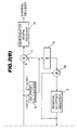
- a signal from the receiver front end (not shown) is filtered in an IF filter 1, amplified in a programmable gain amplifier 2, and applied as one input to a mixer 3 whose other input, supplied by a local oscillator 4, is at a frequency whereby the mixer output is at baseband.
- the mixer output comprises both I and Q components, but for the sake of clarity only one component, and the associated circuitry, will be considered.
- the baseband output may contain a dc offset, the magnitude of which may be dependent on factors such as temperature, and the gain of amplifier 2.
- the baseband output is applied to the positive input of a summing amplifier 5 whose output is fed to an antialiasing filter 6 which in turn feeds an A/D converter 7.
- the output of A/D converter 7 is fed to a demodulator or digital receiver 18. Any dc offset in the baseband signal reduces the useable dynamic range of the A/D converter 7, and degrades the performance of the demodulator 18 and any subsequent channel decoder (not shown).
- Summing amplifier 5 itself may introduce an additional dc offset to the baseband signal.
- the dc offset is estimated regularly, and a signal representative of it is applied to the negative input of summing amplifier 5 so as to compensate for the dc offset prior to the A/D converter 7.
- Estimation of the d.c. offset is usually done during receive gaps as follows.
- the input to the amplifier 2 is grounded so as to shunt any signal from the RF front end to ground.
- a normally open switch 12 is closed, i.e. it is switched to the calibration mode, and a low pass filter 14 filters out the dc offset in the baseband signal.
- the charge acquired on a capacitor in filter 14 is an estimate of the dc offset and is applied to the negative input of amplifier 5 which subtracts the estimate from the baseband signal.
- switch 12 is opened, and normal reception is resumed.
- mixer 3 provides both I and Q output components
- a further summing amplifier 5 filter 6, A/D converter 7, switch 12 and low pass filter 14, none of which is shown, are required to process the other component.
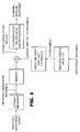
- dc offset compensation is effected as follows.
- An initial dc offset estimate is required because the dc offset in the baseband signal output of mixer 3 may be a significant, or even the major, component of the baseband signal.
- a dc offset of significant magnitude may swamp the A/D converter 7 and cause it to give an erroneous output, with a consequent deleterious effect on subsequent circuit elements.
- Initial dc offset estimation is effected by grounding the input to amplifier 2.
- Switches 12 and 13 are closed, i.e. switched to the calibration mode, and a low pass filter 14 filters out the dc offset in the baseband signal.
- the charge acquired on a capacitor in filter 14 is an estimate of the dc offset and is converted to digital form by an A/D converter 15 and stored in a dc offset register 16.
- the input to amplifier 2 is then ungrounded and switches 12 and 13 are opened, i.e. switched to the normal mode.
- the estimate stored in register 16 is applied via summer 10, of which more later, to a D/A converter 11 which provides an analog version of the stored dc offset estimate to the negative input of summing amplifier 5, which in turn subtracts the dc offset estimate from the baseband signal.
- the output of amplifier 5 is provided, via an antialising filter 6, to an A/D converter 7 whose output feeds a demodulator or digital receiver 18 and channel decoder (not shown). Removal of the dc offset from the baseband signal enables the full dynamic range of the A/D converter 7 to be used, and avoids degrading the performance of the demodulator 18. Because the dc offset estimate is stored in register 16, subsequent charge leakage in the capacitor in filter 14 is of no effect.
- Estimator 8 may be a processor adapted to operate under the control of a suitable algorithm to produce an estimate of the residual dc offset.
- estimator 8 requires both I and Q inputs to perform the exemplary algorithms.
- the estimate stored in register 9 is summed in summer 10 with the estimate stored in register 16, and the sum is converted to analog form in D/A converter 11 whose output is subtracted from the baseband signal in amplifier 5 to provide an output which is substantially free of dc offset.
- a summer 20 is fed with output from register 9 and output from time delay 19 so as to update register 9 as changes in the residual dc offset occur.
- the output of estimator 8 also feeds a subtractor 17 so that changes in the residual dc offset can be subtracted instantaneously from the signal fed to the demodulator 18.
- the delay provided by time delay 19 is chosen so as to prevent the residual dc offset estimate produced by estimator 8 from being subtracted twice over, once in amplifier 5, and again at the output of A/D converter 7.
- estimator 8 is fed with both I and Q input components.
- Figs. 2A and 2B show only the circuit elements for processing one of these components; for processing the other component a further set of components 5 to 7, 9 to 17 and 19 is required.
- the demodulator 18 will always receive a signal substantially free of dc offset, and the useable dynamic range of A/D converter 7 will be maximised.
- switch 12 shown connected to the output of mixer 3, could instead be connected to the output of summing amplifier 5.
- the initial dc offset estimation would then take into account any dc offset introduced by amplifier 5 itself.
- the contents of these registers could be individually subtracted from the baseband signal, e.g. by summing amplifier 5 subtracting only the dc offset estimate, and another subtractor fed with output from amplifier 5 for subtracting the residual dc offset estimate after any necessary D/A conversion.
- FIGS. 2C and 2D Another receiver embodying the invention will now be desribed with reference to FIGS. 2C and 2D in which components bearing the same reference signs as those in FIGS. 2A and 2B perform corresponding functions as already described.
- Offset calculation logic 22 includes a comparator (not shown) which is fed with output from the A/D converter 7 and which provides a signal representative of whether the DC offset in the A/D converter's output is positive. negative, or zero. Offset calculation logic 22 also includes logic circuitry (not shown) which provides to D/A converter 11 an offset compensation signal dependent upon whether the comparator output represents a positive or negative DC offset. The output of D/A converter 11 is subtracted in amplifier 5 from the baseband signal, and the output of A/D converter 7 is again examined by the comparator in offset calculation logic 22 to repeat the process just described.
- the estimate stored in register 9 is summed in summer 10 with the estimate stored in registers 16', and the sum is converted to analog form in D/A converter 11 prior to subtraction from the baseband signal in amplifier 5 to provide an output which is substantially free of DC offset.
- DC offset registers 16' effectively constitute a form of look-up table which provides to summer 10 the DC offset estimate appropriate to the gain setting of amplifier 2 in accordance with a "gain select" signal on lead 24. Storing a plurality of DC offset estimates avoids the need to perform an initial DC offset estimation process each time the gain of amplifier 2 is changed.
Applications Claiming Priority (2)
| Application Number | Priority Date | Filing Date | Title |
|---|---|---|---|
| US9690098A | 1998-06-12 | 1998-06-12 | |
| US96900 | 1998-06-12 |
Publications (1)
| Publication Number | Publication Date |
|---|---|
| EP0964557A1 true EP0964557A1 (de) | 1999-12-15 |
Family
ID=22259633
Family Applications (1)
| Application Number | Title | Priority Date | Filing Date |
|---|---|---|---|
| EP99304097A Withdrawn EP0964557A1 (de) | 1998-06-12 | 1999-05-26 | Empfänger mit Gleichstromoffsetkompensation |
Country Status (1)
| Country | Link |
|---|---|
| EP (1) | EP0964557A1 (de) |
Cited By (18)
| Publication number | Priority date | Publication date | Assignee | Title |
|---|---|---|---|---|
| GB2355900A (en) * | 1999-10-29 | 2001-05-02 | Ericsson Telefon Ab L M | Radio receiver |
| WO2002029968A2 (en) * | 2000-10-02 | 2002-04-11 | Intersil Americas Inc. | Quardrature direct-conversion demodolator using dc offset compensation |
| EP1202445A1 (de) * | 2000-10-30 | 2002-05-02 | Texas Instruments France | Vorrichtung zum Ausgleichen des DC-Offsets eines Quadratur-Demodulators , und Verfahren dazu |
| EP1235355A2 (de) * | 2001-02-26 | 2002-08-28 | STMicroelectronics S.A. | Verfahren und Vorrichtung zur Gleichspannungsschiebungskompensation eines Direktmischempfängers |
| US6735422B1 (en) | 2000-10-02 | 2004-05-11 | Baldwin Keith R | Calibrated DC compensation system for a wireless communication device configured in a zero intermediate frequency architecture |
| EP1503494A1 (de) * | 2003-07-31 | 2005-02-02 | Broadcom Corporation | Quadraturempfänger unter Verwendung von Gleichspannungsoffsetkompensation |
| WO2005101671A2 (en) | 2004-04-13 | 2005-10-27 | Maxlinear, Inc. | Method and apparatus for dc offset removal |
| EP1603228A1 (de) * | 2004-06-04 | 2005-12-07 | Infineon Technologies AG | Vorrichtung zur DC-Kompensation in einem Demodulator |
| US7068987B2 (en) | 2000-10-02 | 2006-06-27 | Conexant, Inc. | Packet acquisition and channel tracking for a wireless communication device configured in a zero intermediate frequency architecture |
| WO2007038782A1 (en) * | 2005-09-28 | 2007-04-05 | Qualcomm Incorporated | Dc offset cancellation circuit for a receiver |
| DE102005054239A1 (de) * | 2005-11-14 | 2007-05-16 | Infineon Technologies Ag | Adaptive DC-Offset-Kompensation in einem Funkempfänger |
| US7412222B2 (en) | 2003-05-20 | 2008-08-12 | Broadcom Corporation | Quadrature correction method for analog television reception using direct-conversion tuners |
| US7536165B2 (en) | 2002-07-24 | 2009-05-19 | Nxp B.V. | Offset correction for down-conversion mixers |
| US8285240B2 (en) | 2004-12-10 | 2012-10-09 | Maxlinear, Inc. | Harmonic reject receiver architecture and mixer |
| US8306157B2 (en) | 2004-10-12 | 2012-11-06 | Maxlinear, Inc. | Receiver architecture with digitally generated intermediate frequency |
| US8311156B2 (en) | 2004-10-12 | 2012-11-13 | Maxlinear, Inc. | Hybrid receiver architecture using upconversion followed by direct downconversion |
| US8396173B2 (en) | 2007-10-01 | 2013-03-12 | Maxlinear, Inc. | I/Q calibration techniques |
| US11509338B2 (en) | 2020-03-18 | 2022-11-22 | Analog Devices, Inc. | Nested feedback for offset cancellation in a wireline receiver |
Citations (5)
| Publication number | Priority date | Publication date | Assignee | Title |
|---|---|---|---|---|
| US5459679A (en) * | 1994-07-18 | 1995-10-17 | Quantum Corporation | Real-time DC offset control and associated method |
| WO1995030275A1 (en) * | 1994-04-28 | 1995-11-09 | Qualcomm Incorporated | Method and apparatus for automatic gain control and dc offset cancellation in quadrature receiver |
| US5663988A (en) * | 1992-01-18 | 1997-09-02 | Alcatel Sel Aktiengesellschaft | Method and circuit arrangement for offset correction in a TDMA radio receiver |
| US5699011A (en) * | 1996-08-02 | 1997-12-16 | Zenith Electronics Corporation | DC offset compensation method and apparatus |
| US5748681A (en) * | 1995-10-27 | 1998-05-05 | Lucent Technologies Inc | Offset correction for a homodyne radio |
-
1999
- 1999-05-26 EP EP99304097A patent/EP0964557A1/de not_active Withdrawn
Patent Citations (5)
| Publication number | Priority date | Publication date | Assignee | Title |
|---|---|---|---|---|
| US5663988A (en) * | 1992-01-18 | 1997-09-02 | Alcatel Sel Aktiengesellschaft | Method and circuit arrangement for offset correction in a TDMA radio receiver |
| WO1995030275A1 (en) * | 1994-04-28 | 1995-11-09 | Qualcomm Incorporated | Method and apparatus for automatic gain control and dc offset cancellation in quadrature receiver |
| US5459679A (en) * | 1994-07-18 | 1995-10-17 | Quantum Corporation | Real-time DC offset control and associated method |
| US5748681A (en) * | 1995-10-27 | 1998-05-05 | Lucent Technologies Inc | Offset correction for a homodyne radio |
| US5699011A (en) * | 1996-08-02 | 1997-12-16 | Zenith Electronics Corporation | DC offset compensation method and apparatus |
Cited By (36)
| Publication number | Priority date | Publication date | Assignee | Title |
|---|---|---|---|---|
| GB2355900B (en) * | 1999-10-29 | 2004-03-17 | Ericsson Telefon Ab L M | Radio receiver |
| GB2355900A (en) * | 1999-10-29 | 2001-05-02 | Ericsson Telefon Ab L M | Radio receiver |
| US6711393B1 (en) | 1999-10-29 | 2004-03-23 | Telefonaktiebolaget Lm Ericsson (Publ) | Radio receiver |
| US6735422B1 (en) | 2000-10-02 | 2004-05-11 | Baldwin Keith R | Calibrated DC compensation system for a wireless communication device configured in a zero intermediate frequency architecture |
| WO2002029968A3 (en) * | 2000-10-02 | 2002-06-13 | Intersil Inc | Quardrature direct-conversion demodolator using dc offset compensation |
| US7068987B2 (en) | 2000-10-02 | 2006-06-27 | Conexant, Inc. | Packet acquisition and channel tracking for a wireless communication device configured in a zero intermediate frequency architecture |
| WO2002029968A2 (en) * | 2000-10-02 | 2002-04-11 | Intersil Americas Inc. | Quardrature direct-conversion demodolator using dc offset compensation |
| USRE42799E1 (en) | 2000-10-02 | 2011-10-04 | Intellectual Ventures I Llc | Packet acquisition and channel tracking for a wireless communication device configured in a zero intermediate frequency architecture |
| EP1202445A1 (de) * | 2000-10-30 | 2002-05-02 | Texas Instruments France | Vorrichtung zum Ausgleichen des DC-Offsets eines Quadratur-Demodulators , und Verfahren dazu |
| EP1235355A2 (de) * | 2001-02-26 | 2002-08-28 | STMicroelectronics S.A. | Verfahren und Vorrichtung zur Gleichspannungsschiebungskompensation eines Direktmischempfängers |
| FR2821500A1 (fr) * | 2001-02-26 | 2002-08-30 | St Microelectronics Sa | Procede et dispositif de compensation du decalage cc dynamique d'un recepteur a conversion directe |
| EP1235355A3 (de) * | 2001-02-26 | 2002-09-18 | STMicroelectronics S.A. | Verfahren und Vorrichtung zur Gleichspannungsschiebungskompensation eines Direktmischempfängers |
| US7536165B2 (en) | 2002-07-24 | 2009-05-19 | Nxp B.V. | Offset correction for down-conversion mixers |
| US8165554B2 (en) | 2003-05-20 | 2012-04-24 | Gomez Ramon A | Quadrature correction method for analog television reception using direct-conversion tuners |
| US7412222B2 (en) | 2003-05-20 | 2008-08-12 | Broadcom Corporation | Quadrature correction method for analog television reception using direct-conversion tuners |
| US7787056B2 (en) | 2003-07-31 | 2010-08-31 | Broadcom Corporation | Apparatus and method for restoring DC spectrum for analog television reception using direct conversion tuners |
| EP1503494A1 (de) * | 2003-07-31 | 2005-02-02 | Broadcom Corporation | Quadraturempfänger unter Verwendung von Gleichspannungsoffsetkompensation |
| US7295250B2 (en) | 2003-07-31 | 2007-11-13 | Broadcom Corporation | Apparatus and method for restoring DC spectrum for analog television reception using direct conversion turners |
| US8718584B2 (en) | 2004-04-13 | 2014-05-06 | Maxlinear, Inc. | Dual conversion receiver with programmable intermediate frequency and channel selection |
| US7532870B2 (en) | 2004-04-13 | 2009-05-12 | Maxlinear, Inc. | Method and apparatus for DC offset removal |
| US7778613B2 (en) | 2004-04-13 | 2010-08-17 | Maxlinear, Inc. | Dual conversion receiver with programmable intermediate frequency and channel selection |
| WO2005101671A3 (en) * | 2004-04-13 | 2006-01-12 | Maxlinear Inc | Method and apparatus for dc offset removal |
| WO2005101671A2 (en) | 2004-04-13 | 2005-10-27 | Maxlinear, Inc. | Method and apparatus for dc offset removal |
| US7436236B2 (en) | 2004-06-04 | 2008-10-14 | Infineon Technologies Ag | Analog DC compensation |
| EP1603228A1 (de) * | 2004-06-04 | 2005-12-07 | Infineon Technologies AG | Vorrichtung zur DC-Kompensation in einem Demodulator |
| CN100380826C (zh) * | 2004-06-04 | 2008-04-09 | 因芬尼昂技术股份公司 | 模拟补偿交流信号中的直流分量的装置 |
| US8306157B2 (en) | 2004-10-12 | 2012-11-06 | Maxlinear, Inc. | Receiver architecture with digitally generated intermediate frequency |
| US8311156B2 (en) | 2004-10-12 | 2012-11-13 | Maxlinear, Inc. | Hybrid receiver architecture using upconversion followed by direct downconversion |
| US8285240B2 (en) | 2004-12-10 | 2012-10-09 | Maxlinear, Inc. | Harmonic reject receiver architecture and mixer |
| WO2007038782A1 (en) * | 2005-09-28 | 2007-04-05 | Qualcomm Incorporated | Dc offset cancellation circuit for a receiver |
| CN101313463B (zh) * | 2005-09-28 | 2013-03-27 | 高通股份有限公司 | 用于接收机的dc偏移消除电路 |
| US8036622B2 (en) | 2005-09-28 | 2011-10-11 | Qualcomm, Incorporated | DC offset cancellation circuit for a receiver |
| DE102005054239A1 (de) * | 2005-11-14 | 2007-05-16 | Infineon Technologies Ag | Adaptive DC-Offset-Kompensation in einem Funkempfänger |
| US8396173B2 (en) | 2007-10-01 | 2013-03-12 | Maxlinear, Inc. | I/Q calibration techniques |
| US9680674B2 (en) | 2007-10-01 | 2017-06-13 | Maxlinear, Inc. | I/Q calibration techniques |
| US11509338B2 (en) | 2020-03-18 | 2022-11-22 | Analog Devices, Inc. | Nested feedback for offset cancellation in a wireline receiver |
Similar Documents
| Publication | Publication Date | Title |
|---|---|---|
| EP0964557A1 (de) | Empfänger mit Gleichstromoffsetkompensation | |
| EP0948128B1 (de) | Unterdrückung von Gleichspannungsverschiebungen in einem Quadraturempfänger | |
| EP2232714B1 (de) | System und verfahren zur korrektur von intermodulation zweiter ordnung für einen empfänger | |
| JP4072061B2 (ja) | 無線受信機用dcオフセット補正方式 | |
| CN101895266B (zh) | 数模混合自动增益控制系统及其控制方法 | |
| US6985711B2 (en) | Direct current offset cancellation for mobile station modems using direct conversion | |
| EP0757858B1 (de) | Verfahren und vorrichtung zur automatischen verstärkungsregelung in einem digitalen empfänger | |
| US6757340B1 (en) | Radio receiver and method for preloading an average DC-offset into a channel filter | |
| KR100864558B1 (ko) | 왜곡 보상 장치 및 왜곡 보상 방법 | |
| JPH08242262A (ja) | Dcオフセット補正回路 | |
| US7583765B2 (en) | DC offset detection and cancellation in a receiver | |
| WO2003096526A1 (fr) | Procede de correction de distorsion hybride et dispositif de correction de distorsion hybride | |
| US7336937B2 (en) | Compensation of a DC offset in a receiver | |
| EP1172928A2 (de) | Offsetgleichspannungskorrektur und AGC für Null-ZF-Funkempfänger | |
| CN104811404A (zh) | 直流偏移校正方法和装置 | |
| US6882208B1 (en) | Adjustment of amplitude and DC offsets in a digital receiver | |
| US6445736B1 (en) | GSM baseband receiver arrangement using digital signal processing | |
| JP3576410B2 (ja) | 受信装置と送受信装置及び方法 | |
| JPH1013482A (ja) | Dcオフセット除去機能を備えた受信機及びこれを用いた無線通信システム | |
| CN100449937C (zh) | 信号处理方法及信号处理设备 | |
| KR20050061393A (ko) | 주파수 직접 변환 장치에서 직류 옵셋 제거 장치 및 방법 | |
| EP1499014A1 (de) | Verfahren zur automatischen Verstärkungsregelung, beispielsweise in einem Telekommunikationssystem, Vorrichtung und Computerprogramm hierfür | |
| CN116996348A (zh) | 毛刺回避处理方法、装置、设备及可读存储介质 | |
| WO2014091270A1 (en) | Method and device for estimation and correction of i/q mismatch using iterative loops | |
| KR20100057434A (ko) | 수신기에서의 이미지 제거 장치 |
Legal Events
| Date | Code | Title | Description |
|---|---|---|---|
| PUAI | Public reference made under article 153(3) epc to a published international application that has entered the european phase |
Free format text: ORIGINAL CODE: 0009012 |
|
| AK | Designated contracting states |
Kind code of ref document: A1 Designated state(s): DE |
|
| AX | Request for extension of the european patent |
Free format text: AL;LT;LV;MK;RO;SI |
|
| 17P | Request for examination filed |
Effective date: 20000602 |
|
| AKX | Designation fees paid |
Free format text: DE |
|
| STAA | Information on the status of an ep patent application or granted ep patent |
Free format text: STATUS: THE APPLICATION IS DEEMED TO BE WITHDRAWN |
|
| 18D | Application deemed to be withdrawn |
Effective date: 20021203 |