EP0964504A1 - Schaltnetzteil - Google Patents
Schaltnetzteil Download PDFInfo
- Publication number
- EP0964504A1 EP0964504A1 EP99118477A EP99118477A EP0964504A1 EP 0964504 A1 EP0964504 A1 EP 0964504A1 EP 99118477 A EP99118477 A EP 99118477A EP 99118477 A EP99118477 A EP 99118477A EP 0964504 A1 EP0964504 A1 EP 0964504A1
- Authority
- EP
- European Patent Office
- Prior art keywords
- power source
- circuit
- switch element
- current
- primary winding
- Prior art date
- Legal status (The legal status is an assumption and is not a legal conclusion. Google has not performed a legal analysis and makes no representation as to the accuracy of the status listed.)
- Granted
Links
Images


Classifications
-
- H—ELECTRICITY
- H02—GENERATION; CONVERSION OR DISTRIBUTION OF ELECTRIC POWER
- H02M—APPARATUS FOR CONVERSION BETWEEN AC AND AC, BETWEEN AC AND DC, OR BETWEEN DC AND DC, AND FOR USE WITH MAINS OR SIMILAR POWER SUPPLY SYSTEMS; CONVERSION OF DC OR AC INPUT POWER INTO SURGE OUTPUT POWER; CONTROL OR REGULATION THEREOF
- H02M1/00—Details of apparatus for conversion
- H02M1/42—Circuits or arrangements for compensating for or adjusting power factor in converters or inverters
- H02M1/4208—Arrangements for improving power factor of AC input
- H02M1/4258—Arrangements for improving power factor of AC input using a single converter stage both for correction of AC input power factor and generation of a regulated and galvanically isolated DC output voltage
-
- Y—GENERAL TAGGING OF NEW TECHNOLOGICAL DEVELOPMENTS; GENERAL TAGGING OF CROSS-SECTIONAL TECHNOLOGIES SPANNING OVER SEVERAL SECTIONS OF THE IPC; TECHNICAL SUBJECTS COVERED BY FORMER USPC CROSS-REFERENCE ART COLLECTIONS [XRACs] AND DIGESTS
- Y02—TECHNOLOGIES OR APPLICATIONS FOR MITIGATION OR ADAPTATION AGAINST CLIMATE CHANGE
- Y02B—CLIMATE CHANGE MITIGATION TECHNOLOGIES RELATED TO BUILDINGS, e.g. HOUSING, HOUSE APPLIANCES OR RELATED END-USER APPLICATIONS
- Y02B70/00—Technologies for an efficient end-user side electric power management and consumption
- Y02B70/10—Technologies improving the efficiency by using switched-mode power supplies [SMPS], i.e. efficient power electronics conversion e.g. power factor correction or reduction of losses in power supplies or efficient standby modes
Definitions
- the present invention relates to a switching power source apparatus which receives alternating current such as commercial alternating-current power source as input.
- the switching power source apparatus is widely used recently as a power source circuit for various electronic appliances owing to its efficient power transforming characteristic. In most of such circuits, however, since the input rectifying circuit of capacitor input type is used, the power factor is poor, and harmonic currents contained in the input current may cause troubles in other electronic appliances.
- Fig. 5 shows a circuit construction of a conventional switching power source apparatus.
- reference numeral 1 denotes an input alternating-current power source
- 2 is an input filter capacitor, which is connected to both ends of the input alternating-current power source 1.
- Reference numeral 3 denotes a full-wave rectifying circuit, which is composed of diodes 31 to 34.
- Reference numeral 4 is a smoothing capacitor, and an input rectifying circuit of capacitor input type which rectifies and smoothes the alternating-current input voltage of the input alternating-current power source 1 is constituted with the full-wave rectifying circuit 3 and smoothing capacitor 4.
- Reference numeral 8 represents a transformer, which possesses a primary winding 81 and a secondary winding 82.
- Reference numeral 9 is a switch element, and a series circuit of the primary winding 81 and switch element 9 is connected to both ends of the smoothing capacitor 4.
- Reference numeral 20 is a rectifying and smoothing circuit, composed of diodes 21, 22, a choke coil 23, and a capacitor 24, which rectifies and smoothes the voltage generated in the secondary winding 82 by on/off action of the switch element 9, and supplies an output direct-current voltage to a load 25.
- Reference numeral 40 is a control circuit, which controls the on/off ratio of the switch element 9 so as to stabilize the output direct-current voltage supplied to the load 25.
- an input waveform is shown in Fig. 6.
- the full-wave rectifying circuit 3 conducts at only near its peak value, and the charging current to the smoothing capacitor 4 is concentrated, so that the input current waveform has a peak form short in the conduction period.
- Fig. 7 the parts having the same actions as in Fig. 5 are identified with same reference numerals.
- reference numeral 1 is an input alternating-current power source
- 2 is an input filter capacitor, which is connected to both ends of the input alternating-current power source 1.
- Reference numeral 3 denotes a full-wave rectifying circuit, composed of diodes 31 to 34.
- Reference numeral 4 is a smoothing capacitor
- 5 is a choke coil, and one end of the choke coil 5 is connected to the positive electrode output end of the full-wave rectifying circuit 3.
- Reference numeral 8 represents a transformer, which comprises a primary winding 81, a secondary winding 82, a tertiary winding 83 connected to the other end of the choke coil 5, and a quaternary winding 84.
- a reference numeral 9 is a switch element, and a series circuit of the primary winding 81 and the switch element 9 is connected to both ends of the smoothing capacitor 4.
- Reference numeral 19 is a diode, and its series circuit with the quaternary winding 84 is connected to both ends of the smoothing capacitor 4.
- Reference numeral 20 is a rectifying and smoothing circuit, composed of diodes 21, 22, a choke coil 23, and a capacitor 24, which rectifies and smoothes the voltage generated in the secondary winding 82 by on/off action of the switch element 9, and supplies an output direct-current voltage to a load 25.
- Reference numeral 40 denotes a control circuit, which controls the on/off ratio of the switch element 9 so as to stabilize the output direct-current voltage supplied to the load 25.
- the diode 32 acts instead of the diode 31, and the diode 34, instead of the diode 33.
- (a) denotes an output voltage waveform of the full-wave rectifying circuit 3
- (b) is a current waveform flowing in the choke coil 5
- (c) is an input current waveform.
- the current flowing in the choke coil 5 is a sawtooth waveform having a peak value proportional to the voltage of the input alternating-current power source 1. It is smoothed by the filter capacitor 2 to produce an input current waveform, which is a sinusoidal waveform approximately proportional to the input alternating-current voltage.
- the full-wave rectifying circuit 3 does not conduct when Vi-(1-N)Ec ⁇ 0 , and the input current waveform becomes as shown by broken line in the diagram.
- the switching power source apparatus of the invention comprises the features of claims 1 and 3, respectively. Preferred embodiments thereof are subject matter of the dependent claims.
- reference numeral 1 denotes an input alternating-current power source
- 2 is a filter capacitor, which is connected to both ends of the input alternating-current power source.
- Reference numeral 3 is a full-wave rectifying circuit, composed of diodes 31 to 34, which rectifies the input alternating-current voltage of the input alternating-current power source 1.
- Reference numeral 4 is a smoothing capacitor, which is connected to the output end of the full-wave rectifying circuit 3.
- Reference numeral 61 is a first diode, 62 is a second diode, and the anode terminals of the first diode 61 and second diode 62 are connected to the input alternating-current power source 1, and the cathode terminals are connected with each other.
- Reference numeral 8 represents a transformer, which possesses a primary winding 81 and a secondary winding 82.
- Reference numeral 9 denotes a switch element, and a series circuit of the primary winding 81 and switch element 9 is connected to both ends of the smoothing capacitor 4.
- the connection point of the primary winding 81 and switch element 9, and the cathode terminals of the first diode 61 and second diode 62 are connected with each other.
- Reference numeral 20 is a rectifying and smoothing circuit, which is composed of diodes 21, 22, a choke coil 23, and a capacitor 24.
- the rectifying and smoothing circuit 20 is connected to the secondary winding 82, and rectifies and smoothes the voltage generated in the secondary winding 82 by on/off action of the switch element 9.
- Reference numeral 25 represents a load, which is connected to the output end of the rectifying and smoothing circuit 20, and a direct-current output voltage is supplied.
- Reference numeral 40 is a control circuit, which controls the on/off ratio of the switch element 9 so as to stabilize the direct-current output voltage supplied to the load 25.
- the portion composed of the smoothing capacitor 4, transformer 8, switch element 9, rectifying and smoothing circuit 20, load 25 and control circuit 40 operates same as an ordinary DC/DC converter, and hence the explanation is omitted.
- first and second choke coils 51, 52 is connected to the both ends of the input alternating-current power source 1.
- the anode terminals of the first diode 61 and diode 31 are connected, and at the other end of the second choke coil 52, the anode terminals of the second diode 62 and diode 32 are connected.
- the cathode terminals of the first and second diodes are connected to the connection point of the primary winding 81 and switch element 9.
- the cathode terminals of the diode 31 and diode 32 are connected to the connection point of the smoothing capacitor 4 and primary winding 81.
- the cathode terminals of the diodes 33, 34 are connected to both ends of the input alternating-current power source 1, and the anode terminals are connected to the connection point of the switch element 9 and smoothing capacitor 4.
- the diode 31 conducts instead of the diode 61, and the current flows in the route of input alternating-current power source 1 ⁇ first choke coil 51 ⁇ diode 31 ⁇ smoothing capacitor 4 ⁇ diode 33 ⁇ input alternating-current power source 1.
- first choke coil 51 the difference of the voltages of the input alternating-current power source 1 and smoothing capacitor 4 is applied, and this current decreases linearly, and soon becomes zero.
- the second choke coil 52 operates instead of the first choke coil 51, the diode 62, instead of the diode 61, the diode 32 instead of the diode 31, and the diode 34, instead of the diode 33.
- the current flowing in the first and second choke coils 51, 52 becomes a sawtooth waveform possessing a peak value proportional to the voltage of the input alternating-current power source 1. It is smoothed by the filter capacitor to obtain an input current waveform, which is a sinusoidal waveform approximately proportional to the input alternating-current voltage.
- the input waveform is improved, and enhancement of power factor and reduction of harmonic current currents are realized, and as compared with the switching power source apparatus shown in Fig. 6, the current of the first and second choke coils 51 and 52 flows without passing through the transformer 8, so that the conduction loss can be reduced.
- Fig. 2 is a circuit constitutional diagram showing the sixth embodiment of the invention.
- the transformer 8 further comprises a tertiary winding 83 having one end connected to one end of the primary winding 81, and that the cathode terminals of the first and second diodes 61, 62 are connected to the other end of the tertiary winding 83.
- the diode 31 conducts instead of the diode 61, and the current flows in the route of input alternating-current power source 1 ⁇ first choke coil 51 ⁇ diode 31 ⁇ smoothing capacitor 4 ⁇ diode 33 ⁇ input alternating-current power source.
- Vi-Ec Vi-Ec is applied, and this current decreases linearly, and soon becomes zero.
- the second choke coil 52 operates instead of the choke coil 51, the diode 62, instead of the diode 61, the diode 32, instead of the diode 31, and the diode 34, instead of the diode 33.
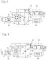
- Fig. 3 is a circuit constitutional diagram showing the third embodiment of the invention.
- first and second diodes 61, 62 are replaced by first and second capacitors 71, 72.
- the second choke coil 52 operates instead of the first choke coil 51, the diode 62, instead of the diode 61, the diode 32, instead of the diode 31, and the diode 34, instead of the diode 33.
- Fig. 4 is a circuit constitutional diagram showing the fourth embodiment of the invention.
- the first and second diodes 61, 62 are replaced by first and second capacitors 71, 72.
- a series circuit of diode 10 and quaternary winding 84 is provided at both ends of the smoothing capacitor 4, and the magnetic reset of the transformer 4 can be done efficiently.
- the effect of the presence or absence of the series circuit of the diode 10 and quaternary winding 84 on the operation of the invention is not relatively large on the effect of the invention, and it not indispensable for explanation of the invention, and hence it was omitted in the foregoing embodiments.
Landscapes
- Engineering & Computer Science (AREA)
- Power Engineering (AREA)
- Dc-Dc Converters (AREA)
- Rectifiers (AREA)
Applications Claiming Priority (7)
| Application Number | Priority Date | Filing Date | Title |
|---|---|---|---|
| JP800994 | 1994-01-28 | ||
| JP800994 | 1994-01-28 | ||
| JP1303994 | 1994-02-07 | ||
| JP1304094 | 1994-02-07 | ||
| JP1304094 | 1994-02-07 | ||
| JP1303994 | 1994-02-07 | ||
| EP95100975A EP0665632B1 (de) | 1994-01-28 | 1995-01-25 | Schalt-Stromversorgungsgerät |
Related Parent Applications (1)
| Application Number | Title | Priority Date | Filing Date |
|---|---|---|---|
| EP95100975A Division EP0665632B1 (de) | 1994-01-28 | 1995-01-25 | Schalt-Stromversorgungsgerät |
Publications (2)
| Publication Number | Publication Date |
|---|---|
| EP0964504A1 true EP0964504A1 (de) | 1999-12-15 |
| EP0964504B1 EP0964504B1 (de) | 2004-05-06 |
Family
ID=27277839
Family Applications (3)
| Application Number | Title | Priority Date | Filing Date |
|---|---|---|---|
| EP97110563A Expired - Lifetime EP0802615B1 (de) | 1994-01-28 | 1995-01-25 | Schaltnetzteil |
| EP99118477A Expired - Lifetime EP0964504B1 (de) | 1994-01-28 | 1995-01-25 | Schaltnetzteil |
| EP95100975A Expired - Lifetime EP0665632B1 (de) | 1994-01-28 | 1995-01-25 | Schalt-Stromversorgungsgerät |
Family Applications Before (1)
| Application Number | Title | Priority Date | Filing Date |
|---|---|---|---|
| EP97110563A Expired - Lifetime EP0802615B1 (de) | 1994-01-28 | 1995-01-25 | Schaltnetzteil |
Family Applications After (1)
| Application Number | Title | Priority Date | Filing Date |
|---|---|---|---|
| EP95100975A Expired - Lifetime EP0665632B1 (de) | 1994-01-28 | 1995-01-25 | Schalt-Stromversorgungsgerät |
Country Status (2)
| Country | Link |
|---|---|
| EP (3) | EP0802615B1 (de) |
| DE (3) | DE69531868T8 (de) |
Families Citing this family (7)
| Publication number | Priority date | Publication date | Assignee | Title |
|---|---|---|---|---|
| EP0844728B1 (de) * | 1996-11-25 | 2002-04-10 | Samsung Electronics Co., Ltd. | Durchflussumrichter |
| CN1074604C (zh) * | 1998-08-20 | 2001-11-07 | 深圳市安圣电气有限公司 | 零开关损耗开关电源 |
| JP2001095247A (ja) * | 1999-09-21 | 2001-04-06 | Sony Corp | スイッチング電源回路 |
| JP3496717B2 (ja) * | 2001-04-18 | 2004-02-16 | サンケン電気株式会社 | スイッチング電源装置 |
| DE10144540A1 (de) | 2001-09-11 | 2003-04-03 | Infineon Technologies Ag | Spannungswandler |
| CN113405446B (zh) * | 2021-05-11 | 2023-08-08 | 联合汽车电子有限公司 | 一种检测变压器磁芯间隙的方法及装置 |
| CN113741605B (zh) * | 2021-08-05 | 2023-05-09 | 大族激光科技产业集团股份有限公司 | 一种线性稳压电源 |
Citations (3)
| Publication number | Priority date | Publication date | Assignee | Title |
|---|---|---|---|---|
| JPS56150972A (en) * | 1980-04-25 | 1981-11-21 | Hitachi Ltd | Power circuit |
| DE4131240A1 (de) * | 1990-09-19 | 1992-03-26 | Hitachi Ltd | Stromversorgungseinrichtung |
| GB2261331A (en) * | 1991-10-01 | 1993-05-12 | Origin Electric | High power factor AC/DC convertor |
Family Cites Families (2)
| Publication number | Priority date | Publication date | Assignee | Title |
|---|---|---|---|---|
| JPS58141680A (ja) * | 1982-02-17 | 1983-08-23 | Matsushita Electric Ind Co Ltd | スイツチング式直流安定化電源装置 |
| DE4025322A1 (de) * | 1990-08-10 | 1992-02-13 | Thomson Brandt Gmbh | Netzbetriebene phasenanschnitt-steuerschaltung |
-
1995
- 1995-01-25 EP EP97110563A patent/EP0802615B1/de not_active Expired - Lifetime
- 1995-01-25 DE DE69531868T patent/DE69531868T8/de active Active
- 1995-01-25 DE DE69533003T patent/DE69533003T2/de not_active Expired - Lifetime
- 1995-01-25 EP EP99118477A patent/EP0964504B1/de not_active Expired - Lifetime
- 1995-01-25 DE DE69530878T patent/DE69530878T2/de not_active Expired - Lifetime
- 1995-01-25 EP EP95100975A patent/EP0665632B1/de not_active Expired - Lifetime
Patent Citations (3)
| Publication number | Priority date | Publication date | Assignee | Title |
|---|---|---|---|---|
| JPS56150972A (en) * | 1980-04-25 | 1981-11-21 | Hitachi Ltd | Power circuit |
| DE4131240A1 (de) * | 1990-09-19 | 1992-03-26 | Hitachi Ltd | Stromversorgungseinrichtung |
| GB2261331A (en) * | 1991-10-01 | 1993-05-12 | Origin Electric | High power factor AC/DC convertor |
Non-Patent Citations (1)
| Title |
|---|
| PATENT ABSTRACTS OF JAPAN vol. 006, no. 032 (E - 096) 26 February 1982 (1982-02-26) * |
Also Published As
| Publication number | Publication date |
|---|---|
| EP0665632B1 (de) | 2003-05-28 |
| DE69530878D1 (de) | 2003-07-03 |
| DE69531868T2 (de) | 2004-05-06 |
| DE69531868T8 (de) | 2004-10-14 |
| EP0802615B1 (de) | 2003-10-01 |
| EP0802615A2 (de) | 1997-10-22 |
| EP0964504B1 (de) | 2004-05-06 |
| EP0665632A3 (de) | 1995-09-20 |
| DE69533003D1 (de) | 2004-06-09 |
| EP0665632A2 (de) | 1995-08-02 |
| DE69531868D1 (de) | 2003-11-06 |
| DE69533003T2 (de) | 2004-09-02 |
| EP0802615A3 (de) | 1997-11-05 |
| DE69530878T2 (de) | 2003-12-24 |
Similar Documents
| Publication | Publication Date | Title |
|---|---|---|
| JP3260024B2 (ja) | 電源回路 | |
| US7719139B2 (en) | Power supply unit | |
| US20020012259A1 (en) | Switching power supply having an improved power factor by voltage feedback | |
| KR20030052989A (ko) | 스위칭 전원장치 | |
| US7158389B2 (en) | Switching power supply circuit | |
| EP0964504B1 (de) | Schaltnetzteil | |
| US6396724B1 (en) | Charge-pumped DC bias supply | |
| EP1459432B1 (de) | Spannungswandler für eine stromversorgung | |
| JP3159261B2 (ja) | スナバ回路並びにそれを用いたスイッチング電源装置 | |
| JP3100526B2 (ja) | スイッチング電源装置 | |
| JP3400132B2 (ja) | スイッチング電源 | |
| JP2984519B2 (ja) | スイッチング電源 | |
| JP3238266B2 (ja) | スイッチング電源装置 | |
| JP3102985B2 (ja) | スイッチング電源装置 | |
| JPH07194123A (ja) | 電源装置 | |
| JP4329451B2 (ja) | スイッチング電源装置 | |
| JP3498870B2 (ja) | 交流直流変換電源回路 | |
| JP2021044912A (ja) | 電源回路 | |
| JPH0710170B2 (ja) | 直列共振コンバ−タ | |
| JP3081417B2 (ja) | スイッチング電源 | |
| JPH09224375A (ja) | プッシュプル型スイッチング電源装置 | |
| JPH06205582A (ja) | スイッチング電源 | |
| JPH09103076A (ja) | 直流電源装置 | |
| JPH08182332A (ja) | スイッチング電源 | |
| JPH0787729A (ja) | 電源装置 |
Legal Events
| Date | Code | Title | Description |
|---|---|---|---|
| PUAI | Public reference made under article 153(3) epc to a published international application that has entered the european phase |
Free format text: ORIGINAL CODE: 0009012 |
|
| 17P | Request for examination filed |
Effective date: 19990917 |
|
| AC | Divisional application: reference to earlier application |
Ref document number: 665632 Country of ref document: EP |
|
| AK | Designated contracting states |
Kind code of ref document: A1 Designated state(s): DE FR GB |
|
| RIN1 | Information on inventor provided before grant (corrected) |
Inventor name: SEKINE, YUTAKA Inventor name: YOSHINORI, KOBAYASHI Inventor name: HARUO, WATANABE Inventor name: TAKUYA, ISHI |
|
| RIN1 | Information on inventor provided before grant (corrected) |
Inventor name: SEKINE, YUTAKA Inventor name: YOSHINORI, KOBAYASHI Inventor name: HARUO, WATANABE Inventor name: TAKUYA, ISHI |
|
| RAP1 | Party data changed (applicant data changed or rights of an application transferred) |
Owner name: SHINDENGEN ELECTRIC MANUFACTURING COMPANY, LIMITE Owner name: MATSUSHITA ELECTRIC INDUSTRIAL CO., LTD. |
|
| AKX | Designation fees paid |
Free format text: DE FR GB |
|
| GRAP | Despatch of communication of intention to grant a patent |
Free format text: ORIGINAL CODE: EPIDOSNIGR1 |
|
| RIN1 | Information on inventor provided before grant (corrected) |
Inventor name: SEKINE, YUTAKA Inventor name: YOSHINORI, KOBAYASHI Inventor name: HARUO, WATANABE Inventor name: TAKUYA, ISHI |
|
| RIN1 | Information on inventor provided before grant (corrected) |
Inventor name: SEKINE, YUTAKA Inventor name: YOSHINORI, KOBAYASHI Inventor name: HARUO, WATANABE Inventor name: TAKUYA, ISHI |
|
| GRAS | Grant fee paid |
Free format text: ORIGINAL CODE: EPIDOSNIGR3 |
|
| GRAA | (expected) grant |
Free format text: ORIGINAL CODE: 0009210 |
|
| AC | Divisional application: reference to earlier application |
Ref document number: 0665632 Country of ref document: EP Kind code of ref document: P |
|
| AK | Designated contracting states |
Kind code of ref document: B1 Designated state(s): DE FR GB |
|
| REG | Reference to a national code |
Ref country code: GB Ref legal event code: FG4D |
|
| REF | Corresponds to: |
Ref document number: 69533003 Country of ref document: DE Date of ref document: 20040609 Kind code of ref document: P |
|
| ET | Fr: translation filed | ||
| PLBE | No opposition filed within time limit |
Free format text: ORIGINAL CODE: 0009261 |
|
| STAA | Information on the status of an ep patent application or granted ep patent |
Free format text: STATUS: NO OPPOSITION FILED WITHIN TIME LIMIT |
|
| 26N | No opposition filed |
Effective date: 20050208 |
|
| REG | Reference to a national code |
Ref country code: GB Ref legal event code: 732E Free format text: REGISTERED BETWEEN 20110120 AND 20110126 |
|
| REG | Reference to a national code |
Ref country code: FR Ref legal event code: TP Ref country code: FR Ref legal event code: CD |
|
| REG | Reference to a national code |
Ref country code: DE Ref legal event code: R081 Ref document number: 69533003 Country of ref document: DE Owner name: PANASONIC CORPORATION, KADOMA-SHI, JP Free format text: FORMER OWNERS: PANASONIC CORPORATION, KADOMA-SHI, OSAKA, JP; SHINDENGEN ELECTRIC MFG. CO., LTD., HANNO, SAITAMA, JP Effective date: 20110329 Ref country code: DE Ref legal event code: R081 Ref document number: 69533003 Country of ref document: DE Owner name: PANASONIC CORPORATION, KADOMA-SHI, JP Free format text: FORMER OWNER: PANASONIC CORPORATION, SHINDENGEN ELECTRIC MFG. CO., L, , JP Effective date: 20110329 |
|
| PGFP | Annual fee paid to national office [announced via postgrant information from national office to epo] |
Ref country code: GB Payment date: 20130123 Year of fee payment: 19 Ref country code: FR Payment date: 20130204 Year of fee payment: 19 Ref country code: DE Payment date: 20130123 Year of fee payment: 19 |
|
| REG | Reference to a national code |
Ref country code: DE Ref legal event code: R119 Ref document number: 69533003 Country of ref document: DE |
|
| GBPC | Gb: european patent ceased through non-payment of renewal fee |
Effective date: 20140125 |
|
| REG | Reference to a national code |
Ref country code: DE Ref legal event code: R119 Ref document number: 69533003 Country of ref document: DE Effective date: 20140801 |
|
| PG25 | Lapsed in a contracting state [announced via postgrant information from national office to epo] |
Ref country code: DE Free format text: LAPSE BECAUSE OF NON-PAYMENT OF DUE FEES Effective date: 20140801 |
|
| REG | Reference to a national code |
Ref country code: FR Ref legal event code: ST Effective date: 20140930 |
|
| PG25 | Lapsed in a contracting state [announced via postgrant information from national office to epo] |
Ref country code: FR Free format text: LAPSE BECAUSE OF NON-PAYMENT OF DUE FEES Effective date: 20140131 Ref country code: GB Free format text: LAPSE BECAUSE OF NON-PAYMENT OF DUE FEES Effective date: 20140125 |