US7158389B2 - Switching power supply circuit - Google Patents
Switching power supply circuit Download PDFInfo
- Publication number
- US7158389B2 US7158389B2 US10/534,609 US53460903A US7158389B2 US 7158389 B2 US7158389 B2 US 7158389B2 US 53460903 A US53460903 A US 53460903A US 7158389 B2 US7158389 B2 US 7158389B2
- Authority
- US
- United States
- Prior art keywords
- switching
- voltage
- power supply
- current
- circuit
- Prior art date
- Legal status (The legal status is an assumption and is not a legal conclusion. Google has not performed a legal analysis and makes no representation as to the accuracy of the status listed.)
- Expired - Fee Related
Links
Images


Classifications
-
- H—ELECTRICITY
- H02—GENERATION; CONVERSION OR DISTRIBUTION OF ELECTRIC POWER
- H02M—APPARATUS FOR CONVERSION BETWEEN AC AND AC, BETWEEN AC AND DC, OR BETWEEN DC AND DC, AND FOR USE WITH MAINS OR SIMILAR POWER SUPPLY SYSTEMS; CONVERSION OF DC OR AC INPUT POWER INTO SURGE OUTPUT POWER; CONTROL OR REGULATION THEREOF
- H02M1/00—Details of apparatus for conversion
- H02M1/42—Circuits or arrangements for compensating for or adjusting power factor in converters or inverters
- H02M1/4208—Arrangements for improving power factor of AC input
- H02M1/4258—Arrangements for improving power factor of AC input using a single converter stage both for correction of AC input power factor and generation of a regulated and galvanically isolated DC output voltage
-
- H—ELECTRICITY
- H02—GENERATION; CONVERSION OR DISTRIBUTION OF ELECTRIC POWER
- H02M—APPARATUS FOR CONVERSION BETWEEN AC AND AC, BETWEEN AC AND DC, OR BETWEEN DC AND DC, AND FOR USE WITH MAINS OR SIMILAR POWER SUPPLY SYSTEMS; CONVERSION OF DC OR AC INPUT POWER INTO SURGE OUTPUT POWER; CONTROL OR REGULATION THEREOF
- H02M3/00—Conversion of dc power input into dc power output
- H02M3/22—Conversion of dc power input into dc power output with intermediate conversion into ac
- H02M3/24—Conversion of dc power input into dc power output with intermediate conversion into ac by static converters
- H02M3/28—Conversion of dc power input into dc power output with intermediate conversion into ac by static converters using discharge tubes with control electrode or semiconductor devices with control electrode to produce the intermediate ac
-
- H—ELECTRICITY
- H02—GENERATION; CONVERSION OR DISTRIBUTION OF ELECTRIC POWER
- H02M—APPARATUS FOR CONVERSION BETWEEN AC AND AC, BETWEEN AC AND DC, OR BETWEEN DC AND DC, AND FOR USE WITH MAINS OR SIMILAR POWER SUPPLY SYSTEMS; CONVERSION OF DC OR AC INPUT POWER INTO SURGE OUTPUT POWER; CONTROL OR REGULATION THEREOF
- H02M7/00—Conversion of ac power input into dc power output; Conversion of dc power input into ac power output
- H02M7/02—Conversion of ac power input into dc power output without possibility of reversal
- H02M7/04—Conversion of ac power input into dc power output without possibility of reversal by static converters
- H02M7/12—Conversion of ac power input into dc power output without possibility of reversal by static converters using discharge tubes with control electrode or semiconductor devices with control electrode
-
- Y—GENERAL TAGGING OF NEW TECHNOLOGICAL DEVELOPMENTS; GENERAL TAGGING OF CROSS-SECTIONAL TECHNOLOGIES SPANNING OVER SEVERAL SECTIONS OF THE IPC; TECHNICAL SUBJECTS COVERED BY FORMER USPC CROSS-REFERENCE ART COLLECTIONS [XRACs] AND DIGESTS
- Y02—TECHNOLOGIES OR APPLICATIONS FOR MITIGATION OR ADAPTATION AGAINST CLIMATE CHANGE
- Y02B—CLIMATE CHANGE MITIGATION TECHNOLOGIES RELATED TO BUILDINGS, e.g. HOUSING, HOUSE APPLIANCES OR RELATED END-USER APPLICATIONS
- Y02B70/00—Technologies for an efficient end-user side electric power management and consumption
- Y02B70/10—Technologies improving the efficiency by using switched-mode power supplies [SMPS], i.e. efficient power electronics conversion e.g. power factor correction or reduction of losses in power supplies or efficient standby modes
Definitions
- the present invention relates to a switching power supply circuit having a circuit for power factor improvement.
- Switching power supply circuits have a transformer and other devices miniaturized by raising switching frequency, and are used as a power supply for various electronic devices as a high-power DC—DC converter.
- switching power supply circuits having a configuration for power factor improvement added thereto are proposed.
- a switching power supply circuit using a so-called choke input system in which a power choke coil is inserted in series with a commercial alternating-current power supply line to thereby increase a conduction angle of alternating input current and thus improve a power factor (see Japanese Patent Laid-Open No. Hei 7-263262 (FIG. 19)).
- FIG. 27 shows an example of a switching power supply circuit configured to improve a power factor by a choke input system as described above.
- a power factor improving configuration of the choke input system is added to a configuration of a complex resonant converter previously proposed by the present applicant.
- the power supply circuit shown in this figure has a common mode noise filter formed by connecting a common mode choke coil CMC and two across capacitors CL to a commercial alternating-current power supply AC.
- the common mode noise filter suppresses noise transmitted from a switching converter side to the commercial alternating-current power supply AC, for example.
- a rectifying and smoothing circuit comprising a bridge rectifier circuit Di and a smoothing capacitor Ci is provided for a line of the commercial alternating-current power supply AC as shown in the figure.
- This rectifying and smoothing circuit is supplied with the commercial alternating-current power supply AC and then performs a rectifying and smoothing operation, whereby a rectified and smoothed voltage Ei having a level corresponding to the alternating input voltage VAC multiplied by unity is obtained across the smoothing capacitor Ci.
- the rectified and smoothed voltage Ei is supplied as direct-current input voltage to a switching converter in a succeeding stage.
- a power choke coil PCH is inserted in series with the line of the commercial alternating-current power supply AC.
- the power choke coil PCH is inserted in a negative electrode line of the commercial alternating-current power supply AC.
- an inductance Lpch of the power choke coil PCH acts to suppress harmonics of an alternating input current flowing into rectifier diodes forming the bridge rectifier circuit Di from the commercial alternating-current power supply AC. That is, a conduction angle of the alternating input current IAC is increased to improve the power factor.
- the power supply circuit shown in this figure has a complex resonant converter as switching converter that is supplied with the above-mentioned rectified and smoothed voltage Ei for operation.
- the complex resonant converter in this case refers to a switching converter having a resonant circuit added to a primary side or a secondary side thereof in addition to a resonant circuit provided to convert operation of the switching converter into a resonant type operation, so that the plurality of resonant circuits are operated in a complex manner within one switching converter.
- the resonant converter provided as the complex resonant converter in the power supply circuit shown in FIG. 27 is of a current resonant type.
- the current resonant converter in this case has two switching devices Q 1 and Q 2 formed by a MOS-FET connected to each other by half-bridge coupling as shown in the figure.
- Damper diodes DD 1 and DD 2 are connected in a direction shown in the figure in parallel with the switching devices Q 1 and Q 2 between a drain and a source of the switching devices Q 1 and Q 2 , respectively.
- a partial resonant capacitor Cp is connected in parallel with the switching device Q 2 between the drain and the source of the switching device Q 2 .
- a capacitance of the partial resonant capacitor Cp and a leakage inductance L 1 of a primary winding N 1 form a parallel resonant circuit (a partial voltage resonant circuit). Then, a partial voltage resonant operation, in which voltage resonance occurs only when the switching devices Q 1 and Q 2 are turned off, is obtained.
- the power supply circuit is provided with a control IC 2 to switching-drive the switching devices Q 1 and Q 2 .
- the control IC 2 includes an oscillating circuit for driving the current resonant converter by an external excitation system, a control circuit, a protecting circuit and the like.
- the control IC 2 is a general-purpose analog IC (Integrated Circuit) having a bipolar transistor therewithin.
- the control IC 2 operates on a direct-current voltage input to a power supply input terminal Vcc.
- the rectified and smoothed voltage Ei is input as a starting voltage to the power supply input terminal Vcc via a starting resistance RS.
- the control IC 2 is started by the starting voltage input to the power supply input terminal Vcc at a time of a start of power supply.
- the control IC 2 has two drive signal output terminals VGH and VGL as terminals for outputting drive signals (gate voltages) to the switching devices.
- the drive signal output terminal VGH outputs a drive signal for switching-driving the high side switching device.
- the drive signal output terminal VGL outputs a drive signal for switching-driving the low side switching device.
- the drive signal output terminal VGH is connected to a gate of the high side switching device Q 1 .
- the drive signal output terminal VGL is connected to a gate of the low side switching device Q 2 .
- the high side drive signal output from the drive signal output terminal VGH is applied to the gate of the switching device Q 1 .
- the low side drive signal output from the drive signal output terminal VGL is applied to the gate of the switching device Q 2 .
- a bootstrap circuit as an external circuit is connected to the control IC 2 .
- This bootstrap circuit shifts level of the high side drive signal output from the drive signal output terminal VGH to a level at which the switching device Q 1 can be driven properly.
- the control IC 2 generates an oscillating signal of a required frequency by the internal oscillating circuit. Then, the control IC 2 generates the high side drive signal and the low side drive signal using the oscillating signal generated by the oscillating circuit. The high side drive signal and the low side drive signal are generated in such a relation as to have a 180° phase difference from each other. Then, the control IC 2 outputs the high side drive signal from the drive signal output terminal VGH, and outputs the low side drive signal from the drive signal output terminal VGL.
- the high side drive signal and the low side drive signal are applied to the switching devices Q 1 and Q 2 , respectively.
- the gate voltage of the switching devices Q 1 and Q 2 is higher than a gate threshold value, and therefore the switching devices Q 1 and Q 2 are in an on state.
- the gate voltage of the switching devices Q 1 and Q 2 is lower than the gate threshold value, and therefore the switching devices Q 1 and Q 2 are in an off state.
- the switching devices Q 1 and Q 2 are switching-driven at a required switching frequency in timing in which the switching devices Q 1 and Q 2 are turned on/off alternately.
- the isolated converter transformer PIT is provided to transmit a switching output of the switching devices Q 1 and Q 2 from the primary side to the secondary side.
- one end of the primary winding N 1 of the isolated converter transformer PIT is connected to a point of connection (a switching output point) between the switching devices Q 1 and Q 2 via a primary side series resonant capacitor C 1 .
- Another end of the primary winding N 1 is connected to a primary side ground.
- a capacitance of the series resonant capacitor C 1 and the leakage inductance (L 1 ) of the primary winding N 1 form a primary side series resonant circuit.
- This primary side series resonant circuit is supplied with the switching output of the switching devices Q 1 and Q 2 and thereby performs resonant operation. Thereby the primary side series resonant circuit converts the operation of a switching circuit comprising the switching devices Q 1 and Q 2 into a current resonant type operation.
- the primary side switching converter in the circuit shown in FIG. 27 obtains the current resonance type operation by the primary side series resonant circuit (L 1 –C 1 ) and the partial voltage resonant operation by the partial voltage resonant circuit (Cp//L 1 ) described above.
- the power supply circuit shown in this figure employs the form of the complex resonant converter in which the resonant circuit for making the primary side switching converter a resonant converter is combined with another resonant circuit.
- a secondary winding N 2 is wound on the secondary side of the isolated converter transformer PIT.
- the secondary winding N 2 in this case is provided with a center tap, which is connected to a secondary side ground.
- a full-wave rectifier circuit comprising rectifier diodes D 01 and D 02 and a smoothing capacitor C 0 is connected to the secondary winding N 2 .
- a secondary side direct-current output voltage E 0 is obtained as a voltage across the smoothing capacitor C 0 .
- the secondary side direct-current output voltage E 0 is supplied to a load side not shown in the figure, and also branches off to be input as a detection voltage for a control circuit 1 .
- the control circuit 1 supplies, as a control output, a current or a voltage varied in level according to level of the secondary side direct-current output voltage E 0 input to the control circuit 1 to a control input terminal Vc of the control IC 2 .
- the control IC 2 varies the frequency of the oscillating signal, for example, according to the control output input to the control input terminal Vc, and thereby varies the frequency of the drive signals to be output from the drive signal output terminals VGH and VGL.
- the switching frequency of the switching devices Q 1 and Q 2 is variably controlled.
- the level of the secondary side direct-current output voltage E 01 is controlled to be constant. That is, stabilization by a switching frequency control system is performed.
- characteristics in a case where the power supply circuit shown in FIG. 27 does not have a power factor improving configuration are shown by broken lines. That is, characteristics when the component of the inductance Lpch of the power choke coil PCH is omitted from the line of the commercial alternating-current power supply AC are shown by the broken lines.
- parts of the power supply circuit shown in FIG. 27 are selected as follows.
- the power choke coil PCH Lpch 10 mH
- the isolated converter transformer PIT an EER35 ferrite core, a gap length of 1 mm
- the primary winding N 1 25 T
- the secondary winding N 2 23 T+23 T with a center tap as a dividing position
- the primary side series resonant capacitor C 1 0.082 ⁇ F
- the partial resonant capacitor Cp 680 pF
- Parts of the power supply circuit exhibiting the characteristics indicated by the broken lines in FIG. 28 the power supply circuit being formed by omitting the power choke coil PCH (inductance Lpch) from the circuit of FIG. 27 , are changed as follows.
- the isolated converter transformer PIT an EER35 ferrite core, a gap length of 1 mm
- the primary winding N 1 31 T
- the secondary winding N 2 23 T+23 T with a center tap as a dividing position
- the primary side series resonant capacitor C 1 0.068 ⁇ F
- the partial resonant capacitor Cp 680 pF
- the power conversion efficiencies ⁇ AC ⁇ DC indicated by a solid line and a broken line both have a tendency to increase as the load power is increased.
- the rectified and smoothed voltages Ei indicated by a solid line and a broken line are both decreased gently as the load becomes heavier.
- the power factor PF is constant at about 0.75 with respect to variation of the alternating input voltage VAC.
- the power conversion efficiency ⁇ AC ⁇ DC has a tendency of increasing gently as the alternating input voltage VAC rises.
- the rectified and smoothed voltage Ei rises in substantial proportion to the alternating input voltage VAC.
- FIG. 30 shows another example of a complex resonant converter configured to improve a power factor by a choke input system.
- a voltage doubler rectifier circuit is provided as a rectifying and smoothing circuit for generating a rectified and smoothed voltage Ei.
- the voltage doubler rectifier circuit in this case is formed by connecting two rectifier diodes Dia and Dib and two smoothing capacitors Ci 1 and Ci 2 connected in series with each other to an commercial alternating-current power supply AC, as shown in the figure.
- the voltage doubler rectifier circuit is supplied with the alternating input voltage VAC and performs a rectifying and smoothing operation, whereby the rectified and smoothed voltage Ei corresponding to twice a level of the alternating input voltage VAC is generated across the series connection circuit of the smoothing capacitors Ci 1 ⁇ Ci 2 .
- a primary side switching converter in a succeeding stage is supplied with the thus generated rectified and smoothed voltage Ei as direct-current input voltage, and performs switching operation.
- parts of the power supply circuit shown in FIG. 30 are selected as follows.
- the power choke coil PCH Lpch 5 mH
- An isolated converter transformer PIT an EER35 ferrite core, a gap length of 1 mm
- a primary winding N 1 28 T
- a secondary winding N 2 25 T+25 T with a center tap as a dividing position
- a primary side series resonant capacitor C 1 0.039 ⁇ F
- a partial resonant capacitor Cp 680 pF
- the power supply circuit formed by omitting the power choke coil PCH (inductance Lpch) from the circuit of FIG. 30 is changed as follows.
- the power supply circuit thus formed exhibits the characteristics indicated by the broken lines in FIG. 31 .
- the isolated converter transformer PIT an EER42 ferrite core, a gap length of 1 mm
- the primary winding N 1 32 T
- the secondary winding N 2 25 T
- the primary side series resonant capacitor C 1 0.033 ⁇ F
- the partial resonant capacitor Cp 680 pF
- the rectified and smoothed voltages Ei indicated by a solid line and a broken line are both decreased gently as the load becomes heavier.
- the power factor PF has a tendency to increase as the load power is increased.
- the power factor PF is decreased gently as the alternating input voltage VAC becomes higher, it can be said that with a gradient of this degree, the power factor PF is constant at about 0.75 with respect to variation of the alternating input voltage VAC.
- the power conversion efficiency ⁇ AC ⁇ DC has a tendency of increasing gently as the alternating input voltage VAC rises.
- the rectified and smoothed voltage Ei rises in substantial proportion to the alternating input voltage VAC.
- the power supply circuits shown in FIG. 27 and FIG. 30 improve the power factor by the choke input system. Thereby a value of the power factor PF at a sufficient level to meet a power supply harmonic distortion regulation value for color television receivers, for example, is obtained.
- the power choke coil PCH provided for power factor improvement in the power supply circuits of FIG. 27 and FIG. 30 is formed by for example a silicon steel sheet core and a copper wire winding. Hence, there occur a core loss at the core and a copper loss caused by resistance of the copper wire, and therefore a power loss at the part of the power choke coil PCH is correspondingly increased.
- an inductance and a resistive component of the choke coil cause a voltage drop in the alternating input voltage VAC.
- the direct-current input voltage (rectified and smoothed voltage Ei) obtained by rectifying the alternating input voltage VAC is also lowered.
- total power conversion efficiency ⁇ AC ⁇ DC is decreased by 3.1 percentage points from 90.6% to 87.5%.
- the alternating-current input power Pin is increased by 5.9 W from 165.5 W to 171.4 W.
- the rectified and smoothed voltage Ei is lowered by 19 V from 134 V to 115 V.
- the power factor PF is improved from 0.60 to 0.75 by inserting the power choke coil PCH.
- the power conversion efficiency ⁇ AC ⁇ DC is decreased by 1.7 percentage points from 92.8% to 91.1%.
- the alternating-current input power Pin is increased by 6.0 W from 320 W to 326.0 W.
- the rectified and smoothed voltage Ei is lowered by 20 V from 264 V to 244 V.
- the power choke coil PCH has a large size and a great weight among parts constituting the power supply circuit. Therefore the power choke coil PCH occupies a large area on a board, and increases the weight of the circuit board.
- the core is formed into a ladder-like shape (an E-E-shape or an E-I-shape).
- the weight and the board occupying area of the power choke coil PCH with such a core of the ladder-like shape are 153 g and 11 cm 2 , respectively, in the power supply circuit shown in FIG. 27 , and 240 g and 19 cm 2 , respectively, in the power supply circuit shown in FIG. 30 .
- the power choke coil PCH causes a relatively large amount of leakage flux.
- the leakage flux of the power choke coil PCH may affect a load side.
- a part such as a magnetic shield or the like is added as a measure to suppress the leakage flux radiated from the power choke coil PCH, thus increasing the size and weight of the board.
- the power supply circuits configured to improve the power factor by the choke input system have problems in that a decrease in power conversion efficiency, an increase in size and weight of the power supply circuits, and an increase in cost that result from the insertion of the power choke coil are inevitable.
- a switching power supply circuit according to the present invention is comprised as follows.
- the switching power supply circuit includes: rectifying and smoothing means for generating a rectified and smoothed voltage, the rectifying and smoothing means including a rectifying device for rectifying an alternating input voltage and a smoothing capacitor for smoothing the voltage rectified by the rectifying device; switching means for being supplied with the rectified and smoothed voltage generated by the rectifying and smoothing means and performing switching operation, the switching means being formed with two switching devices coupled by half-bridge coupling; and switching-driving means for switching-driving the two switching devices such that the two switching devices are turned on/off alternately.
- the switching power supply circuit further includes: an isolated converter transformer formed by winding a primary winding supplied with a switching output obtained by the switching operation of the switching means and a secondary winding in which an alternating voltage as the switching output obtained in the primary winding is induced, and forming a gap of a predetermined length so as to obtain a state of loose coupling with a required coupling coefficient; and a primary side series resonant circuit for being supplied with the switching output from the switching means and converting operation of the switching means into a current resonant type operation, the primary side series resonant circuit being formed by at least a leakage inductance component of the primary winding and a capacitance of a primary side series resonant capacitor connected in series with the primary winding.
- the switching power supply circuit further includes: direct-current output voltage generating means configured to generate a secondary side direct-current output voltage by receiving the alternating voltage obtained in the secondary winding and performing a rectifying operation; and constant-voltage control means configured to perform constant-voltage control on the secondary side direct-current output voltage by varying switching frequency of the switching means by controlling the switching-driving means according to level of the secondary side direct-current output voltage.
- the switching power supply circuit thus comprised further includes a power factor improving transformer formed by winding a power factor improving primary winding inserted in series with the primary side series resonant circuit and a power factor improving secondary winding inserted in a rectifying and smoothing path formed as the rectifying and smoothing means.
- the rectifying device of the rectifying and smoothing means performs switching operation on a basis of an alternating voltage induced in the power factor improving secondary winding by the power factor improving primary winding.
- Another switching power supply circuit is comprised as follows.
- the switching power supply circuit includes: rectifying and smoothing means including a plurality of low-frequency rectifying devices for rectifying an alternating input voltage in each positive/negative period of the alternating input voltage and a smoothing capacitor for smoothing the voltage rectified by the low-frequency rectifying devices; switching means for being supplied with the rectified and smoothed voltage generated by the rectifying and smoothing means and performing switching operation, the switching means being formed with two switching devices coupled by half-bridge coupling; and switching-driving means for switching-driving the two switching devices such that the two switching devices are turned on/off alternately.
- the switching power supply circuit further includes an isolated converter transformer formed by winding a primary winding supplied with a switching output obtained by the switching operation of the switching means and a secondary winding in which an alternating voltage as the switching output obtained in the primary winding is induced, and forming a gap of a predetermined length so as to obtain a state of loose coupling with a required coupling coefficient.
- the switching power supply circuit further includes a primary side series resonant circuit for being supplied with the switching output from the switching means and converting operation of the switching means into a current resonant type operation, the primary side series resonant circuit being formed by at least a leakage inductance component of the primary winding and a capacitance of a primary side series resonant capacitor connected in series with the primary winding.
- the switching power supply circuit further includes: direct-current output voltage generating means configured to generate a secondary side direct-current output voltage by receiving the alternating voltage obtained in the secondary winding and performing a rectifying operation; and constant-voltage control means configured to perform constant-voltage control on the secondary side direct-current output voltage by varying switching frequency of the switching means by controlling the switching-driving means according to level of the secondary side direct-current output voltage.
- the switching power supply circuit thus comprised further includes: a power factor improving transformer formed by winding a power factor improving primary winding inserted in series with the primary side series resonant circuit and a power factor improving secondary winding connected in parallel with a predetermined rectifying current path formed as the rectifying and smoothing means; and a plurality of high-frequency rectifying devices connected in series with the power factor improving secondary winding, for performing switching operation in each positive/negative period of the alternating voltage induced in the power factor improving secondary winding by the power factor improving primary winding, the alternating voltage having a high frequency as compared with frequency of the alternating input voltage.
- Another switching power supply circuit is comprised as follows.
- the switching power supply circuit includes: rectifying and smoothing means including a plurality of rectifying devices for rectifying an alternating input voltage in each positive/negative period of the alternating input voltage and a smoothing capacitor for smoothing the voltage rectified by the rectifying devices; switching means for being supplied with the rectified and smoothed voltage generated by the rectifying and smoothing means and performing switching operation, the switching means being formed with two switching devices coupled by half-bridge coupling; and switching-driving means for switching-driving the two switching devices such that the two switching devices are turned on/off alternately.
- the switching power supply circuit further includes an isolated converter transformer formed by winding a primary winding supplied with a switching output obtained by the switching operation of the switching means and a secondary winding in which an alternating voltage as the switching output obtained in the primary winding is induced, and forming a gap of a predetermined length so as to obtain a state of loose coupling with a required coupling coefficient.
- the switching power supply circuit further includes a primary side series resonant circuit for being supplied with the switching output from the switching means and converting operation of the switching means into a current resonant type operation, the primary side series resonant circuit being formed by at least a leakage inductance component of the primary winding and a capacitance of a primary side series resonant capacitor connected in series with the primary winding.
- the switching power supply circuit further includes: direct-current output voltage generating means configured to generate a secondary side direct-current output voltage by receiving the alternating voltage obtained in the secondary winding and performing a rectifying operation; and constant-voltage control means configured to perform constant-voltage control on the secondary side direct-current output voltage by varying switching frequency of the switching means by controlling the switching-driving means according to level of the secondary side direct-current output voltage.
- the switching power supply circuit thus comprised further includes a power factor improving transformer formed by winding a power factor improving primary winding inserted in series with the primary side series resonant circuit and a power factor improving secondary winding connected in parallel with a predetermined rectifying current path formed as the rectifying and smoothing means.
- the rectifying devices of the rectifying and smoothing means perform switching operation on a basis of an alternating voltage induced in the power factor improving secondary winding by the power factor improving primary winding.
- the switching power supply circuit according to the present invention having each of the above-described compositions has a current resonant converter of a half-bridge coupling system on a primary side as a complex resonant converter.
- the switching output of the complex resonant converter is fed back by voltage feedback to a rectifying and smoothing path by a power factor improving transformer, and a rectification current is interrupted by a rectifier diode, whereby a conduction angle of an alternating input current is increased to improve the power factor.
- the switching power supply circuit according to the present invention having a power factor improving function does not need to employ a so-called choke input system in which a power choke coil is inserted in a commercial alternating-current power supply line.
- the switching power supply circuit according to the present invention has an effect of greatly improving power conversion efficiency as compared with power factor improvement by the choke input system.
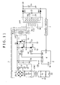
- FIG. 1 is a circuit diagram showing an example of configuration of a power supply circuit according to a first embodiment of the present invention
- FIG. 2 is a sectional view of an example of structure of a loosely coupled transformer
- FIGS. 3A , 3 B, 3 C, 3 D, 3 E, and 3 F are waveform charts showing operations of principal parts of the power supply circuit according to the first embodiment on the basis of a period of commercial alternating-current power supply;
- FIG. 4 is a diagram showing characteristics of a power factor, power conversion efficiency, and rectified and smoothed voltage level with respect to load variation in the power supply circuit according to the first embodiment
- FIG. 5 is a diagram showing characteristics of a power factor, power conversion efficiency, and rectified and smoothed voltage level with respect to variation of alternating input voltage in the power supply circuit according to the first embodiment
- FIG. 6 is a circuit diagram showing an example of configuration of a power supply circuit according to a second embodiment
- FIG. 7 is a circuit diagram showing an example of configuration of a power supply circuit according to a third embodiment
- FIGS. 8A , 8 B, 8 C, 8 D, and 8 E are waveform charts showing operations of principal parts of the power supply circuit according to the third embodiment on the basis of a period of commercial alternating-current power supply;
- FIG. 9 is a diagram showing characteristics of a power factor, power conversion efficiency, and rectified and smoothed voltage level with respect to load variation in the power supply circuit according to the third embodiment.
- FIG. 10 is a diagram showing characteristics of a power factor, power conversion efficiency, and rectified and smoothed voltage level with respect to variation of alternating input voltage in the power supply circuit according to the third embodiment
- FIG. 11 is a circuit diagram showing an example of configuration of a power supply circuit according to a fourth embodiment.
- FIG. 12 is a circuit diagram showing an example of configuration of a power supply circuit according to a fifth embodiment
- FIG. 13 is a sectional view of an example of structure of an isolated converter transformer according to the embodiment.
- FIG. 14 is a diagram of an equivalent circuit of the circuit shown in FIG. 12 (in the case of a coupling coefficient of 0.8 or lower of the isolated converter transformer);
- FIG. 15 is a diagram of an equivalent circuit of the circuit shown in FIG. 12 (in the case of a coupling coefficient of 0.90 or higher of the isolated converter transformer);
- FIG. 16 is a diagram showing characteristics of a power factor, power conversion efficiency, and rectified and smoothed voltage level with respect to load variation in the power supply circuit according to the fifth embodiment
- FIG. 17 is a circuit diagram showing an example of configuration of a power supply circuit according to a sixth embodiment.
- FIG. 18 is a circuit diagram showing a modification of the power supply circuit according to the sixth embodiment.
- FIG. 19 is a circuit diagram showing a modification of the power supply circuit according to the sixth embodiment.
- FIG. 20 is a diagram of an equivalent circuit of the circuit shown in FIG. 17 (in the case of a coupling coefficient of 0.8 or lower of the isolated converter transformer);
- FIG. 21 is a diagram of an equivalent circuit of the circuit shown in FIG. 17 (in the case of a coupling coefficient of 0.90 or higher of the isolated converter transformer);
- FIG. 22 is a diagram showing characteristics of a power factor, power conversion efficiency, and rectified and smoothed voltage level with respect to load variation in the power supply circuit according to the sixth embodiment
- FIG. 23 is a circuit diagram showing an example of configuration of a power supply circuit according to a seventh embodiment
- FIG. 24 is a circuit diagram showing a modification of the power supply circuit according to the seventh embodiment.
- FIG. 27 is a circuit diagram showing an example of configuration of a related art power supply circuit
- FIG. 28 is a diagram showing characteristics of a power factor, power conversion efficiency, and rectified and smoothed voltage level with respect to load variation in the power supply circuit shown in FIG. 27 ;
- FIG. 29 is a diagram showing characteristics of a power factor, power conversion efficiency, and rectified and smoothed voltage level with respect to variation of alternating input voltage in the power supply circuit shown in FIG. 27 ;
- FIG. 30 is a circuit diagram showing another example of configuration of a related art power supply circuit
- FIG. 31 is a diagram showing characteristics of a power factor, power conversion efficiency, and rectified and smoothed voltage level with respect to load variation in the power supply circuit shown in FIG. 30 ;
- FIG. 32 is a diagram showing characteristics of a power factor, power conversion efficiency, and rectified and smoothed voltage level with respect to variation of alternating input voltage in the power supply circuit shown in FIG. 30 .
- FIG. 1 shows an example of configuration of a switching power supply circuit according to a first embodiment of the present invention.
- the power supply circuit shown in this figure has a common-mode noise filter formed by connecting a common-mode choke coil CMC and one across capacitor CL to a commercial alternating-current power supply AC.
- the common-mode noise filter suppresses noise transmitted from a switching converter side to the commercial alternating-current power supply AC, for example.
- the power supply circuit employs a configuration in which a power factor improving circuit 3 formed with a rectifier circuit system included therein is connected to the commercial alternating-current power supply AC.
- the power factor improving circuit 3 includes a bridge rectifier circuit Di, a smoothing capacitor Ci, a filter capacitor CN, and a loosely coupled transformer VFT (power factor improving transformer).
- a positive electrode input terminal of the bridge rectifier circuit Di is connected to a positive electrode line of the commercial alternating-current power supply AC via a secondary winding N 12 of the loosely coupled transformer VFT connected in series with the positive electrode input terminal of the bridge rectifier circuit Di.
- a negative electrode input terminal of the bridge rectifier circuit Di is connected to a negative electrode line of the commercial alternating-current power supply AC.
- a positive electrode output terminal of the bridge rectifier circuit Di is connected to a positive electrode terminal of the smoothing capacitor Ci.
- a negative electrode terminal of the smoothing capacitor Ci is connected to a primary side ground.
- a positive electrode output terminal of the bridge rectifier circuit Di is connected to the primary side ground.
- a so-called full-wave rectification operation is obtained in which the smoothing capacitor Ci is charged with a rectified output rectified by the bridge rectifier circuit Di in each period of the alternating input voltage VAC supplied from the commercial alternating-current power supply AC being positive/negative. That is, a fundamental configuration of the rectifier circuit system is a full-wave rectifier circuit comprising one set of the bridge rectifier circuit and one set of the smoothing capacitor. The rectification operation of the full-wave rectifier circuit generates a rectified and smoothed voltage Ei having a level equal to that of the alternating input voltage VAC multiplied by unity across the smoothing capacitor Ci.
- a fast recovery type diode (high-frequency rectifier element) is selected as each of rectifier diodes (rectifier elements) Da to Dd forming the bridge rectifier circuit Di in the power factor improving circuit 3 .
- This provision is made for the rectifier diodes Da to Dd to switch rectification current as an operation for power factor improvement, as later described.
- the power supply circuit according to the present embodiment employs a circuit configuration in which the secondary winding N 12 of the loosely coupled transformer VFT is inserted in the positive electrode line of the commercial alternating-current power supply AC.
- an operation that increases a conduction angle of rectification current flowing through the rectifier circuit system is obtained, thus improving a power factor.
- the power factor improving operation of the power factor improving circuit 3 will be described later.
- FIG. 2 shows an example of structure of the loosely coupled transformer VFT.
- the loosely coupled transformer VFT has an E-E-shaped core formed by combining E-shaped cores CR 1 and CR 2 of ferrite material with each other in such a manner that magnetic legs of the core CR 1 are opposed to magnetic legs of the core CR 2 .
- a bobbin B is provided which is formed by a resin, for example, into a shape with a primary side winding part and a secondary side winding part divided from each other so as to be independent of each other.
- a primary winding N 11 is wound around one winding part of the bobbin B.
- the secondary winding N 12 is wound around the other winding part of the bobbin B.
- the bobbin B thus wound with the primary winding and the secondary winding is attached to the above-described E-E-shaped core (CR 1 and CR 2 ). Thereby the primary side winding and the secondary side winding are wound around the central magnetic leg of the E-E-shaped core in respective different winding regions.
- a structure of the loosely coupled transformer VFT as a whole is thus obtained.
- a gap G having a required gap length is formed at a junction part of the central magnetic leg. Thereby a state of loose coupling with a required coupling coefficient is obtained.
- the gap length of the gap G is about 1.5 mm, and the coupling coefficient is 0.75 or lower.
- the switching converter operating while receiving the rectified and smoothed voltage Ei as a direct-current input voltage in FIG. 1 employs the structure of a complex resonant converter in which the fundamental configuration of a current resonant converter is provided with at least a partial voltage resonant circuit on the primary side in this case.
- two switching devices Q 1 (high side) and Q 2 (low side) formed by a MOS-FET are connected to each other by half-bridge coupling.
- Damper diodes DD 1 and DD 2 are connected in a direction shown in the figure in parallel with the switching devices Q 1 and Q 2 between a drain—a source of the switching devices Q 1 and Q 2 , respectively.
- a partial resonant capacitor Cp is connected in parallel with the switching device Q 2 between the drain—the source of the switching device Q 2 .
- a capacitance of the partial resonant capacitor Cp and a leakage inductance L 1 of a primary winding N 1 form a parallel resonant circuit (a partial voltage resonant circuit).
- a partial voltage resonant operation in which voltage resonance occurs only when the switching devices Q 1 and Q 2 are turned off, is obtained.
- the partial voltage resonant circuit actually includes an inductance component L 11 of the primary winding N 11 of the loosely coupled transformer VFT which winding is connected in series with the primary winding N 1 of an isolated converter transformer PIT.
- a control IC 2 includes an oscillating circuit for driving the current resonant converter by an external excitation system, a control circuit, a protecting circuit and the like.
- the control IC 2 is a general-purpose analog IC (Integrated Circuit) having a bipolar transistor therewithin.
- the control IC 2 operates on a direct-current voltage (18 V) input to a power supply input terminal Vcc.
- the power supply input terminal Vcc is also connected with a line of the rectified and smoothed voltage Ei via a starting resistance RS.
- the control IC 2 is started by the rectified and smoothed voltage Ei input via the starting resistance RS at a time of a start of power supply.
- the control IC 2 is connected to the primary side ground by a grounding terminal E.
- the control IC 2 has two drive signal output terminals VGH and VGL as terminals for outputting drive signals (gate voltages) to the switching devices.
- the drive signal output terminal VGH outputs a drive signal for switching-driving the high side switching device.
- the drive signal output terminal VGL outputs a drive signal for switching-driving the low side switching device.
- the high side drive signal output from the drive signal output terminal VGH is applied to a gate of the switching device Q 1 .
- the low side drive signal output from the drive signal output terminal VGL is applied to a gate of the switching device Q 2 .
- a bootstrap circuit formed by a peripheral external part is actually connected to the control IC 2 .
- This bootstrap circuit is to shift level of the drive signal applied to the high side switching device Q 1 to a level at which the switching device Q 1 can be driven properly.
- the switching devices Q 1 and Q 2 are actually connected with part elements such as a gate resistance, a gate-to-source resistance and the like, though not shown in the figure.
- the control IC 2 generates an oscillating signal of a required frequency by the internal oscillating circuit. As later described, the oscillating circuit varies the frequency of the oscillating signal according to level of a control output input from a control circuit 1 to a terminal Vc.
- control IC 2 generates the high side drive signal and the low side drive signal using the oscillating signal generated by the oscillating circuit. Then, the control IC 2 outputs the high side drive signal from the drive signal output terminal VGH, and outputs the low side drive signal from the drive signal output terminal VGL.
- the high side drive signal and the low side drive signal have a waveform including an on period in which a rectangular pulse of positive polarity occurs and an off period of 0 V within one switching period.
- the high side drive signal and the low side drive signal both have the above-described waveform, and have output timing with a 180° phase difference from each other.
- Such waveforms are applied to the switching devices Q 1 and Q 2 , whereby the switching devices Q 1 and Q 2 perform switching operation so as to be turned on/off alternately.
- a short dead time in which both the switching devices Q 1 and Q 2 are turned off is formed in a period from the turning off of the switching device Q 1 to the turning on of the switching device Q 2 and in a period from the turning off of the switching device Q 2 to the turning on of the switching device Q 1 .
- This dead time is a period during which both the switching devices Q 1 and Q 2 are turned off.
- the dead time is formed to ensure charge and discharge operation at the partial resonant capacitor Cp in a short time in timing of the turning on/off of the switching devices Q 1 and Q 2 in partial voltage resonant operation.
- a time length as such a dead time can be set on the control IC 2 side, for example.
- the control IC 2 varies a pulse width duty ratio of the drive signals to be output from the drive signal output terminals VGH and VGL so as to form a period td of the set time length.
- the isolated converter transformer PIT transmits a switching output of the switching devices Q 1 and Q 2 to the secondary side.
- the primary winding N 1 and a secondary winding N 2 are wound in the isolated converter transformer PIT.
- one end of the primary winding N 1 of the isolated transformer PIT is connected to a point of connection (a switching output point) between the source of the switching device Q 1 and the drain of the switching device Q 2 via a series connection of the primary winding.
- N 11 of the loosely coupled transformer VFT and a series resonant capacitor C 1 is connected to the primary side ground.
- the series circuit of the series resonant capacitor C 1 the primary winding N 11 of the loosely coupled transformer VFT—the primary winding N 1 of the isolated converter transformer PIT is connected to the switching output point of the switching devices Q 1 and Q 2 .
- a capacitance of the series resonant capacitor C 1 , the leakage inductance L 1 of the isolated converter transformer PIT including the primary winding N 1 , and the inductance component L 11 of the primary winding N 11 of the loosely coupled transformer VFT form a primary side series resonant circuit.
- This primary side series resonant circuit is connected to the switching output point as described above, whereby the switching output of the switching devices Q 1 and Q 2 is transmitted to the primary side series resonant circuit.
- the primary side series resonant circuit performs resonant operation according to the transmitted switching output, and thereby converts the operation of the primary side switching converter into a current resonant type operation.
- the primary side switching converter shown in this figure obtains the current resonance type operation by the primary side series resonant circuit (C 1 -L 11 -L 1 ) and the partial voltage resonant operation by the partial voltage resonant circuit (Cp//L 1 (-L 11 )) described above.
- the power supply circuit shown in this figure employs a form in which the resonant circuit for making the primary side switching converter a resonant converter is combined with another resonant circuit. That is, the power supply circuit shown in the figure employs the configuration of a complex resonant converter.
- the structure of the isolated converter transformer PIT has an E-E-shaped core formed by combining E-shaped cores made of for example ferrite material with each other.
- the isolated converter transformer PIT has a primary side winding part and a secondary side winding part divided from each other.
- the primary winding N 1 and the secondary winding N 2 to be described next are wound around the central magnetic leg of the E-E-shaped core.
- a gap of about 1.0 mm to 1.5 mm is formed in the central magnetic leg of the E-E-shaped core. Thereby a state of loose coupling with a coupling coefficient of about 0.7 to 0.8 is obtained.
- the secondary winding N 2 is wound on the secondary side of the isolated converter transformer PIT. An alternating voltage corresponding to the switching output transmitted to the primary winding N 1 is induced in the secondary winding N 2 .
- the secondary winding N 2 is provided with a center tap, which is connected to a secondary side ground.
- a full-wave rectifier circuit comprising rectifier diodes D 01 and D 02 and a smoothing capacitor C 0 is connected to the secondary winding.
- a secondary side direct-current output voltage E 0 is obtained as a voltage across the smoothing capacitor C 0 .
- the secondary side direct-current output voltage E 0 is supplied to a load side not shown in the figure, and also inputted from a branch point as a detection voltage for a control circuit 1 to be described next.
- the control circuit 1 obtains, as a control output, a current or a voltage varied in level according to level of the secondary side direct-current output voltage E 0 . This control output is output to the control terminal Vc of the control IC 2 .
- the control IC 2 operates to vary the frequency of each of the high side drive signal and the low side drive signal to be output from the drive signal output terminals VGH and VGL in a synchronous state while retaining timing of turning on/off the drive signals alternately.
- the switching frequency of the switching devices Q 1 and Q 2 is variably controlled according to the level of the control output input to the control terminal Vc (that is, the level of the secondary side direct-current output voltage).
- the alternating input voltage VAC having a period as shown in FIG. 3A is obtained, for example, an alternating input current IAC flowing from the commercial alternating-current power supply.
- AC to a rectification current path flows so as to be of positive polarity/negative polarity in a positive/negative period, respectively, of the alternating input voltage VAC, as shown in FIG. 3B .
- a waveform shown in FIG. 3C is obtained as a potential V 1 between the primary side ground and a point of connection between the filter capacitor CN and an end part of the secondary winding N 12 of the loosely coupled transformer VFT in a line of the commercial alternating-current power supply AC.
- a waveform shown in FIG. 3E is obtained as a potential V 2 between the positive electrode input terminal of the bridge rectifier circuit Di and the primary side ground.
- the switching output of the primary side switching converter is transmitted to the primary winding N 11 in the loosely coupled transformer VFT.
- An alternating voltage is correspondingly induced in the secondary winding N 12 of the loosely coupled transformer VFT. Since as also described above, the secondary winding N 12 of the loosely coupled transformer VFT is inserted in a rectification current path, an operation of voltage feedback of the switching output of the primary side switching converter to the rectification current path is obtained by the loosely coupled transformer VFT.
- the potentials V 1 and V 2 shown in FIGS. 3C and 3E have an alternating waveform component superimposed thereon in periods other than conduction periods of the alternating input current IAC, as shown in the figures. This results from the voltage feedback of the switching output of the primary side switching converter as described above.
- a current I 2 flowing from the line of the commercial alternating-current power supply AC to the secondary winding N 12 of the loosely coupled transformer VFT flows in a steady alternating waveform as shown in FIG. 3F .
- This current I 2 is obtained as a waveform having a fixed amplitude with a zero level as a center and having a component of a rectified current I 1 of positive polarity superimposed thereon so as to correspond to the conduction periods of the alternating input current IAC.
- the rectified current I 1 flows from the filter capacitor CN through the positive electrode line of the commercial alternating-current power supply AC to a rectification current path of the secondary winding N 12 ⁇ the rectifier diode Da of the bridge rectifier circuit Di ⁇ the smoothing capacitor Ci ⁇ the primary side ground ⁇ the rectifier diode Dd ⁇ the negative electrode line of the commercial alternating-current power supply AC.
- the rectified current I 1 flows from the filter capacitor CN through the negative electrode line of the commercial alternating-current power supply AC to a rectification current path of the rectifier diode Dc ⁇ the smoothing capacitor Ci ⁇ the primary side ground ⁇ the rectifier diode Db ⁇ the secondary winding N 12 .
- the rectified current is interrupted so as to be switched by the fast recovery type rectifier diodes (Da to Dd), whereby a charging current flows to the smoothing capacitor Ci even in a period when a rectification output voltage level is lower than level of the rectified and smoothed voltage Ei.
- an average waveform of the alternating input current approaches a waveform of the alternating input voltage, whereby as shown in FIG. 3B , a conduction angle of the alternating input current IAC is increased. As a result of the increase in the conduction angle of the alternating input current IAC, a power factor is improved.
- the filter capacitor CN 1 ⁇ F
- the primary winding N 1 of the isolated converter transformer PIT 32 T
- the primary side series resonant capacitor C 1 0.068 ⁇ F
- the primary side partial resonant capacitor Cp 680 pF
- the inductance L 11 of the primary winding N 11 75 ⁇ H
- the inductance L 12 of the primary winding N 12 50 ⁇ H
- the present embodiment obtains the rectified and smoothed voltage Ei having a level higher than 134 V.
- Such an increase in the rectified and smoothed voltage Ei is obtained by superimposing an amount of voltage feedback of the switching output as the rectified and smoothed voltage Ei.
- the power choke coil PCH is omitted, and the loosely coupled transformer VFT is provided instead.
- the power choke coil PCH in the circuit shown in FIG. 27 has a weight of 153 g and a board occupying area of 11 cm 2 .
- a combination of the loosely coupled transformer VFT and the filter capacitor CN in the circuit shown in FIG. 1 has a weight of 48 g, which represents a reduction to about 31% of that of the power choke coil PCH in the circuit shown in FIG. 27 .
- the board occupying area is 9 cm 2 , which represents a reduction to about 82%.
- the power choke coil PCH is omitted, it is not necessary to consider effects of a leakage flux caused by the power choke coil PCH on a load side. This eliminates the need for a measure of providing a magnetic shield sheet to the power choke coil PCH, for example, and thus also contributes to reduction in size and weight of the circuit.
- FIG. 6 shows an example of configuration of a switching power supply circuit according to a second embodiment of the present invention.
- a parallel resonant capacitor C 2 is connected in parallel with a secondary winding N 2 of an isolated converter transformer PIT.
- a capacitance of the parallel resonant capacitor C 2 and a leakage inductance L 2 of the secondary winding N 2 form a secondary side parallel resonant circuit.
- the capacitance of the parallel resonant capacitor C 2 is selected to be 1000 pF to 3300 pF.
- the secondary side parallel resonant circuit is formed as a voltage resonant circuit for converting operation of a secondary side rectifier circuit into a voltage resonant type operation, or a partial voltage resonant circuit for obtaining a partial voltage resonant operation.
- the power supply circuit according to the second embodiment has a resonant circuit also on the secondary side as a complex resonant converter.
- the power factor improving circuit 3 of the power supply circuit shown in FIG. 6 has fast recovery type rectifier diodes (high-frequency rectifier elements) D 1 , D 2 , and D 3 added thereto as component parts. That is, in this case, rectification current is not interrupted by switching by rectifier diodes of a bridge rectifier circuit Di. As diodes for switching rectification current in a rectification current path, the rectifier diodes D 1 , D 2 , and D 3 are provided.
- the rectifier diodes Da to Dd of the bridge rectifier circuit Di in this case are a slow recovery type (low-frequency rectifier elements) because the rectifier diodes Da to Dd do not switch rectification current.
- a positive electrode input terminal of the bridge rectifier circuit Di in this case is directly connected to a commercial alternating-current power supply AC.
- the positive electrode input terminal of the bridge rectifier circuit Di is connected from a secondary winding N 12 of a loosely coupled transformer VFT, which winding is connected in series with the positive electrode input terminal of the bridge rectifier circuit Di, through an anode ⁇ a cathode of the rectifier diode D 1 to a positive electrode terminal of a smoothing capacitor Ci.
- the rectifier diode D 2 has a cathode connected to the anode of the rectifier diode D 1 , and an anode connected to a primary side ground.
- a positive electrode output terminal of the bridge rectifier circuit Di is connected through an anode ⁇ a cathode of the rectifier diode D 3 to the positive electrode terminal of the smoothing capacitor Ci.
- a filter capacitor CN in this case is inserted between the positive electrode input terminal of the bridge rectifier circuit Di and the positive electrode terminal of the smoothing capacitor Ci (a point of connection between the anodes of the rectifier diodes D 1 and D 3 ).
- the filter capacitor CN forms a current path for a high-frequency component obtained by switching rectification current flowing as described next.
- An alternating input current IAC in the power factor improving circuit 3 is branched into a first rectification current I 1 flowing from a positive electrode line of the commercial alternating-current power supply AC to the diode Da forming the bridge rectifier circuit Di and a second rectification current I 2 flowing from the positive electrode line of the commercial alternating-current power supply AC to the secondary winding N 12 of the loosely coupled transformer VFT.
- the first rectification current I 1 flows in a path of the positive electrode line of the commercial alternating-current power supply AC ⁇ the rectifier diode Da (the bridge rectifier circuit Di) ⁇ the rectifier diode D 3 ⁇ the smoothing capacitor Ci ⁇ the rectifier diode Dd (the bridge rectifier circuit Di) ⁇ a negative electrode line of the commercial alternating-current power supply AC.
- the second rectification current I 2 branches off from the positive electrode line of the commercial alternating-current power supply AC to flow in a path of the secondary winding N 12 (the loosely coupled transformer VFT) ⁇ the rectifier diode D 1 and then flow into the smoothing capacitor Ci.
- the first rectification current I 1 flows in a path of the negative electrode line of the commercial alternating-current power supply AC ⁇ the rectifier diode Dc (the bridge rectifier circuit Di) ⁇ the rectifier diode D 3 ⁇ the smoothing capacitor Ci ⁇ the rectifier diode Db (the bridge rectifier circuit Di) ⁇ the positive electrode line of the commercial alternating-current power supply AC.
- the second rectification current I 2 flows in a path of the negative electrode line of the commercial alternating-current power supply AC ⁇ the rectifier diode Dc (the bridge rectifier circuit Di) ⁇ the rectifier diode D 1 ⁇ the smoothing capacitor Ci, and thereafter branches off to flow in a path of the rectifier diode D 2 ⁇ the secondary winding N 12 (the loosely coupled transformer VFT) ⁇ the positive electrode line of the commercial alternating-current power supply AC.
- the power factor improving circuit 3 voltage feedback of switching output is performed by an alternating voltage induced in the secondary winding N 12 of the loosely coupled transformer VFT.
- the first rectification current I 1 is switched by the fast recovery type rectifier diode D 3 and the second rectification current I 2 is switched by the fast recovery type rectifier diodes D 1 and D 2 (and D 3 ).
- the rectification currents thereby form an alternating waveform.
- a high-frequency current component thus obtained as alternating waveform with a switching period is absorbed so as to charge and discharge the filter capacitor CN, whereby normal-mode noise is suppressed.
- the power supply circuit shown in FIG. 6 can also improve power conversion efficiency and reduce circuit board size and weight.
- the rectifier diode D 3 inserted between the positive electrode output terminal of the bridge rectifier circuit Di and the positive electrode of the smoothing capacitor Ci operates to switch and pass the rectification current only in the vicinity of substantially a peak level of the alternating input voltage VAC, for example. This controls a peak level of the rectification current flowing on a side of the rectifier diodes D 1 and D 2 , the peak level occurring in accordance with a peak of the alternating input voltage VAC. It is therefore possible to reduce a switching loss in the rectifier diodes D 1 and D 2 and attendant heat generation.
- the power supply circuit shown in this figure has a voltage doubler rectifier circuit as a fundamental configuration of a rectifier circuit system provided within a power factor improving circuit 3 .
- two smoothing capacitors Ci 1 –Ci 2 connected in series with each other are provided, and the series circuit of the smoothing capacitors Ci 1 and Ci 2 is inserted in parallel between a positive electrode output terminal of a bridge rectifier circuit Di and a primary side ground.
- a negative electrode line of a commercial alternating-current power supply AC is connected to a point of connection between the smoothing capacitors Ci 1 –Ci 2 .
- a negative electrode input terminal of the bridge rectifier circuit Di is connected to a positive electrode input terminal of the same bridge rectifier circuit Di so that rectifier diodes Da and Dc forming the bridge rectifier circuit Di are connected in parallel with each other in a rectification current path.
- the rectifier diodes Da to Dd of the bridge rectifier circuit Di in this case are of a fast recovery type for switching rectification current.
- the thus formed voltage doubler rectifier circuit generates a rectified and smoothed voltage Ei (direct-current input voltage) corresponding to twice a level of the alternating input voltage VAC by rectifying operation to be described later.
- the voltage doubler rectifier circuit raises the level of the rectified and smoothed voltage Ei to thereby meet the condition of a heavier load than the circuits shown in FIG. 1 and FIG. 6 , for example.
- a power factor improving operation of the above-described power factor improving circuit 3 will be described with reference to waveform charts of FIGS. 8A , 8 B, 8 C, 8 D, and 8 E. Together with the power factor improving operation of the power factor improving circuit 3 , rectifying operation of the voltage doubler rectifier circuit included in the power factor improving circuit 3 will also be described in the following.
- a potential V 1 shown in FIG. 8C forms a sine wave having a maximum value in a positive period of the alternating input voltage VAC and a minimum value of 0 V in a negative period of the alternating input voltage VAC, as shown in the figure.
- This potential V 1 is a potential between the primary side ground and a point of connection between a filter capacitor CN and a secondary winding N 12 of a loosely coupled transformer VFT in a positive electrode line of the commercial alternating-current power supply AC as a path in which second rectification current I 2 flows, as shown in the figure.
- the second rectification current I 2 flows on the basis of the alternating input current IAC in each positive/negative period in which an absolute value of the alternating input voltage VAC is higher than an absolute value of the potential V 1 shown in FIG. 8C .
- the second rectification current I 2 flows in an alternating waveform shown in the figure with positive polarity/negative polarity in each positive polarity/negative polarity period, respectively, of the alternating input voltage VAC.
- the second rectification current I 2 flows from the filter capacitor CN through the secondary winding N 12 of the loosely coupled transformer VFT via the positive electrode line of the commercial alternating-current power supply AC, and further flows through the parallel circuit of the rectifier diodes Da//Dc of the bridge rectifier circuit Di. Then, passing through the parallel circuit of the rectifier diodes Da//Dc, the current flows into a positive electrode terminal ⁇ a negative electrode terminal of the smoothing capacitor Ci 1 as first rectification current I 1 , and further flows from the negative electrode line of the commercial alternating-current power supply AC into the filter capacitor CN.
- the second rectification current flows from the filter capacitor CN through the negative electrode line of the commercial alternating-current power supply AC to a positive electrode terminal ⁇ a negative electrode terminal of the smoothing capacitor Ci 2 , and further flows through the rectifier diode Db of the bridge rectifier circuit Di via the primary side ground. Then, passing through the rectifier diode Db, the second rectification current I 2 flows from the positive electrode line of the commercial alternating-current power supply AC through the secondary winding N 12 of the loosely coupled transformer VFT into the filter capacitor CN.
- the smoothing capacitor Ci 1 is charged in a period of positive polarity of the alternating input voltage VAC, and thus a rectified and smoothed voltage having a level equal to that of the alternating input voltage VAC multiplied by unity is obtained at the smoothing capacitor Ci 1 .
- the smoothing capacitor Ci 2 is charged, and thus a rectified and smoothed voltage having a level equal to that of the alternating input voltage VAC multiplied by unity is also obtained at the smoothing capacitor Ci 2 .
- the second rectification current I 2 is passed through the parallel circuit of the rectifier diodes (Da//Dc).
- the power supply circuit shown in FIG. 7 deals with the condition of a heavier load than the power supply circuits according to the embodiments shown in FIG. 1 and FIG. 6 . That is, while an amount of rectification current increases as the load becomes heavier, the amount of current flowing through the rectifier diodes is reduced when the rectification current is passed through the rectifier diodes in parallel. It is therefore possible to correspondingly reduce a load on the rectifier diodes.
- an alternating voltage is induced in the secondary winding N 12 of the loosely coupled transformer VFT, and thus an alternating voltage component with a switching period is superimposed on a rectification current path. That is, voltage feedback of switching output to the rectification current path is performed. Since the alternating voltage component with a switching period is superimposed, the rectifier diodes of the bridge rectifier circuit Di obtain an operation of switching the rectification current.
- the rectification current forms an alternating waveform flowing in a direction of negative polarity.
- the filter capacitor CN 1 ⁇ F
- a primary winding N 1 of an isolated converter transformer PIT 35 T
- a secondary winding N 2 of the isolated converter transformer PIT 25 T+25 T (turns) with a center tap as a dividing position
- a primary side series resonant capacitor C 1 0.039 ⁇ F
- a primary side partial resonant capacitor Cp 680 pF
- An inductance L 12 of the primary winding N 12 100 ⁇ H
- the present embodiment obtains the rectified and smoothed voltage Ei having a level higher than 264 V.
- the power choke coil PCH is omitted, and the loosely coupled transformer VFT is provided instead.
- the power choke coil PCH in the circuit shown in FIG. 30 has a weight of 240 g and a board occupying area of 19 cm 2 .
- the loosely coupled transformer VFT and the filter capacitor CN in the circuit shown in FIG. 7 has a total weight of 48 g and the loosely coupled transformer VFT has a board occupying area of 9 cm 2 .
- the weight is reduced to about 20%, and the occupying area is greatly reduced to about 47%.
- the power supply circuit of FIG. 7 also eliminates the need for a measure of providing a magnetic shield sheet or the like considering effects of a leakage flux caused by the power choke coil PCH on a load side.
- FIG. 11 shows an example of configuration of a power supply circuit according to a fourth embodiment of the present invention.
- a rectified and smoothed voltage Ei obtained across smoothing capacitors Ci 1 –Ci 2 connected in series with each other has a level corresponding to twice the alternating input voltage VAC.
- a slow recovery type rectifier diode is selected as rectifier diodes Da to Dd forming a bridge rectifier circuit Di shown in FIG. 11 . That is, in this case, the rectifier diodes of the bridge rectifier circuit Di do not interrupt rectification current by switching.
- fast recovery type rectifier diodes D 1 and D 2 are provided as a diode for switching rectification current in a rectification current path.
- a positive electrode input terminal of the bridge rectifier circuit Di in this case is connected to a point of connection between a positive electrode line of a commercial alternating-current power supply AC and a filter capacitor CN.
- the positive electrode input terminal of the bridge rectifier circuit Di is also connected to a positive electrode terminal of the smoothing capacitor Ci 1 via a secondary winding N 12 of a loosely coupled transformer VFT—the rectifier diode D 1 (an anode ⁇ a cathode).
- the rectifier diode D 2 has an anode connected to a primary side ground, and a cathode connected to the cathode of the rectifier diode D 2 .
- a negative electrode input terminal of the bridge rectifier circuit Di in this case is also connected to the positive electrode input terminal of the same bridge rectifier circuit Di, whereby a parallel circuit of the rectifier diodes Da//Dc is formed within a rectification current path formed as later described.
- a rectification current in a period of positive polarity of the alternating input voltage VAC branches off into a component of a first rectification current I 1 flowing from the line of the commercial alternating-current power supply AC through a path of the rectifier diode Da ⁇ the smoothing capacitor Ci 1 ⁇ a negative electrode line of the commercial alternating-current power supply AC and a component of a second rectification current I 2 flowing through a path of the secondary winding N 12 of the loosely coupled transformer VFT ⁇ the rectifier diode D 1 ⁇ the smoothing capacitor Ci 1 ⁇ the negative electrode line of the commercial alternating-current power supply AC ⁇ the filter capacitor CN.
- the rectifier diode D 1 performs switching on the basis of an alternating waveform induced in the secondary winding N 12 of the loosely coupled transformer VFT, and thus the second rectification current I 2 forms an alternating waveform.
- the rectification current first flows from a side of the negative electrode line of the commercial alternating-current power supply AC to the smoothing capacitor Ci 2 . Thereafter the rectification current branches off into a path of the rectifier diode Db ⁇ the positive electrode line of the commercial alternating-current power supply AC and a path of the rectifier diode D 2 ⁇ the secondary winding N 12 of the loosely coupled transformer VFT ⁇ the positive electrode line of the commercial alternating-current power supply AC ⁇ the filter capacitor CN.
- the rectification current flowing in the latter path is the second rectification current I 2 in this case.
- the rectification current flowing in the former path does not form an alternating waveform because the rectifier diode Db does not perform switching.
- the rectifier diode D 2 performs switching on the basis of the alternating waveform induced in the secondary winding N 12 of the loosely coupled transformer VFT, and thus the second rectification current I 2 flowing in the latter path forms an alternating waveform.
- the path in which the rectification current flows through a required rectifier diode of the bridge rectifier circuit Di and a path in which the rectification current flows through the fast recovery type rectifier diode D 1 or D 2 form path portions in which the rectification current branches off to flow in parallel.
- the rectification current flowing in the path on a side of the fast recovery type rectifier diode D 1 or D 2 is switched by the rectifier diode D 1 or D 2 .
- the smoothing capacitor Ci 1 is charged in a period of positive polarity of the alternating input voltage VAC
- the smoothing capacitor Ci 2 is charged in a period of negative polarity of the alternating input voltage VAC.
- the rectifying operation is a voltage doubler rectifier operation that generates a rectified and smoothed voltage Ei corresponding to twice a level of the alternating input voltage VAC as voltage across the series connection circuit of the smoothing capacitors Ci 1 –Ci 2 .
- the power supply circuit shown in FIG. 11 has a parallel resonant capacitor C 2 connected in parallel with a secondary winding N 2 of an isolated converter transformer PIT.
- a capacitance of the parallel resonant capacitor C 2 and a leakage inductance L 2 of the secondary winding N 2 form a voltage resonant circuit for converting operation of a secondary side rectifier circuit into a voltage resonant type operation, or a partial voltage resonant circuit for obtaining a partial voltage resonant operation.
- such a secondary side voltage resonant circuit may be provided in the power supply circuits according to the first and third embodiments shown in FIG. 1 and FIG. 7 .
- a secondary side series resonant circuit (current resonant circuit) formed by connecting a resonant capacitor in series with the secondary winding N 2 , for example, may be provided.
- FIG. 12 shows a configuration of a power supply circuit according to a fifth embodiment of the present invention.
- the same parts as in FIG. 1 , FIG. 6 , FIG. 7 , and FIG. 11 are identified by the same reference numerals, and description thereof will be omitted.
- the power supply circuit shown in this figure has a drive control circuit 4 .
- This circuit is for example formed by integrating the control circuit 1 and the control IC 2 provided in the circuit diagram of the power supply circuit according to each of the embodiments described earlier into one circuit part.
- a full-wave rectifier circuit comprising a bridge rectifier circuit Di and one smoothing capacitor Ci is formed in a power factor improving circuit 3 shown in this figure.
- a slow recovery type rectifier diode is selected as each of rectifier diodes Da to Dd forming the bridge rectifier circuit Di.
- a positive electrode input terminal of the bridge rectifier circuit Di (a point of Da-Db connection) is connected to a point of connection between a common mode choke coil CMC and a filter capacitor CN on a side of a positive electrode line of a commercial alternating-current power supply AC.
- the positive electrode input terminal of the bridge rectifier circuit Di is also connected to a positive electrode terminal of the smoothing capacitor Ci (a positive electrode line of a rectified and smoothed voltage Ei) via a series connection of a secondary winding N 12 of the loosely coupled transformer VFT for power factor improvement—the rectifier diode D 1 (an anode ⁇ a cathode).
- This series connection of the secondary winding N 12 of the loosely coupled transformer VFT—the rectifier diode D 1 can be considered to be connected in parallel with the rectifier diode Da of the bridge rectifier circuit Di.
- a positive electrode output terminal of the bridge rectifier circuit Di (a point of Da-Dc connection) is connected to the positive electrode terminal of the smoothing capacitor Ci.
- a negative electrode input terminal of the bridge rectifier circuit Di (a point of Dc-Dd connection) is connected to a point of connection between the common mode choke coil CMC and the filter capacitor CN on a side of a negative electrode line of the commercial alternating-current power supply AC.
- a negative electrode output terminal of the bridge rectifier circuit Di is connected to a primary side ground.
- a point of connection between the secondary winding N 12 of the loosely coupled transformer VFT and the anode of the rectifier diode D 1 is connected with a cathode of the rectifier diode D 2 .
- An anode of the rectifier diode D 2 is connected to the primary side ground.
- a rectification current in a period of positive polarity of the alternating input voltage VAC branches off into a component of a first rectification current I 1 flowing through a rectification current path of the positive electrode line of the commercial alternating-current power supply AC ⁇ the rectifier diode Da ⁇ the smoothing capacitor Ci ⁇ the rectifier diode Dd ⁇ the negative electrode line of the commercial alternating-current power supply AC and a component of a second rectification current I 2 flowing through a rectification current path of the positive electrode line of the commercial alternating-current power supply AC ⁇ the secondary winding N 12 of the loosely coupled transformer VFT ⁇ the rectifier diode D 1 ⁇ the smoothing capacitor Ci ⁇ the rectifier diode Dd ⁇ the negative electrode line of the commercial alternating-current power supply AC ⁇ the filter capacitor CN.
- the rectifier diodes Da and Dd that perform rectification in the rectification current path in which the first rectification current flows are of a slow recovery type, and does not perform switching operation with a switching period. Therefore the first rectification current does not form an alternating waveform.
- the rectifier diode D 1 switches the rectification current on the basis of an alternating voltage induced in the secondary winding N 12 of the loosely coupled transformer VFT.
- the second rectification current forms an alternating waveform, and flows into the smoothing capacitor Ci.
- the rectification current branches into the first rectification current flowing through a rectification current path of the negative electrode line of the commercial alternating-current power supply AC ⁇ the rectifier diode Dc ⁇ the smoothing capacitor Ci ⁇ the rectifier diode Db ⁇ the positive electrode line of the commercial alternating-current power supply AC and the second rectification current flowing through a path of the negative electrode line of the commercial alternating-current power supply AC ⁇ the rectifier diode Dc ⁇ the smoothing capacitor Ci ⁇ the rectifier diode D 2 ⁇ the secondary winding N 12 of the loosely coupled transformer VFT ⁇ the negative electrode line of the commercial alternating-current power supply AC ⁇ the filter capacitor CN.
- the rectifier diodes Dc and Db that rectify the first rectification current in the period of negative polarity of the alternating input voltage VAC are of a slow recovery type, and does not perform switching operation. Therefore the first rectification current does not form an alternating waveform.
- the second rectification current is switched by the fast recovery type rectifier diode D 2 that performs switching operation on the basis of the alternating voltage induced in the secondary winding N 12 of the loosely coupled transformer VFT.
- the second rectification current forms an alternating waveform.
- the rectification current is switched to form an alternating waveform according to a switching output fed back by voltage feedback of the loosely coupled transformer VFT.
- the loosely coupled transformer VFT provided in the power supply circuit according to the fifth embodiment shown in FIG. 12 it suffices for the loosely coupled transformer VFT provided in the power supply circuit according to the fifth embodiment shown in FIG. 12 to employ the structure shown in FIG. 2 .
- the length of a gap formed in a central magnetic leg of an E-E-shaped core in the loosely coupled transformer VFT is set at about 1 mm, and a coefficient of coupling between a primary winding N 11 and the secondary winding N 12 is set at about 0.8.
- the coupling coefficient is set at 0.75 or lower, and the gap length is set at about 1.5 mm.
- Such a change in the coupling coefficient of the loosely coupled transformer VFT in the present embodiment is related to a coupling coefficient set in an isolated converter transformer PIT. This point will be described.
- FIG. 14 shows an equivalent circuit of the power supply circuit shown in FIG. 12 when a state of loose coupling is set with a coupling coefficient of about 0.7 to 0.8 as a coefficient of coupling between a primary winding N 1 and a secondary winding N 2 side of the isolated converter transformer PIT as in each of the foregoing embodiments.
- an inductance (LN 11 ) of the primary winding N 11 of the loosely coupled transformer VFT can be represented as a series connection of an exciting inductance Le 11 and a leakage inductance Lk 11 of the primary winding N 11 .
- an inductance (LN 1 ) of the primary winding N 1 of the isolated converter transformer PIT can be represented as a series connection of an exciting inductance Le 1 and a leakage inductance Lk 1 of the primary winding N 1 .
- the primary winding N 1 of the isolated converter transformer PIT and the primary winding N 11 of the loosely coupled transformer VFT are connected in series with each other within a primary side series resonant circuit.
- an inductance when the isolated converter transformer PIT is viewed from the primary side is represented as a series connection of the exciting inductance Le 11 of the primary winding N 11 , the leakage inductance Lk 11 of the primary winding N 11 , and the leakage inductance Lk 1 of the primary winding N 1 .
- an equivalent leakage inductance when the isolated converter transformer PIT is viewed from the primary side is represented as
- the coupling coefficient between the primary side and the secondary side when viewed as that of the power supply circuit as a whole is 0.8 or lower.
- a product having a correspondingly high withstand voltage needs to be selected as the smoothing capacitor (Ci) for generating the rectified and smoothed voltage Ei (direct-current input voltage), switching devices (Q 1 and Q 2 ), a primary side series resonant capacitor C 1 and the like.
- This invites an increase in size and weight of a circuit board which increase accompanies an increase in size of part elements and an increase in cost.
- the increase in the direct-current input voltage as the load becomes lighter means a wide range of variation of the direct-current input voltage.
- a switching frequency control range for achieving constant voltage is extended, and a control range is reduced.
- secondary side direct-current output voltage controlled to be constant may be degraded in terms of transient response characteristics between a maximum load and a light load.
- the present embodiment is configured such that the isolated converter transformer PIT singly has a coupling coefficient of 0.90 or higher.
- the structure of the isolated converter transformer PIT has an E-E-shaped core formed by combining E-shaped cores CR 11 and CR 12 made of ferrite material with each other such that magnetic legs of the core CR 11 are opposed to magnetic legs of the core CR 12 .
- the isolated converter transformer PIT also has a bobbin B formed by resin, for example, and having a shape such that a primary side winding part and a secondary side winding part are divided so as to be independent of each other.
- the primary winding N 1 is wound around one winding part of the bobbin B.
- the secondary winding N 2 is wound around the other winding part of the bobbin B.
- the bobbin B thus wound with the primary winding and the secondary winding is attached to the E-E-shaped core (CR 11 and CR 12 ). Thereby the primary side winding and the secondary side winding are wound around the central magnetic leg of the E-E-shaped core in respective different winding regions.
- the structure of the isolated converter transformer PIT as a whole is thus obtained.
- a coupling coefficient of 0.90 or higher is obtained by setting gap length of a gap G formed at a junction part of the central magnetic leg.
- FIG. 15 shows an equivalent circuit of the power supply circuit of FIG. 12 when the coupling coefficient of the isolated converter transformer PIT is thus set to 0.90 or higher.
- the part of the series connection circuit of the primary winding N 1 of the isolated converter transformer PIT and the primary winding N 11 of the loosely coupled transformer VFT can be considered to have one leakage inductance component (Lk 11 +LK 1 ) connected in series between the exciting inductance Le 1 of the primary winding N 1 of the isolated converter transformer PIT and the exciting inductance Le 11 of the primary winding N 11 of the loosely coupled transformer VFT.
- the gap length 0.4 mm
- the primary winding N 1 22 T
- the secondary winding N 2 14 T+14 T with a center tap as a dividing position
- the leakage inductance LK 1 of the primary winding N 1 of the isolated converter transformer PIT 49 ⁇ H
- the leakage inductance LK 2 of the primary winding N 1 of the isolated converter transformer PIT 17 ⁇ H
- the loosely coupled transformer VFT has a coupling coefficient of about 0.8 as described above.
- the loosely coupled transformer VFT in practice has an EE-28 ferrite core, a gap length set to 1 mm, and a coupling coefficient of 0.79, the following inductance values are obtained.
- the power supply circuit as a whole configured as shown in FIG. 12 which circuit is represented as the equivalent circuit of FIG. 15 has a coupling coefficient of 0.84.
- a coupling coefficient higher than 0.80 is obtained.
- 0.039 ⁇ F is selected for the primary side series resonant capacitor C 1 .
- the range of variation is sufficiently reduced. That is, a phenomenon in which the rectified and smoothed voltage Ei (direct-current input voltage) is increased greatly as the load becomes lighter does not occur because a required value or higher (for example 0.8 or higher) is retained as the coupling coefficient of the circuit as a whole.
- a range of load variation is different, a comparison with FIG. 4 showing the characteristics of the power supply circuit according to the foregoing first embodiment, for example, indicates that a curve in a range of load variation in which the load is light (a range where the load power Po is about 100 W or lower in FIG. 16 , for example) is gentler. That is, a decrease in the power conversion efficiency under light-load conditions is suppressed.
- the smoothing capacitor Ci the switching devices (Q 1 and Q 2 ), the primary side series resonant capacitor C 1 and the like in the power supply circuit shown in FIG. 12 do not need to have a high withstand voltage. This makes it possible to reduce the size and weight of the circuit board and reduce the cost.
- the coupling coefficient is set to 0.8 or lower, for example, the number of turns of the primary winding N 1 needs to be about 33 T.
- the power supply circuit according to the fifth embodiment has a parallel resonant capacitor C 2 connected in parallel with the secondary winding N 2 of the isolated converter transformer PIT.
- a capacitance of the parallel resonant capacitor C 2 and a leakage inductance L 2 of the secondary winding N 2 form a secondary side parallel resonant circuit.
- the secondary side parallel resonant circuit is formed as a voltage resonant circuit for converting operation of a secondary side rectifier circuit into a voltage resonant type operation, or a partial voltage resonant circuit for obtaining a partial voltage resonant operation.
- the circuit configuration shown in FIG. 1 is used as the power factor improving circuit 3 in place of the configuration shown in FIG. 12 .
- the coupling coefficients of the isolated converter transformer PIT and the loosely coupled transformer VFT are set as described above, whereby the power supply circuit according to the fifth embodiment is obtained.
- the coupling coefficients of the isolated converter transformer and the power factor improving transformer are set so as to obtain a required coupling coefficient of the circuit as a whole, and the isolated converter transformer in particular has a required coupling coefficient set therein that does not represent loose coupling, whereby the range of variation of the direct-current input voltage (rectified and smoothed voltage) according to load variation is reduced.
- This also suppresses a decrease in power conversion efficiency, or facilitates an improvement in power conversion efficiency, and further extends a constant voltage control range.
- a power supply circuit according to a sixth embodiment will next be described.
- the power supply circuit according to the sixth embodiment is based on the configuration of the power supply circuit according to the foregoing fifth embodiment.
- FIG. 17 shows an example of configuration of the power supply circuit according to the sixth embodiment.
- the same parts as in the figures showing the configurations of the power supply circuits according to the first to fifth embodiments are identified by the same reference numerals, and description thereof will be omitted.
- the power factor improving circuit 3 of the power supply circuit shown in this figure is provided with a voltage doubler rectifier circuit to deal with the 100 V system of the commercial alternating-current power supply AC.
- a bridge rectifier circuit Di comprises slow recovery type rectifier diodes Da and Db.
- the rectifier diode Da has an anode connected to a point of connection between a common mode choke coil CMC and a filter capacitor CN on a side of a positive electrode line of the commercial alternating-current power supply AC, and has a cathode connected to a positive electrode terminal of a smoothing capacitor Ci 1 (a positive electrode line of a rectified and smoothed voltage Ei).
- the rectifier diode Db has an anode connected to a primary side ground, and a cathode connected to the anode of the rectifier diode Da.
- two smoothing capacitors Ci 1 ⁇ Ci 2 connected in series with each other are provided.
- the positive electrode terminal of the smoothing capacitor Ci 1 is connected to the cathode of the rectifier diode Da, as described above.
- a negative electrode terminal of the smoothing capacitor Ci 2 is connected to the primary side ground.
- a point of connection between a negative electrode terminal of the smoothing capacitor Ci 1 and a positive electrode terminal of the smoothing capacitor Ci 2 is connected to a point of connection between the common mode choke coil CMC and the filter capacitor CN on a side of a negative electrode line of the commercial alternating-current power supply AC.
- a series circuit of a secondary winding N 12 of a loosely coupled transformer VFT and a fast recovery type rectifier diode D 1 is connected between the positive electrode terminal of the smoothing capacitor Ci 1 (the positive electrode line of the rectified and smoothed voltage Ei) and the point of connection between the common mode choke coil CMC and the filter capacitor CN on the side of the positive electrode line of the commercial alternating-current power supply AC.
- the rectifier diode D 1 has an anode connected to the secondary winding N 12 , and a cathode connected to the positive electrode terminal of the smoothing capacitor Ci 1 .
- a point of connection between the anode of the rectifier diode D 1 and the secondary winding N 12 of the loosely coupled transformer VFT is connected with a cathode of a fast recovery type rectifier diode D 2 .
- An anode of the rectifier diode D 2 is connected to the primary side ground.
- a first rectification current I 1 flows from the positive electrode line of the commercial alternating-current power supply AC through a path of the rectifier diode Da ⁇ the smoothing capacitor Ci 1 ⁇ the negative electrode line of the commercial alternating-current power supply AC.
- a second rectification current I 2 flows from the positive electrode line of the commercial alternating-current power supply AC through a path of the secondary winding N 12 of the loosely coupled transformer VFT ⁇ the rectifier diode D 1 ⁇ the smoothing capacitor Ci 1 ⁇ the negative electrode line of the commercial alternating-current power supply AC ⁇ the filter capacitor CN.
- the first rectification current does not form an alternating waveform because the slow recovery type rectifier diode Da does not perform switching operation.
- the second rectification current is interrupted by the fast recovery type rectifier diode D 1 that performs switching operation on the basis of an alternating voltage obtained in the secondary winding N 12 of the loosely coupled transformer VFT.
- the second rectification current forms an alternating waveform, and flows into the smoothing capacitor Ci 1 .
- the rectification current branches into the first rectification current flowing from the negative electrode line of the commercial alternating-current power supply AC through a path of the smoothing capacitor Ci 2 ⁇ the rectifier diode Db ⁇ the positive electrode line of the commercial alternating-current power supply AC and the second rectification current flowing from the negative electrode line of the commercial alternating-current power supply AC through a path of the smoothing capacitor Ci 2 ⁇ the rectifier diode D 2 ⁇ the secondary winding N 12 of the loosely coupled transformer VFT ⁇ the positive electrode line of the commercial alternating-current power supply AC ⁇ the filter capacitor CN.
- the first rectification current does not form an alternating waveform because the slow recovery type rectifier diode Db does not perform switching operation.
- the second rectification current is interrupted by the rectifier diode D 2 that performs switching operation on the basis of application thereto of an alternating voltage obtained in the secondary winding N 12 of the loosely coupled transformer VFT.
- the second rectification current forms an alternating waveform, and flows into the smoothing capacitor Ci 2 .
- the path in which the rectification current flows through a required rectifier diode of the bridge rectifier circuit Di and a path in which the rectification current flows through the fast recovery type rectifier diode D 1 or D 2 form path portions in which the rectification current branches off to flow in parallel.
- the rectification current flowing in the path on a side of the fast recovery type rectifier diode D 1 or D 2 is switched by the rectifier diode D 1 or D 2 .
- the smoothing capacitor Ci 1 is charged in a period of positive polarity of the alternating input voltage VAC
- the smoothing capacitor Ci 2 is charged in a period of negative polarity of the alternating input voltage VAC.
- a voltage doubler rectifier operation is obtained which generates the rectified and smoothed voltage Ei corresponding to twice a level of the alternating input voltage VAC as voltage across the series connection circuit of the smoothing capacitors Ci 1 –Ci 2 .
- FIG. 20 shows an equivalent circuit of the power supply circuit according to the sixth embodiment shown in FIG. 17 when a state of loose coupling is set with a coupling coefficient of about 0.7 to 0.8 as a coefficient of coupling between a primary winding N 1 and a secondary winding N 2 side of an isolated converter transformer PIT.
- an inductance (LN 11 ) of a primary winding N 11 of the loosely coupled transformer VFT can be represented as a series connection of an exciting inductance Le 11 and a leakage inductance Lk 11 of the primary winding N 11 .
- an inductance (LN 1 ) of the primary winding N 1 of the isolated converter transformer PIT can be represented as a series connection of an exciting inductance Le 1 and a leakage inductance Lk 1 of the primary winding N 1 .
- the primary winding N 1 of the isolated converter transformer PIT and the primary winding. N 1 of the loosely coupled transformer VFT are connected in series with each other within a primary side series resonant circuit.
- the leakage inductance of the primary winding N 1 when viewed from the isolated converter transformer PIT side is represented as a series connection of the leakage inductance Lk 11 of the primary winding N 11 and the leakage inductance Lk 1 of the primary winding N 1 . That is, as in FIG. 15 , the actual leakage inductance of the primary winding N 1 of the isolated converter transformer PIT in this case is represented as Lk 11+ Lk 1 As a result, the coupling coefficient between the primary side and the secondary side when viewed as that of the power supply circuit as a whole is 0.8 or lower.
- the power supply circuit according to the sixth embodiment is configured such that the isolated converter transformer PIT singly has a coupling coefficient of 0.90 or higher.
- the structure of the isolated converter transformer PIT for this is shown in FIG. 13 , for example, and therefore description thereof will be omitted.
- FIG. 21 shows an equivalent circuit of the power supply circuit of FIG. 17 when the coupling coefficient of the isolated converter transformer PIT is thus set to 0.90 or higher.
- the part of the series connection circuit of the primary winding N 1 of the isolated converter transformer PIT and the primary winding N 11 of the loosely coupled transformer VFT can be considered to have one leakage inductance component (Lk 11 +LK 1 ) connected in series between the exciting inductance Le 1 of the primary winding N 1 of the isolated converter transformer PIT and the exciting inductance Le 11 of the primary winding N 11 of the loosely coupled transformer VFT.
- the gap length 0.4 mm
- the primary winding N 1 22 T
- the secondary winding N 2 14 T+14 T with a center tap as a dividing position
- the leakage inductance LK 1 of the primary winding N 1 of the isolated converter transformer PIT 49 ⁇ H
- a leakage inductance LK 2 of the secondary winding N 2 of the isolated converter transformer PIT 17 ⁇ H
- the loosely coupled transformer VFT in practice has an EE-28 ferrite core and a gap length of 1.5 mm, and consequently has a coupling coefficient of 0.75. Thereby the following inductance values are obtained.
- the power supply circuit as a whole configured as shown in FIG. 17 which circuit is represented as the equivalent circuit of FIG. 21 has a coupling coefficient of 0.84.
- a coupling coefficient higher than 0.80 is obtained.
- 0.022 ⁇ F is selected for a primary side series resonant capacitor C 1 .
- Characteristics of the AC/DC power conversion efficiency shown in this figure indicate that a curve in a range of load variation in which the load is light is gentle, and that therefore a decrease in the power conversion efficiency under light-load conditions is suppressed.
- the smoothing capacitor Ci, the switching devices (Q 1 and Q 2 ), the primary side series resonant capacitor C 1 and the like in the power supply circuit according to the sixth embodiment do not need to have a high withstand voltage. This makes it possible to reduce the size and weight of the circuit board and reduce the cost.
- FIG. 18 shows a configuration of a modification as a first example.
- a parallel resonant capacitor C 2 is connected in parallel with a secondary winding N 2 of an isolated converter transformer PIT to thereby form a secondary side parallel resonant circuit as a voltage resonant circuit for converting operation of a secondary side rectifier circuit into a voltage resonant type operation, or a partial voltage resonant circuit for obtaining a partial voltage resonant operation.
- the rectifier circuit Di formed with the slow recovery type rectifier diodes Da and Db in FIG. 17 is omitted.
- all components of rectification current in a positive period of an alternating input voltage VAC are switched by a fast recovery type rectifier diode D 1 to form an alternating waveform
- all components of rectification current in a negative period of the alternating input voltage VAC are switched by a fast recovery type rectifier diode D 2 to form an alternating waveform.
- FIG. 19 shows a configuration of a modification as a second example.
- a power factor improving circuit 3 shown in this figure has two fast recovery type rectifier diodes D 1 and D 2 and two smoothing capacitors Ci 1 and Ci 2 as in FIG. 18 , a form of connection of the fast recovery type rectifier diodes D 1 and D 2 and the smoothing capacitors Ci 1 and Ci 2 is different.
- a negative electrode terminal of the smoothing capacitor Ci 2 is connected to a point of connection between a common mode choke coil CMC and a filter capacitor CN on a side of a positive electrode line of a commercial alternating-current power supply AC.
- a positive electrode terminal of the smoothing capacitor Ci 2 is connected to a point of connection between an anode of the rectifier diode D 1 and a cathode of the rectifier diode D 2 via a secondary winding N 12 of a loosely coupled transformer VFT, the secondary winding N 12 being connected in series with the positive electrode terminal of the smoothing capacitor Ci 2 .
- a cathode of the rectifier diode D 1 is connected to a positive electrode terminal of the smoothing capacitor Ci 1 .
- An anode of the rectifier diode D 2 is connected to a point of connection between the common mode choke coil CMC and the filter capacitor CN on a side of a negative electrode line of the commercial alternating-current power supply AC.
- the point of connection between the common mode choke coil CMC and the filter capacitor CN on the side of the negative electrode line of the commercial alternating-current power supply AC is connected to a primary side ground and is thereby at a ground potential.
- a negative electrode terminal of the smoothing capacitor Ci 2 is connected to the primary side ground.
- a series connection circuit of switching devices Q 1 and Q 2 in a succeeding stage is connected in parallel with the smoothing capacitor Ci 1 . That is, a direct-current input voltage (rectified and smoothed voltage Ei) in this case is obtained as voltage across the smoothing capacitor Ci 1 .
- Operation of the power factor improving circuit 3 in such a configuration is as follows.
- rectification current flows from the negative electrode line of the commercial alternating-current power supply AC through a path of the rectifier diode D 2 ⁇ the secondary winding N 12 of the loosely coupled transformer VFT ⁇ the smoothing capacitor Ci 2 ⁇ the negative electrode line of the commercial alternating-current power supply AC.
- the smoothing capacitor Ci 2 is charged, whereby a potential having a level corresponding to that of the alternating input voltage VAC multiplied by unity is obtained across the smoothing capacitor Ci 2 .
- an alternating voltage induced in the secondary winding N 12 of the loosely coupled transformer VFT is applied to the rectifier diode D 2 .
- the rectifier diode D 2 switches and interrupts the rectification current, whereby the rectification current forms an alternating waveform having a switching period.
- a high-frequency component having the switching period is absorbed so as to flow through the filter capacitor CN in the above-described rectification current path.
- the rectification current flows from the positive electrode line of the commercial alternating-current power supply AC through a path of the smoothing capacitor Ci 2 ⁇ the secondary winding N 12 of the loosely coupled transformer VFT ⁇ the rectifier diode D 1 ⁇ the smoothing capacitor Ci 1 ⁇ the negative electrode line of the commercial alternating-current power supply AC (the primary side ground).
- the smoothing capacitor Ci 1 is charged such that the potential obtained across the smoothing capacitor Ci 2 is superimposed on the level of the alternating input voltage VAC.
- a rectified and smoothed voltage Ei having a level corresponding to twice the alternating input voltage VAC is obtained as voltage across the smoothing capacitor Ci 1 . That is, a voltage doubler rectifier operation is obtained.
- the rectification current is switched according to switching output fed back by voltage feedback of the loosely coupled transformer VFT in each period of positive polarity/negative polarity of the alternating input voltage VAC. That is, a power factor improving operation is obtained.
- the secondary side parallel resonant circuit shown in FIG. 18 as a modification may be provided in the power supply circuit according to the sixth embodiment employing the configuration of the power factor improving circuit 3 shown in FIG. 17 or FIG. 19 , for example. That is, the secondary side parallel resonant circuit may be added without limitation by the configuration of the power factor improving circuit 3 .
- FIG. 23 shows an example of configuration of the power supply circuit according to the seventh embodiment.
- the same parts as in figures showing the configurations of the power supply circuits according to the first to fifth embodiments are identified by the same reference numerals, and description thereof will be omitted.
- a power factor improving circuit 3 shown in this figure one filter capacitor CN, a bridge rectifier circuit Di comprising slow recovery type rectifier diodes Da to Dd, and two fast recovery type rectifier diodes D 1 and D 2 are connected in the same form of connection as in the power factor improving 3 of the power supply circuit according to the fifth embodiment shown in FIG. 12 .
- two smoothing capacitors Ci 1 and Ci 2 are provided as a smoothing capacitor for generating a rectified and smoothed voltage Ei (direct-current input voltage).
- the smoothing capacitors Ci 1 and Ci 2 are connected in series with each other as shown in the figure.
- a positive electrode terminal of the smoothing capacitor Ci 1 is connected to a point of connection between a positive electrode output terminal of the bridge rectifier circuit Di for the rectified and smoothed voltage Ei and the fast recovery type rectifier diode D 1 .
- a negative electrode terminal of the smoothing capacitor Ci 2 is connected to a primary side ground.
- a point of connection between a negative electrode terminal of the smoothing capacitor Ci 1 and a positive electrode terminal of the smoothing capacitor Ci 2 connected in series with each other is connected via a switch S to a point of connection between a common mode choke coil CMC and a filter capacitor CN on a side of a negative electrode line of a commercial alternating-current power supply AC.
- a voltage doubler rectifier circuit is formed as follows.
- a first rectification current flows in a path of a positive electrode line of the commercial alternating-current power supply AC ⁇ the rectifier diode Da ⁇ the smoothing capacitor Ci 1 ⁇ the switch S ⁇ the negative electrode line of the commercial alternating-current power supply AC
- a second rectification current flows in a path of the positive electrode line of the commercial alternating-current power supply AC ⁇ a secondary winding N 12 of a loosely coupled transformer VFT ⁇ the rectifier diode D 1 ⁇ the smoothing capacitor Ci 1 ⁇ the switch S ⁇ the negative electrode line of the commercial alternating-current power supply AC ⁇ the filter capacitor CN.
- the smoothing capacitor Ci 1 is charged with the first rectification current and the second rectification current.
- a direct-current voltage having a level corresponding to the alternating input voltage VAC multiplied by unity is obtained as voltage across the smoothing capacitor Ci 1 .
- the fast recovery type rectifier diode D 1 switches the second rectification current on the basis of an alternating voltage induced in the secondary winding N 12 of the loosely coupled transformer VFT. That is, the second rectification current forms an alternating waveform.
- the first rectification current flows in a path of the negative electrode line of the commercial alternating-current power supply AC ⁇ the switch S ⁇ the smoothing capacitor Ci 2 ⁇ the rectifier diode Db ⁇ the positive electrode line of the commercial alternating-current power supply AC
- the second rectification current flows from the negative electrode line of the commercial alternating-current power supply AC through the switch S to a path of the smoothing capacitor Ci 2 ⁇ the rectifier diode D 2 ⁇ the secondary winding N 12 of the loosely coupled transformer VFT ⁇ the positive electrode line of the commercial alternating-current power supply AC ⁇ the filter capacitor CN.
- the smoothing capacitor Ci 2 is charged with the first rectification current and the second rectification current.
- a direct-current voltage having a level corresponding to the alternating input voltage VAC multiplied by unity is obtained also as voltage across the smoothing capacitor Ci 2 .
- a rectified and smoothed voltage Ei that is a direct-current voltage having a level corresponding to twice the alternating input voltage VAC is obtained as voltage across the series connection circuit of the smoothing capacitors Ci 1 –Ci 2 . That is, a voltage doubler rectifier operation is obtained.
- the fast recovery type rectifier diode D 2 switches the second rectification current on the basis of the alternating voltage induced in the secondary winding N 12 of the loosely coupled transformer VFT.
- the second rectification current forms an alternating waveform.
- the second rectification current is switched by the fast recovery type rectifier diode D 1 or D 2 to flow in an alternating waveform.
- a conduction angle of an alternating input current IAC is increased to improve a power factor.
- a circuit configuration of the power factor improving circuit 3 when the switch S is off is similar to that of the power factor improving circuit 3 in the power supply circuit according to the fifth embodiment shown in FIG. 12 .
- the series connection circuit of the smoothing capacitors Ci 1 –Ci 2 is charged with rectified current by full-wave rectification operation.
- a rectified and smoothed voltage Ei direct-current voltage
- a level corresponding to the alternating input voltage VAC multiplied by unity is obtained as voltage across the series connection circuit of the smoothing capacitors Ci 1 –Ci 2 .
- FIG. 20 An equivalent circuit of the power supply circuit according to the seventh embodiment shown in FIG. 23 when a state of loose coupling is set with a coupling coefficient of about 0.7 to 0.8 as a coefficient of coupling between a primary winding N 1 and a secondary winding N 2 side of an isolated converter transformer PIT is shown in FIG. 20 described earlier.
- an actual leakage inductance of the primary winding N 1 of the isolated converter transformer PIT in this case is also represented as Lk 11+ Lk 1
- the coupling coefficient between the primary side and the secondary side when viewed as that of the power supply circuit as a whole is 0.8 or lower.
- the power supply circuit according to the seventh embodiment is also configured such that the isolated converter transformer PIT singly obtains a coupling coefficient of 0.90 or higher as described with reference to FIG. 13 , for example.
- FIG. 21 An equivalent circuit of the power supply circuit of FIG. 23 when the coupling coefficient of the isolated converter transformer PIT is set to 0.90 or higher is shown in FIG. 21 .
- the part of the series connection circuit of the primary winding N 1 of the isolated converter transformer PIT and a primary winding N 11 of the loosely coupled transformer VFT can be considered to have one leakage inductance component (Lk 11 +LK 1 ) connected in series between an exciting inductance Le 1 of the primary winding N 1 of the isolated converter transformer PIT and an exciting inductance Le 11 of the primary winding N 11 of the loosely coupled transformer VFT.
- the actual isolated converter transformer PIT in the power supply circuit according to the seventh embodiment is formed in the same manner as in the foregoing sixth embodiment, whereby a coupling coefficient of 0.93 is obtained.
- the same values as described in the sixth embodiment are obtained for an inductance LN 1 and the leakage inductance LK 1 of the primary winding N 1 of the isolated converter transformer PIT and an inductance LN 2 and a leakage inductance LK 2 of the secondary winding N 2 .
- the loosely coupled transformer VFT is also actually configured in the same manner as in the sixth embodiment, and thereby has a coupling coefficient of 0.75.
- the same values as in the sixth embodiment are obtained for an inductance LN 11 of the primary winding N 11 of the loosely coupled transformer VFT and an inductance LN 12 of the secondary winding N 12 .
- the power supply circuit as a whole configured as shown in FIG. 23 which circuit is represented as the equivalent circuit of FIG. 21 has a coupling coefficient of 0.84.
- a coupling coefficient higher than 0.80 is obtained.
- 0.022 ⁇ F is selected for a primary side series resonant capacitor C 1 .
- Characteristics of the AC/DC power conversion efficiency shown in these figures also indicate that a curve in a range of load variation in which range the load is light is gentle, and that therefore a decrease in the power conversion efficiency under light-load conditions is suppressed or the power conversion efficiency is improved.
- a power supply harmonic distortion regulation is met in both input conditions of the alternating input voltage VAC.
- the power supply circuit according to the seventh embodiment has the same effects as the fifth and sixth embodiments described earlier.
- FIG. 24 shows a modification of the power supply circuit according to the seventh embodiment.
- the same parts as in FIG. 23 are identified by the same reference numerals, and description thereof will be omitted.
- the fast recovery type rectifier diodes D 1 and D 2 shown in FIG. 23 are omitted. Instead, in this case, a fast recovery type rectifier diode is selected as rectifier diodes Da to Dd forming a bridge rectifier circuit Di.
- a point of connection between smoothing capacitors Ci 1 –Ci 2 in this case is connected to a terminal t 2 of a relay switch S 1 .
- the relay switch S 1 is a so-called two-position switch.
- the relay switch S 1 is switched such that a terminal t 1 is alternatively connected to either the terminal t 2 or a terminal t 3 by an electromagnetic relay RL to be described later.
- one end of a secondary winding N 12 of a loosely coupled transformer VFT is connected to a positive electrode line of a rectified and smoothed voltage Ei (direct-current input voltage).
- Another end of the secondary winding N 12 of the loosely coupled transformer VFT is connected to a positive electrode line of a commercial alternating-current power supply AC and a positive electrode input terminal of the bridge rectifier circuit Di.
- a primary winding N 11 of the loosely coupled transformer VFT in this case is formed so as to be divided into winding parts N 11 A and N 11 B via a tap.
- An end of the winding part N 11 A is connected to a switching output point via a series resonant capacitor C 1 .
- a point of connection between the winding parts N 11 A and N 11 B is connected to a terminal t 2 of a relay switch S 2 .
- An end of the winding part N 11 B is connected to a terminal t 3 of the relay switch S 2 .
- the relay switch S 2 is also a two-position switch.
- the relay switch S 2 is switched such that a terminal t 1 is alternatively connected to either the terminal t 2 or the terminal t 3 by the electromagnetic relay RL.
- a rectifier circuit switching module 5 is provided as a circuit part for driving the relay RL.
- a direct-current voltage obtained by a half-wave rectifier circuit comprising a diode D 10 and a capacitor C 10 is input as a detection voltage to a terminal T 14 of the rectifier circuit switching module 5 in this case. Since the half-wave rectifier circuit (D 10 and C 10 ) is supplied with the commercial alternating-current power supply AC and performs rectification operation, the rectifier circuit switching module 5 detects a level of an alternating input voltage VAC.
- the electromagnetic relay is connected between terminals T 12 and T 13 of the rectifier circuit switching module 5 .
- the rectifier circuit switching module 5 drives the electromagnetic relay RL by on/off control of a current to be made to flow between the terminals T 12 and T 13 , thus switching the relay switches S 1 and S 2 .
- the rectifier circuit switching module 5 drives the electromagnetic relay RL such that the terminals t 1 –t 2 of the relay switches S 1 and S 2 are connected to each other.
- a rectification current flows through a path of the positive electrode line of the commercial alternating-current power supply AC ⁇ the rectifier diode Da ⁇ the smoothing capacitor Ci 1 ⁇ (the relay switch S 1 ) ⁇ the negative electrode line of the commercial alternating-current power supply AC (filter capacitor CN).
- a current also flows through a path of the positive electrode line of the commercial alternating-current power supply AC ⁇ the secondary winding N 12 of the loosely coupled transformer VFT ⁇ the smoothing capacitor Ci 1 ⁇ (the relay switch S 1 ) ⁇ the negative electrode line of the commercial alternating-current power supply AC (filter capacitor CN).
- the smoothing capacitor Ci 1 is charged with the rectification current, whereby a direct-current voltage having a level equal to the alternating input voltage VAC multiplied by unity is obtained as voltage across the smoothing capacitor Ci 1 .
- the rectification current flows through a path of the negative electrode line of the commercial alternating-current power supply AC ⁇ (the relay switch S 1 ) ⁇ the smoothing capacitor Ci 2 ⁇ the rectifier diode Dc ⁇ the positive electrode line of the commercial alternating-current power supply AC (filter capacitor CN).
- the smoothing capacitor Ci 2 is charged with the rectification current, whereby a direct-current voltage having a level equal to the alternating input voltage VAC multiplied by unity is obtained as voltage across the smoothing capacitor Ci 2 .
- a rectified and smoothed voltage Ei direct-current input voltage
- a direct-current voltage having a level corresponding to twice the alternating input voltage VAC is obtained as voltage across the smoothing capacitors Ci 1 –Ci 2 connected in series with each other. That is, a voltage doubler rectifier operation is obtained.
- the secondary winding N 12 of the loosely coupled transformer VFT is connected to a cathode side of the rectifier diode Dc. Therefore the rectification current flowing through the above-described path is switched by the fast recovery type rectifier diode Dc to form an alternating waveform.
- the rectifier circuit switching module 5 drives the electromagnetic relay RL such that the terminals t 1 –t 3 of the relay switches S 1 and S 2 are connected to each other.
- a rectification current flows through a path of the positive electrode line of the commercial alternating-current power supply AC ⁇ the smoothing capacitors Ci 1 –Ci 2 ⁇ the rectifier diode Dd ⁇ the negative electrode line of the commercial alternating-current power supply AC (filter capacitor CN).
- a charging current branches off to flow from the positive electrode line of the commercial alternating-current power supply AC through the secondary winding N 12 of the loosely coupled transformer VFT to the smoothing capacitors Ci 1 ⁇ Ci 2 .
- the rectification current flows through a path of the negative electrode line of the commercial alternating-current power supply AC ⁇ the rectifier diode Db ⁇ the smoothing capacitors Ci 1 –Ci 2 ⁇ the rectifier diode Dc ⁇ the positive electrode line of the commercial alternating-current power supply AC (filter capacitor CN).
- the smoothing capacitors Ci 1 –Ci 2 connected in series with each other are charged with the rectified current, whereby a rectified and smoothed voltage Ei (direct-current input voltage) having a level corresponding to the alternating input voltage VAC multiplied by unity is obtained as voltage across the smoothing capacitors Ci 1 ⁇ Ci 2 . That is, a full-wave rectification operation is obtained.
- the power supply circuit shown in FIG. 24 is capable of a wide range by employing a configuration in which the rectifier circuit system for generating the rectified and smoothed voltage Ei is switched between the voltage doubler rectifier operation at the time of the AC 100 V system and the full-wave rectification operation at the time of the AC 200 V system.
- the rectification current is switched by one of the rectifier diodes Da to Dd forming the bridge rectifier circuit Di in each positive/negative period of the alternating input voltage VAC, so that a power factor improving operation is also obtained.
- the primary winding N 11 of the loosely coupled transformer VFT in the circuit shown in FIG. 24 is changed such that only the winding part N 11 A is effective when the alternating input voltage VAC is lower than 150 V (at the time of the AC 100 V system) and the series connection of the winding parts N 11 A–N 11 B is effective when the alternating input voltage VAC is 150 V or higher (at the time of the AC 200 V system). That is, the change is made such that the number of turns of the primary winding N 11 of the loosely coupled transformer VFT is larger at the time of the AC 200 V system than at the time of the AC 100 V system.
- a primary side resonance current flowing through the primary winding N 11 of the loosely coupled transformer VFT and the rectification current in an alternating waveform flowing through the secondary winding N 12 of the loosely coupled transformer VFT can be set to be of phases opposite to each other.
- the primary side resonance current and the current flowing within the power factor improving circuit 3 can be set to be of phases opposite to each other as described above by a winding direction of each of the windings (N 11 and N 12 ) of the loosely coupled transformer VFT, for example.
- the setting can be made by relation between winding directions of the windings (N 11 and N 12 ) of the loosely coupled transformer VFT and the windings (N 1 and N 2 ) of an isolated converter transformer PIT, for example.
- a parallel resonant capacitor C 2 is connected in parallel with the secondary winding N 2 of the isolated converter transformer PIT to thereby form a secondary side parallel resonant circuit as a voltage resonant circuit for converting operation of a secondary side rectifier circuit into a voltage resonant type operation, or a partial voltage resonant circuit for obtaining a partial voltage resonant operation.
- the secondary side parallel resonant circuit may be added to the circuit configuration shown in FIG. 23 , for example.
- the present invention is not limited to the configurations of the power supply circuits described thus far.
- MOS-FETs As switching devices, for example, devices other than MOS-FETs, such as IGBTs (Insulated Gate Bipolar Transistors), may be used as long as the devices are usable in an external excitation system. Also, constants and the like of the parts and elements described above may be changed according to an actual condition or the like.
- a power supply circuit according to the present invention can be formed with a current resonant converter of a self-excited type using a half-bridge coupling system.
- a bipolar transistor for example, can be selected as a switching device.
- circuit configuration for generating the secondary side direct-current output voltage on the secondary side of the isolated converter transformer PIT may be changed as appropriate.
- the configuration of the power factor improving circuit 3 is not limited to other than those shown in the foregoing embodiments, and applicable configurations may be selected from circuit configurations using various voltage feedback systems that have hitherto been proposed by the present applicant.
Landscapes
- Engineering & Computer Science (AREA)
- Power Engineering (AREA)
- Dc-Dc Converters (AREA)
- Rectifiers (AREA)
Abstract
Description
Lk11+Lk1
As a result, the coupling coefficient between the primary side and the secondary side when viewed as that of the power supply circuit as a whole is 0.8 or lower.
Lk11+Lk1
As a result, the coupling coefficient between the primary side and the secondary side when viewed as that of the power supply circuit as a whole is 0.8 or lower.
Claims (7)
Applications Claiming Priority (7)
| Application Number | Priority Date | Filing Date | Title |
|---|---|---|---|
| JP2002-348139 | 2002-11-29 | ||
| JP2002348139 | 2002-11-29 | ||
| JP2003-008689 | 2003-01-16 | ||
| JP2003008689 | 2003-01-16 | ||
| JP2003-359754 | 2003-10-20 | ||
| JP2003359754A JP2004242491A (en) | 2002-11-29 | 2003-10-20 | Switching power supply circuit |
| PCT/JP2003/015236 WO2004051833A1 (en) | 2002-11-29 | 2003-11-28 | Switching power supply circuit |
Publications (2)
| Publication Number | Publication Date |
|---|---|
| US20060239039A1 US20060239039A1 (en) | 2006-10-26 |
| US7158389B2 true US7158389B2 (en) | 2007-01-02 |
Family
ID=32475217
Family Applications (1)
| Application Number | Title | Priority Date | Filing Date |
|---|---|---|---|
| US10/534,609 Expired - Fee Related US7158389B2 (en) | 2002-11-29 | 2003-11-28 | Switching power supply circuit |
Country Status (4)
| Country | Link |
|---|---|
| US (1) | US7158389B2 (en) |
| JP (1) | JP2004242491A (en) |
| KR (1) | KR20050085047A (en) |
| WO (1) | WO2004051833A1 (en) |
Cited By (12)
| Publication number | Priority date | Publication date | Assignee | Title |
|---|---|---|---|---|
| US20060268583A1 (en) * | 2005-05-23 | 2006-11-30 | Sacha Pawel | Circuit configuration with error feedback for the actuation of power semiconductor switches and associated method |
| US20070195560A1 (en) * | 2006-02-02 | 2007-08-23 | Sony Corporation | Switching power supply circuit |
| US20070201251A1 (en) * | 2006-02-15 | 2007-08-30 | Sony Corporation | Switching power supply circuit |
| US20080231211A1 (en) * | 2007-03-20 | 2008-09-25 | Access Business Group International Llc | Power supply |
| US20090160259A1 (en) * | 2007-12-21 | 2009-06-25 | Wi-Chi, Inc. | Distributed Energy Conversion Systems |
| US20090310387A1 (en) * | 2008-06-16 | 2009-12-17 | Lu wei-chun | Duty-cycle-controlled half-bridge resonant converter |
| US20100157632A1 (en) * | 2008-12-20 | 2010-06-24 | Azuray Technologies, Inc. | Energy Conversion Systems With Power Control |
| US20100157638A1 (en) * | 2008-12-20 | 2010-06-24 | Azuray Technologies, Inc. | Energy Conversion Systems With Power Control |
| US20110005576A1 (en) * | 2009-07-10 | 2011-01-13 | Melvin James Bullen | Personal solar appliance |
| WO2011005874A1 (en) * | 2009-07-10 | 2011-01-13 | Solar Components Llc | Solar battery charger |
| US20120051103A1 (en) * | 2009-04-27 | 2012-03-01 | Toshiba Mitsubishi-Electric Indus Sys. Corp. | Power converter |
| US20120182772A1 (en) * | 2009-09-24 | 2012-07-19 | Toshiba Mitsubishi-Electric Industrial Systems Corporation | Power conversion apparatus |
Families Citing this family (2)
| Publication number | Priority date | Publication date | Assignee | Title |
|---|---|---|---|---|
| JP4407115B2 (en) * | 2002-10-31 | 2010-02-03 | ソニー株式会社 | Switching power supply circuit |
| US20090085543A1 (en) * | 2007-09-28 | 2009-04-02 | Astec International Limited | Variable Output Voltage Power Converter |
Citations (10)
| Publication number | Priority date | Publication date | Assignee | Title |
|---|---|---|---|---|
| US5442540A (en) * | 1992-06-12 | 1995-08-15 | The Center For Innovative Technology | Soft-switching PWM converters |
| JPH07263262A (en) | 1994-03-25 | 1995-10-13 | Sony Corp | Composite ac reactor |
| JPH0837778A (en) | 1994-07-26 | 1996-02-06 | Sony Corp | Switching power-supply circuit |
| JPH08103078A (en) | 1994-09-30 | 1996-04-16 | Sony Corp | Current resonance switching power supply |
| JPH08289553A (en) | 1995-04-17 | 1996-11-01 | Sony Corp | Current-resonance-type switching power source circuit |
| US5757626A (en) * | 1996-06-21 | 1998-05-26 | Delta Electronics Inc. | Single-stage, single-switch, islolated power-supply technique with input-current shaping and fast output-voltage regulation |
| EP1172924A2 (en) | 2000-07-11 | 2002-01-16 | Sony Corporation | Switching power supply having an improved power factor by voltage feedback |
| JP2002034249A (en) | 2000-07-11 | 2002-01-31 | Sony Corp | Switching power supply circuit |
| US6366474B1 (en) * | 2000-09-29 | 2002-04-02 | Jeff Gucyski | Switching power supplies incorporating power factor correction and/or switching at resonant transition |
| US6839245B2 (en) * | 2001-11-16 | 2005-01-04 | Sony Corporation | Switching power supply circuit |
-
2003
- 2003-10-20 JP JP2003359754A patent/JP2004242491A/en active Pending
- 2003-11-28 WO PCT/JP2003/015236 patent/WO2004051833A1/en active Application Filing
- 2003-11-28 KR KR1020057008952A patent/KR20050085047A/en not_active Application Discontinuation
- 2003-11-28 US US10/534,609 patent/US7158389B2/en not_active Expired - Fee Related
Patent Citations (10)
| Publication number | Priority date | Publication date | Assignee | Title |
|---|---|---|---|---|
| US5442540A (en) * | 1992-06-12 | 1995-08-15 | The Center For Innovative Technology | Soft-switching PWM converters |
| JPH07263262A (en) | 1994-03-25 | 1995-10-13 | Sony Corp | Composite ac reactor |
| JPH0837778A (en) | 1994-07-26 | 1996-02-06 | Sony Corp | Switching power-supply circuit |
| JPH08103078A (en) | 1994-09-30 | 1996-04-16 | Sony Corp | Current resonance switching power supply |
| JPH08289553A (en) | 1995-04-17 | 1996-11-01 | Sony Corp | Current-resonance-type switching power source circuit |
| US5757626A (en) * | 1996-06-21 | 1998-05-26 | Delta Electronics Inc. | Single-stage, single-switch, islolated power-supply technique with input-current shaping and fast output-voltage regulation |
| EP1172924A2 (en) | 2000-07-11 | 2002-01-16 | Sony Corporation | Switching power supply having an improved power factor by voltage feedback |
| JP2002034249A (en) | 2000-07-11 | 2002-01-31 | Sony Corp | Switching power supply circuit |
| US6366474B1 (en) * | 2000-09-29 | 2002-04-02 | Jeff Gucyski | Switching power supplies incorporating power factor correction and/or switching at resonant transition |
| US6839245B2 (en) * | 2001-11-16 | 2005-01-04 | Sony Corporation | Switching power supply circuit |
Cited By (24)
| Publication number | Priority date | Publication date | Assignee | Title |
|---|---|---|---|---|
| US20060268583A1 (en) * | 2005-05-23 | 2006-11-30 | Sacha Pawel | Circuit configuration with error feedback for the actuation of power semiconductor switches and associated method |
| US7233510B2 (en) * | 2005-05-23 | 2007-06-19 | Semikron Electronik Gmbh & Co. Kg | Circuit configuration with error feedback for the actuation of power semiconductor switches and associated method |
| US20070195560A1 (en) * | 2006-02-02 | 2007-08-23 | Sony Corporation | Switching power supply circuit |
| US7388762B2 (en) * | 2006-02-15 | 2008-06-17 | Sony Corporation | Switching power supply circuit |
| US20070201251A1 (en) * | 2006-02-15 | 2007-08-30 | Sony Corporation | Switching power supply circuit |
| US20080231211A1 (en) * | 2007-03-20 | 2008-09-25 | Access Business Group International Llc | Power supply |
| US8223508B2 (en) | 2007-03-20 | 2012-07-17 | Access Business Group International Llc | Power supply |
| US20090160259A1 (en) * | 2007-12-21 | 2009-06-25 | Wi-Chi, Inc. | Distributed Energy Conversion Systems |
| WO2009082721A1 (en) * | 2007-12-21 | 2009-07-02 | Wi-Chi, Inc. | Distributed energy conversion systems |
| US9263895B2 (en) | 2007-12-21 | 2016-02-16 | Sunpower Corporation | Distributed energy conversion systems |
| US9608448B2 (en) | 2007-12-21 | 2017-03-28 | Sunpower Corporation | Distributed energy conversion systems |
| US11527964B2 (en) | 2007-12-21 | 2022-12-13 | Enphase Energy, Inc. | Distributed energy conversion systems |
| US7948775B2 (en) * | 2008-06-16 | 2011-05-24 | Lu wei-chun | Duty-cycle-controlled half-bridge resonant converter |
| US20090310387A1 (en) * | 2008-06-16 | 2009-12-17 | Lu wei-chun | Duty-cycle-controlled half-bridge resonant converter |
| US20100157638A1 (en) * | 2008-12-20 | 2010-06-24 | Azuray Technologies, Inc. | Energy Conversion Systems With Power Control |
| US20100157632A1 (en) * | 2008-12-20 | 2010-06-24 | Azuray Technologies, Inc. | Energy Conversion Systems With Power Control |
| US8796884B2 (en) | 2008-12-20 | 2014-08-05 | Solarbridge Technologies, Inc. | Energy conversion systems with power control |
| US8605470B2 (en) * | 2009-04-27 | 2013-12-10 | Toshiba Mitsubishi-Electric Industrial Systems Corporation | Power converter performing soft switching |
| US20120051103A1 (en) * | 2009-04-27 | 2012-03-01 | Toshiba Mitsubishi-Electric Indus Sys. Corp. | Power converter |
| WO2011005874A1 (en) * | 2009-07-10 | 2011-01-13 | Solar Components Llc | Solar battery charger |
| US8531152B2 (en) | 2009-07-10 | 2013-09-10 | Solar Components Llc | Solar battery charger |
| US20110005576A1 (en) * | 2009-07-10 | 2011-01-13 | Melvin James Bullen | Personal solar appliance |
| US8508962B2 (en) * | 2009-09-24 | 2013-08-13 | Toshiba Mitsubishi-Electric Industrial Systems Corporation | Power conversion apparatus |
| US20120182772A1 (en) * | 2009-09-24 | 2012-07-19 | Toshiba Mitsubishi-Electric Industrial Systems Corporation | Power conversion apparatus |
Also Published As
| Publication number | Publication date |
|---|---|
| JP2004242491A (en) | 2004-08-26 |
| WO2004051833A1 (en) | 2004-06-17 |
| US20060239039A1 (en) | 2006-10-26 |
| KR20050085047A (en) | 2005-08-29 |
Similar Documents
| Publication | Publication Date | Title |
|---|---|---|
| US7170761B2 (en) | Switching power supply circuit | |
| KR100221705B1 (en) | Power circuit for ac-dc conversion | |
| US6396717B2 (en) | Switching power supply having an improved power factor by voltage feedback | |
| US7285875B2 (en) | Resonant converter with outputs of different polarities | |
| US6344986B1 (en) | Topology and control method for power factor correction | |
| US7656686B2 (en) | Switching power supply circuit | |
| US7388760B2 (en) | Switching power supply circuit | |
| US7054167B2 (en) | Switching power supply circuit | |
| US20060187687A1 (en) | Switching power supply circuit | |
| US20080025052A1 (en) | Switching power supply circuit | |
| US7158389B2 (en) | Switching power supply circuit | |
| US5835368A (en) | Power-factor improvement converter | |
| JPH07177745A (en) | Switching regulator | |
| US6839245B2 (en) | Switching power supply circuit | |
| US6731521B2 (en) | Switching power supply circuit | |
| JP3575465B2 (en) | Switching power supply circuit | |
| KR20010050584A (en) | Switching power supply circuit | |
| EP0665632B1 (en) | Switching power source apparatus | |
| JPH0837778A (en) | Switching power-supply circuit | |
| JPH09131055A (en) | Switching regulator | |
| JP4329451B2 (en) | Switching power supply | |
| JP2001119940A (en) | Power factor improving converter circuit | |
| JPH09224375A (en) | Push-pull type switching power supply device | |
| JP2003189614A (en) | Switching power circuit | |
| JPH104684A (en) | Switching power unit |
Legal Events
| Date | Code | Title | Description |
|---|---|---|---|
| AS | Assignment |
Owner name: SONY CORPORATION, JAPAN Free format text: ASSIGNMENT OF ASSIGNORS INTEREST;ASSIGNOR:YASUMURA, MASAYUKI;REEL/FRAME:017132/0893 Effective date: 20060126 |
|
| AS | Assignment |
Owner name: SONY CORPORATION, JAPAN Free format text: RE-RECORD TO CORRECT THE ADDRESS OF THE ASSIGNEE, PRVIOUSLY RECORDED ON REEL 017132 FRAME 0893.;ASSIGNOR:YASUMURA, MASAYUKI;REEL/FRAME:017471/0152 Effective date: 20060126 |
|
| REMI | Maintenance fee reminder mailed | ||
| LAPS | Lapse for failure to pay maintenance fees | ||
| STCH | Information on status: patent discontinuation |
Free format text: PATENT EXPIRED DUE TO NONPAYMENT OF MAINTENANCE FEES UNDER 37 CFR 1.362 |
|
| FP | Lapsed due to failure to pay maintenance fee |
Effective date: 20110102 |