EP0964488B1 - Verbesserter Quantumcascadelaser - Google Patents
Verbesserter Quantumcascadelaser Download PDFInfo
- Publication number
- EP0964488B1 EP0964488B1 EP99304076A EP99304076A EP0964488B1 EP 0964488 B1 EP0964488 B1 EP 0964488B1 EP 99304076 A EP99304076 A EP 99304076A EP 99304076 A EP99304076 A EP 99304076A EP 0964488 B1 EP0964488 B1 EP 0964488B1
- Authority
- EP
- European Patent Office
- Prior art keywords
- region
- active region
- injector
- laser
- energy level
- Prior art date
- Legal status (The legal status is an assumption and is not a legal conclusion. Google has not performed a legal analysis and makes no representation as to the accuracy of the status listed.)
- Expired - Lifetime
Links
Images


Classifications
-
- H—ELECTRICITY
- H01—ELECTRIC ELEMENTS
- H01S—DEVICES USING THE PROCESS OF LIGHT AMPLIFICATION BY STIMULATED EMISSION OF RADIATION [LASER] TO AMPLIFY OR GENERATE LIGHT; DEVICES USING STIMULATED EMISSION OF ELECTROMAGNETIC RADIATION IN WAVE RANGES OTHER THAN OPTICAL
- H01S5/00—Semiconductor lasers
- H01S5/30—Structure or shape of the active region; Materials used for the active region
- H01S5/34—Structure or shape of the active region; Materials used for the active region comprising quantum well or superlattice structures, e.g. single quantum well [SQW] lasers, multiple quantum well [MQW] lasers or graded index separate confinement heterostructure [GRINSCH] lasers
- H01S5/3401—Structure or shape of the active region; Materials used for the active region comprising quantum well or superlattice structures, e.g. single quantum well [SQW] lasers, multiple quantum well [MQW] lasers or graded index separate confinement heterostructure [GRINSCH] lasers having no PN junction, e.g. unipolar lasers, intersubband lasers, quantum cascade lasers
- H01S5/3402—Structure or shape of the active region; Materials used for the active region comprising quantum well or superlattice structures, e.g. single quantum well [SQW] lasers, multiple quantum well [MQW] lasers or graded index separate confinement heterostructure [GRINSCH] lasers having no PN junction, e.g. unipolar lasers, intersubband lasers, quantum cascade lasers intersubband lasers, e.g. transitions within the conduction or valence bands
-
- B—PERFORMING OPERATIONS; TRANSPORTING
- B82—NANOTECHNOLOGY
- B82Y—SPECIFIC USES OR APPLICATIONS OF NANOSTRUCTURES; MEASUREMENT OR ANALYSIS OF NANOSTRUCTURES; MANUFACTURE OR TREATMENT OF NANOSTRUCTURES
- B82Y20/00—Nanooptics, e.g. quantum optics or photonic crystals
Definitions
- Quantum cascade (QC) lasers are known. See, for instance, US patents No. 5,457,709 and 5,509,025. See also J. Faist et al, Applied Physics Letters , Vol. 68, p. 3680 (1996), all incorporated herein by reference.
- a prior art QC laser comprises a multiplicity of identical "repeat units", each repeat unit comprising an active region and an injector/relaxation region. With each active region is associated an upper and at least one lower energy level. Under an applied field, charge carriers (typically electrons) migrate from a lower energy level of a given active region through an injector/relaxation region to the upper energy level of the adjacent downstream active region, followed by a radiative transition from the upper to a lower level of the active region, then proceeding through an injector/relaxation region into the next active region, and so on.
- charge carriers typically electrons
- each charge carrier that is introduced into the relevant portion of the QC laser ideally undergoes N transitions (N being the number of repeat units, about 25, for instance), each such transition resulting in emission of a photon of wavelength ⁇ , typically in the midinfrared (exemplarily 3-13 ⁇ m).
- QC designs have been disclosed.
- the above referenced '025 patent discloses a design with "vertical" transition, i.e., a transition from an upper to a lower energy level of a given quantum well (QW)
- EP-A-084 1731 discloses a design with superlattice (SL) active region.
- I/R region designs have also been disclosed. See, for instance, US patent 5,727,010 (EP-A-0 797 280) which discloses a chirped superlattice (SL) I/R region.
- An energy level in the active region of a given repeat unit is in "resonance" with an energy level of the active region of an adjacent downstream repeat unit if the two energy levels are at substantially the same energy, and the semiconductor region between the two active regions is selected to facilitate high electron transport through the injector region from the energy level of the given repeat unit to the equi-energetic energy level of the adjacent downstream repeat unit.
- Two energy levels herein have “substantially the same energy” if the levels are aligned such that there is overlap between the broadened energy levels.
- the broadening of an energy level can be readily determined, and typically is a few meV.(e.g., about 3 meV), generally less than 10 me V.
- the injector region facilitates "high electron transport" through the injector if the average electron transit time through the injector region is less than or equal to the scattering time of the electrons in the injector region.
- the invention is embodied in an article (e.g., a monitoring or measuring system) that comprises an improved QC laser, as set out in claim 1.
- the QC laser comprises, in sequence, an upper optical confinement region, a waveguide core region and a lower optical confinement region, and further comprises contacts for electrically contacting the laser.
- the waveguide core region comprises a multiplicity of essentially identical repeat units, a given repeat unit comprising an injector region and an active region selected to facilitate a radiative carrier transition from an upper to a lower energy level of the active region.
- the injector comprises a multiplicity of quantum well layers, with barrier layers interleaved between the quantum well (QW) layers.
- QW quantum well
- the QW layers and barrier layers are selected such that, under a first applied bias, a lower energy level of the given active region is in resonance with the upper energy level of the adjacent downstream active region, such that carrier transfer from the lower energy level of the given active region to the upper energy level of the adjacent downstream active region is facilitated.
- the QW layers and barrier layers are furthermore selected such that, under an applied second bias larger than the first bias, there is resonant charge carrier injection from the ground state of the injector region of the given repeat unit into the upper energy level of the active region of the adjacent downstream repeat unit.
- FIG. 1 schematically depicts an exemplary QC laser 10.
- Numerals 11-16 designate, respectively, substrate (e.g., InP), lower optical confinement region, waveguide core region, upper optical confinement region, upper contact and lower contact.
- substrate e.g., InP
- the substrate can serve as lower optical confinement region.
- FIG. 2 schematically shows the conduction band edge of a complete repeat unit and the adjacent downstream active region of an exemplary QC laser according to the invention at a bias corresponding to an electric field of 45 kV/cm.
- the multilayer waveguide core region is lattice matched with InP, with InGaAs QWs (e.g., 21) and AlInAs barrier layers (e.g., 22).
- the active regions exemplarily comprise three QWs, closely coupled by thin barrier layers.
- FIG. 2 also shows the moduli squared of the wavefunctions that are involved in the laser transition, with numeral 1 referring to the ground state of the active region, 2 referring to the lower laser level, and 3 referring to the upper laser level. Above level 3 is shown a further level of the active region that is not involved in the operation of the exemplary QC laser.
- the wavy arrows from level 3 to level 2 indicate the laser transitions.
- FIG. 2 also shows the moduli squared of the wavefunctions in the injector.
- the multiplicity of energy states in the darkened region constitutes a "miniband” that facilitates the transport of electrons (of appropriate energy) through the injector, and the region of reduced density of states (indicated by light shading) is a "minigap” that prevents electron tunneling out of level 3 of the active region.
- FIG. 2 also shows the essentially complete alignment (in energy) of ground state 1 of the given active region with level 3 of the downstream active region, with the "miniband” facilitating electron transport from the given active region to the downstream active region.
- the electric field of 45 kV/cm at resonance was deduced from the laser operating voltage at threshold (at low temperatures) under the assumption that the field is homogeneous across the multiplicity of repeat units.
- the repeat unit had the below listed layer sequence, starting with injection barrier 23, the left-most layer in FIG. 2, and proceeding in the downstream direction.
- the layer thicknesses are in nanometers.
- Layers with underlined thickness are Si-doped 2 x 10 17 cm -3 . All other layers are undoped (i.e., not intentionally doped).
- the sequence was: 3.8/2.1/1.2/6.5/1.2/5.3/2.3/4.0/1.1/ 3.6 / 1.2 / 3.2 /1.2/3.0/1.6/3.0
- the upper laser level (level 3) is separated from the lower laser level (level 2) by E 32 - 153.6 meV, corresponding co ⁇ - 8.08 ⁇ m.
- the longitudinal optical (L0) phonon scattering time ⁇ 32 between the two levels is calculated as 3.1 ps, and the matrix element of the optical transition as d 32 - 1.9 nm.
- the lower laser level is closely coupled to the ground state (level 1) of the active material, such that the two levels are strongly anti-crossed. This increases the matrix element d 32 with respect to d 31 , and maximizes ⁇ 32 with respect to ⁇ 31 .
- the energy difference is E 21 - 38.3 meV, designed to efficiently deplete the lower laser level of electrons via resonant L0-phonon scattering (E L0 - 34 meV).
- the corresponding lifetime is calculated as ⁇ 2 - ⁇ 21 - 0.3 ps ⁇ ⁇ 32 - 3.1 ps, so that population inversion between levels 3 and 2 is readily achieved.
- the L0-phonon scattering time from level 3 to level 1 is ⁇ 31 - 3.6 ps, and the scattering time into the states of the injector is estimated as ⁇ 31 - 14.6 ps.
- the injector "miniband" (that is to say, the manifold of energy levels in the injector region) has been designed as “flat", in contrast to the "funnel" injector of prior art designs.
- the flat injector is characterized by a symmetric arrangement of the electron wavefunctions (shown as moduli squared in FIG. 2).
- the ground level of the injector is located about 40 meV in energy below the upper laser level. Even the next higher level of the injector miniband is energetically lower (about 14 meV) than the upper laser level.
- Doping of the center portion of the injector region provided an electron sheet density of n - 1.6 x 10 11 cm -2 per repeat unit, resulting in a quasi-Fermi-level of about 7.5 meV under operating conditions.
- the above described layer sequence implies that at laser threshold (45 kV/cm), electrons are not injected from the Fermi surface into the upper laser level.
- level 1 of a given active region is in resonance with level 3 of the adjacent downstream active region, allowing for resonant carrier transport between successive active regions without significant carrier relaxation in the injector.
- the estimated transit time through a given injector (length 21.9 nm, "width" of the miniband - 150 meV) of the exemplary QC laser is about 0.5 ps. In comparison, the relaxation time within the injector is long since the energy separation to the adjacent lower energy level is well below the L0-phonon energy, and the ground level of the injector region is partly filled with electrons.
- the advantages of the above described exemplary QC laser is that it can avoid too early "shut-down" of the laser due to suppression of resonant tunneling.
- the upper laser level typically is filled with electrons by resonant tunneling only from the injector ground state.
- these two levels are subject to misalignment and the laser may shut off.
- the QWs and barriers of the injector are selected such that, at an applied bias field greater (typically significantly greater) than the resonance field at laser threshold, there is resonant injection of electrons from the ground state of the injector into the upper lasing level of the adjacent downstream active region.
- FIG. 3 shows the conduction band edge of the layer structure of FIG. 2 under an applied field of 65 kV/cm.
- g refers to the ground state of the injector region. Electrons typically enter the injector region at an energy above that of the ground state but undergo relaxation to the ground state during transport to the adjacent downstream active region, such that the electrons can enter the upper laser state to undergo a further laser transition.
- the first bias (45 kV/cm) corresponds to the resonance bias (and to the laser threshold)
- the second bias (65 kV/cm) substantially corresponds to peak optical power.
- 30 repeat units are disposed between conventional lower and upper optical confinement regions.
- optical confinement regions see, for instance, J. Faist et al, Applied Physics Letters , Vol. 70, p. 2670 (1997); C. Gmachl et al., IEEE Photonics Technology Letters, Vol. 9, p. 1090 (1997); C. Sirtori et al., IEEE Photonics Technology Letters , Vol. 9, p. 294 (1997); and J. Faist et al., Applied Physics Letters , Vol. 68, p. 3680 (1996).
- the optical confinement regions consisted substantially of InP.
- InP InP
- the upper optical confinement region consisted substantially of AlInAs and GaInAs.
- the upper and lower optical confinement layers and contacts were conventional.
- the wafers were processed in conventional fashion into ridge waveguide lasers, with stripe widths ranging from 11 to 17 ⁇ m.
- the structure was etched to the bottom of the core region, and in another embodiment (“shallow etched”) the structure was etched only to the bottom of the upper optical confinement region.
- the wafers After etching, deposition and patterning of an appropriate dielectric layer (e.g., silicon nitride, and deposition and patterning of metal contacts (e.g., Ti/Au for the upper contact and Ge/Au/Ag/Au for the lower contact), all in conventional fashion, the wafers were cleaved into bars, with widths ranging from 0.75-3 mm. The facets were left uncoated. After wire bonding of the lasers, the bars were mounted in a temperature controlled cold finger cryostat, and measurements were carried out.
- an appropriate dielectric layer e.g., silicon nitride
- metal contacts e.g., Ti/Au for the upper contact and Ge/Au/Ag/Au for the lower contact
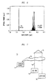
- FIG. 4 shows continuous wave (cw) light output vs. drive current, at various heat sink temperatures, for two deep-etched lasers of length 2.25 mm.
- the dashed lines were obtained from a laser with ternary top cladding, and the solid lines from a laser with InP top cladding.
- the lasers had cw power of about 200 mW/facet at 80K, at 8 ⁇ m wavelength. This output power is closely comparable to the 3 ⁇ m output power of the QC laser described in the above cited paper by Faist et al., IEEE J. Quantum Electronics , Vol. 34, p. 336 (1998).
- FIG. 5 shows peak output power vs. drive current, at various heat sink temperatures, for two shallow etched lasers of length 2.25 mm.
- the dashed lines were obtained from a laser with ternary top cladding, and the solid lines from a laser with InP top cladding.
- the lasers were operated in pulsed mode.
- FIG. 6 shows the normalized emission spectra of QC laser as described above (width 13 ⁇ m, length 2.25 mm), measured close to laser threshold cw and pulsed, respectively, at two different heat sink temperatures. The observed difference in the emission wavelengths reflects the temperature dependence of the gain spectrum of the lasers.
- the invention is described in detail in terms of a particular embodiment, having a 3-QW active region, with "vertical” laser transition.
- the lasing transition could be “diagonal”
- the active region could be a superlattice active region.
- QC lasers are advantageously used for, inter alia, detection and/or monitoring of trace gases, for example, for pollution monitoring, process control, medical or law-enforcement purposes, since these lasers can have output in one of the so-called atmospheric "windows", i.e., at a wavelength at which the clean atmosphere essentially does not absorb radiation.
- FIG. 7 schematically depicts an exemplary embodiment 70 of the invention, wherein an emission source 71 emits gas 72.
- QC laser 73 (advantageously a distributed feedback laser) emits mid-infrared radiation 74 that is directed through the emission gas, and is reflected, by any suitable means (e.g., corner reflector 75), to conventional detector 76.
- corner reflector 75 any suitable means
- the reflector could be replaced with a detector, such that the absorption during a single pass is measurable.
- the emission source is not necessarily a factory or other large-scale installation but could, for instance, be any source of a compound that has one or more absorption lines in the mid-IR.
- the source could, for instance, be a human subject, and the compound could be ethanol, or some medically significant compound.
- the gas sample could also be confined in a cell configured such that multi-path absorption is measured. For more detail on measurements, see EP-A-0877454.
Landscapes
- Physics & Mathematics (AREA)
- Optics & Photonics (AREA)
- Chemical & Material Sciences (AREA)
- Engineering & Computer Science (AREA)
- Nanotechnology (AREA)
- Condensed Matter Physics & Semiconductors (AREA)
- General Physics & Mathematics (AREA)
- Electromagnetism (AREA)
- Life Sciences & Earth Sciences (AREA)
- Biophysics (AREA)
- Crystallography & Structural Chemistry (AREA)
- Semiconductor Lasers (AREA)
Claims (7)
- Anordnung mit einem Quantenkaskadenlaser, welcher nacheinander eine obere optische Einschlusszone, eine Wellenleiter-Kernzone und eine untere optische Einschlusszone umfasst, und welcher ferner Kontakte zum elektrischen Kontaktieren des Lasers beinhaltet;dadurch gekennzeichnet, dass die Schichtstruktur vor allem so gewählt ist, dass sich bei einer anliegenden Vorspannung, die größer als die erste anliegende Vorspannung ist, sodass die Resonanz zwischen dem niedrigeren Energieniveau der ersten aktiven Zone und dem höheren Energieniveau der zweiten aktiven Zone zerstört wird, ein Grundzustand eines Minibandes in der Injektionszone auf im Wesentlichen derselben Energie befindet, wie das höhere Energieniveau der zweiten aktiven Zone, wodurch der Quantenkaskadenlaser einen breiten Aussteuerbereich des Stromes und zusammen damit eine hohe optische Leistung aufweist.wobei die Wellenleiter-Kernzone eine Vielzahl von im Wesentlichen identischen Wiederholungseinheiten umfasst, wobei eine gegebene Wiederholungseinheit eine Schichtstruktur aufweist, die eine Übergitter-Injektionszone beinhaltet, und eine aktive Zone, die so gewählt ist, dass sie einen strahlenden Elektronenübergang von einem höheren auf einen niedrigeren Energiezustand der aktiven Zone erleichtert; wobei die Injektionszone mehrere Quantentrogschichten umfasst, mit Barriereschichten, die zwischen die Quantentrogschichten geschichtet sind, wobei die Quantentrogschichten und die Barriereschichten so gewählt sind, dass sie bei einer geeigneten elektrischen Vorspannung einen Elektronenübergang von einem niedrigeren Energiezustand einer gegebenen aktiven Zone auf einen höheren Energiezustand einer unmittelbar stromab angrenzenden aktiven Zone erleichtern, wobei die gegebene Zone und die unmittelbar stromab angrenzende aktive Zone als die erste bzw. zweite aktive Zone bezeichnet werden sollen;wobei die Schichtstruktur so gewählt ist, dass sich bei einer ersten angelegten Vorspannung, die einer Lasingschwelle entspricht, ein niedrigeres Energieniveau (1) der ersten aktiven Zone auf im Wesentlichen derselben Energie wie ein höheres Energieniveau (3) der zweiten aktiven Zone befindet, und so, dass die Injektionszone zwischen der ersten und der zweiten aktiven Zone ohne wesentliche Relaxation der Elektronen in der Injektionszone einen hohen Elektronentransport durch die Injektionszone von dem niedrigeren Energieniveau der ersten aktiven Zone zu dem höheren Energieniveau der zweiten aktiven Zone erleichtert; und
- Anordnung nach Anspruch 1, bei welcher der strahlende Ladungsträgerübergang zur Emission eines Photons einer Wellenlänge im Wellenlängenbereich von 3 - 13 µm führt.
- Anordnung nach Anspruch 2, bei welcher die Wellenleiter-Kernzone zehn oder mehr Wiederholungseinheiten umfasst.
- Anordnung nach Anspruch 2, bei welcher die obere optische Einschlusszone InP umfasst.
- Anordnung nach Anspruch 2, bei welcher nur einige der Schichten der Injektionszone der gegebenen Wiederholungseinheit dotiert sind und der Rest der Schichten der Injektionszone nicht absichtlich dotiert sind.
- Anordnung nach Anspruch 1, bei welcher der Quantenkaskadenlaser eine Gitterstruktur beinhaltet.
- Anordnung nach Anspruch 1, wobei die Anordnung ein Messsystem ist, das dazu geeignet ist, die Absorption von Infrarotstrahlung durch ein Messobjekt zu messen, wobei das Messsystem einen Detektor beinhaltet, um Infrarotstrahlung von dem Laser nach Durchgang durch eine Anzahl von Messobjekten zu erfassen.
Applications Claiming Priority (2)
| Application Number | Priority Date | Filing Date | Title |
|---|---|---|---|
| US09/096,701 US6137817A (en) | 1998-06-12 | 1998-06-12 | Quantum cascade laser |
| US96701 | 1998-06-12 |
Publications (3)
| Publication Number | Publication Date |
|---|---|
| EP0964488A2 EP0964488A2 (de) | 1999-12-15 |
| EP0964488A3 EP0964488A3 (de) | 1999-12-22 |
| EP0964488B1 true EP0964488B1 (de) | 2001-11-07 |
Family
ID=22258659
Family Applications (1)
| Application Number | Title | Priority Date | Filing Date |
|---|---|---|---|
| EP99304076A Expired - Lifetime EP0964488B1 (de) | 1998-06-12 | 1999-05-26 | Verbesserter Quantumcascadelaser |
Country Status (4)
| Country | Link |
|---|---|
| US (1) | US6137817A (de) |
| EP (1) | EP0964488B1 (de) |
| JP (1) | JP3717712B2 (de) |
| DE (1) | DE69900427T2 (de) |
Families Citing this family (30)
| Publication number | Priority date | Publication date | Assignee | Title |
|---|---|---|---|---|
| WO2001026192A1 (en) * | 1999-10-07 | 2001-04-12 | Maxion Technologies, Inc. | Parallel cascade quantum well light emitting device |
| EP1130724A1 (de) * | 2000-03-03 | 2001-09-05 | Alpes Lasers | Quantenkaskadierter Laser und sein Herstellungsverfahren |
| DE10015615C2 (de) * | 2000-03-29 | 2002-07-11 | Draegerwerk Ag | Gasmesssystem |
| EP1195865A1 (de) * | 2000-08-31 | 2002-04-10 | Alpes Lasers SA | Quantenkaskadierter Laser |
| EP1189317A1 (de) * | 2000-09-13 | 2002-03-20 | Alpes Lasers SA | Quantenkaskadenlaser mit Anregung durch optische Phononen |
| DE10061234C2 (de) * | 2000-12-08 | 2003-01-16 | Paul Drude Inst Fuer Festkoerp | Unipolarer Halbleiterlaser ohne Injektionsschichten |
| US6690699B2 (en) * | 2001-03-02 | 2004-02-10 | Lucent Technologies Inc | Quantum cascade laser with relaxation-stabilized injection |
| US6795467B2 (en) | 2001-04-04 | 2004-09-21 | Lucent Technologies Inc. | Technique for measuring intersubband electroluminescence in a quantum cascade laser |
| EP1283571B1 (de) * | 2001-08-06 | 2015-01-14 | nanoplus GmbH Nanosystems and Technologies | Laser mit schwach gekoppeltem Gitterbereich |
| EP1343232B1 (de) * | 2002-03-08 | 2007-05-02 | nanoplus GmbH Nanosystems and Technologies | Ein Halbleiterlaserarray mit seitlicher Gratingstruktur |
| US6829269B2 (en) | 2002-05-21 | 2004-12-07 | University Of Massachusetts | Systems and methods using phonon mediated intersubband laser |
| US20040109692A1 (en) * | 2002-12-09 | 2004-06-10 | James Plante | FSO communication systems having high performance detectors |
| US20040161006A1 (en) * | 2003-02-18 | 2004-08-19 | Ying-Lan Chang | Method and apparatus for improving wavelength stability for InGaAsN devices |
| US7301977B2 (en) * | 2004-06-10 | 2007-11-27 | Nanoplus Gmbh | Tuneable unipolar lasers |
| CN100373724C (zh) * | 2005-08-31 | 2008-03-05 | 中国科学院上海微系统与信息技术研究所 | 磷化铟基含砷含磷量子级联激光器结构及不间断生长法 |
| JP5641667B2 (ja) * | 2007-01-18 | 2014-12-17 | 浜松ホトニクス株式会社 | 量子カスケードレーザ |
| DE102007002819B4 (de) * | 2007-01-19 | 2008-10-16 | Fraunhofer-Gesellschaft zur Förderung der angewandten Forschung e.V. | Unipolarer Quantenkaskaden-Laser hoher Effizienz |
| US20080273565A1 (en) * | 2007-05-04 | 2008-11-06 | Gmachl Claire F | Excited state quantum cascade photon source |
| US8014430B2 (en) * | 2008-02-27 | 2011-09-06 | President And Fellows Of Harvard College | Quantum cascade laser |
| FR2933542B1 (fr) * | 2008-07-04 | 2016-03-04 | Thales Sa | Dispositif a cascades quantiques a injecteur haut |
| US8351481B2 (en) * | 2008-11-07 | 2013-01-08 | President And Fellows Of Harvard College | Methods and apparatus for single-mode selection in quantum cascade lasers |
| JP2011035138A (ja) * | 2009-07-31 | 2011-02-17 | Hamamatsu Photonics Kk | 半導体発光素子 |
| JP5523759B2 (ja) * | 2009-07-31 | 2014-06-18 | 浜松ホトニクス株式会社 | 量子カスケードレーザ |
| DE102011117278B4 (de) | 2011-10-31 | 2014-07-10 | Julius-Maximilians-Universität Würzburg | Interbandkaskadenlaser-Verstärkermedium |
| US9608408B2 (en) | 2012-09-26 | 2017-03-28 | Pranalytica, Inc. | Long wavelength quantum cascade lasers based on high strain composition |
| US9088126B2 (en) | 2013-10-17 | 2015-07-21 | The Trustees Of Princeton University | Single-mode quantum cascade lasers with enhanced tuning range |
| EP3075040B1 (de) * | 2013-11-30 | 2018-08-08 | Thorlabs Quantum Electronics, Inc. | Quantenkaskadenlaser |
| JP6467193B2 (ja) * | 2014-10-30 | 2019-02-06 | 浜松ホトニクス株式会社 | 量子カスケードレーザ |
| JP2020123662A (ja) * | 2019-01-30 | 2020-08-13 | 住友電気工業株式会社 | 量子カスケードレーザ |
| WO2024105762A1 (ja) * | 2022-11-15 | 2024-05-23 | 三菱電機株式会社 | Qcl装置、外部共振型qclモジュール装置、分析装置及び光照射方法 |
Family Cites Families (5)
| Publication number | Priority date | Publication date | Assignee | Title |
|---|---|---|---|---|
| JPS63182550A (ja) * | 1987-01-23 | 1988-07-27 | Fujitsu Ltd | ガスセンサ |
| US5509025A (en) * | 1994-04-04 | 1996-04-16 | At&T Corp. | Unipolar semiconductor laser |
| US5457709A (en) * | 1994-04-04 | 1995-10-10 | At&T Ipm Corp. | Unipolar semiconductor laser |
| US5727010A (en) * | 1996-03-20 | 1998-03-10 | Lucent Technologies Inc. | Article comprising an improved quantum cascade laser |
| JP3159946B2 (ja) * | 1996-11-06 | 2001-04-23 | ルーセント テクノロジーズ インコーポレイテッド | 量子カスケードレーザを有する物品 |
-
1998
- 1998-06-12 US US09/096,701 patent/US6137817A/en not_active Expired - Lifetime
-
1999
- 1999-05-26 DE DE69900427T patent/DE69900427T2/de not_active Expired - Lifetime
- 1999-05-26 EP EP99304076A patent/EP0964488B1/de not_active Expired - Lifetime
- 1999-06-11 JP JP16456299A patent/JP3717712B2/ja not_active Expired - Lifetime
Also Published As
| Publication number | Publication date |
|---|---|
| JP2000012983A (ja) | 2000-01-14 |
| DE69900427T2 (de) | 2002-06-27 |
| EP0964488A3 (de) | 1999-12-22 |
| JP3717712B2 (ja) | 2005-11-16 |
| US6137817A (en) | 2000-10-24 |
| DE69900427D1 (de) | 2001-12-13 |
| EP0964488A2 (de) | 1999-12-15 |
Similar Documents
| Publication | Publication Date | Title |
|---|---|---|
| EP0964488B1 (de) | Verbesserter Quantumcascadelaser | |
| Sirtori et al. | GaAs/Al x Ga 1− x As quantum cascade lasers | |
| Gmachl et al. | High-power λ≈ 8 μ m quantum cascade lasers with near optimum performance | |
| US6501783B1 (en) | Distributed feedback surface plasmon laser | |
| US7856042B2 (en) | High efficiency intersubband semiconductor lasers | |
| US5936989A (en) | Quantum cascade laser | |
| EP0867990B1 (de) | Gegenstand der einen mit einem elektrischen Feld abstimmbaren Halbleiterlaser enthält | |
| US20060039431A1 (en) | Quantum cascade laser device | |
| US6301282B1 (en) | Long wavelength semiconductor lasers incorporating waveguides based on surface plasmons | |
| US6148012A (en) | Multiple wavelength quantum cascade light source | |
| EP0797280B1 (de) | Gegenstand bestehend aus einem verbesserter Quantumcasadelaser | |
| EP1215781B1 (de) | Intersubband Übergitter lichtemittierende Vorrichtung | |
| EP1500176B1 (de) | Thz-halbleiterlaser mit einem gesteuerten plasmon-confinement-wellenleiter | |
| Yang et al. | Improvement of λ≈ 5 μ m quantum cascade lasers by blocking barriers in the active regions | |
| Gmachl et al. | Noncascaded intersubband injection lasers at λ≈ 7.7 μ m | |
| EP0841731B1 (de) | Quantum Cascade Laser | |
| EP0932230B1 (de) | Vorrichtung mit einem spannungskompensierter QC Laser | |
| Gmachl et al. | Long wavelength (λ≃ 13 µm) quantum cascade lasers | |
| EP0957547B1 (de) | Gegenstand bestehend aus einem verbesserten Übergitterquantumcascadelaser | |
| Friedrich et al. | High performance injectorless quantum-cascade lasers | |
| Tredicucci et al. | Terahertz quantum cascade lasers | |
| EP3893341B1 (de) | Quantenkaskadenlaserelement | |
| Gianordoli et al. | Improved performance of GaAs-AlGaAs superlattice quantum cascade lasers beyond/spl lambda/= 13 μm | |
| Strasser et al. | Intersubband and interminiband GaAs/AlGaAs quantum cascade lasers | |
| Tredicucci et al. | Superlattice quantum cascade lasers |
Legal Events
| Date | Code | Title | Description |
|---|---|---|---|
| PUAI | Public reference made under article 153(3) epc to a published international application that has entered the european phase |
Free format text: ORIGINAL CODE: 0009012 |
|
| PUAL | Search report despatched |
Free format text: ORIGINAL CODE: 0009013 |
|
| 17P | Request for examination filed |
Effective date: 19990607 |
|
| AK | Designated contracting states |
Kind code of ref document: A2 Designated state(s): DE FR GB |
|
| AX | Request for extension of the european patent |
Free format text: AL;LT;LV;MK;RO;SI |
|
| AK | Designated contracting states |
Kind code of ref document: A3 Designated state(s): AT BE CH CY DE DK ES FI FR GB GR IE IT LI LU MC NL PT SE |
|
| AX | Request for extension of the european patent |
Free format text: AL;LT;LV;MK;RO;SI |
|
| 17Q | First examination report despatched |
Effective date: 20000322 |
|
| AKX | Designation fees paid | ||
| REG | Reference to a national code |
Ref country code: DE Ref legal event code: 8566 |
|
| RBV | Designated contracting states (corrected) |
Designated state(s): DE FR GB |
|
| GRAG | Despatch of communication of intention to grant |
Free format text: ORIGINAL CODE: EPIDOS AGRA |
|
| RIC1 | Information provided on ipc code assigned before grant |
Free format text: 7H 01S 5/34 A |
|
| GRAG | Despatch of communication of intention to grant |
Free format text: ORIGINAL CODE: EPIDOS AGRA |
|
| GRAH | Despatch of communication of intention to grant a patent |
Free format text: ORIGINAL CODE: EPIDOS IGRA |
|
| GRAH | Despatch of communication of intention to grant a patent |
Free format text: ORIGINAL CODE: EPIDOS IGRA |
|
| GRAA | (expected) grant |
Free format text: ORIGINAL CODE: 0009210 |
|
| RIN1 | Information on inventor provided before grant (corrected) |
Inventor name: TREDICUCCI, ALESSANDRO Inventor name: SIVCO, DEBORAH LEE Inventor name: HUTCHINSON, ALBERT LEE Inventor name: GMACHL, CLAIRE F. Inventor name: CHO, ALFRED YI Inventor name: CAPASSO, FEDERICO Inventor name: BAILLARGEON, JAMES NELSON |
|
| AK | Designated contracting states |
Kind code of ref document: B1 Designated state(s): DE FR GB |
|
| REG | Reference to a national code |
Ref country code: DE Ref legal event code: 8570 |
|
| REF | Corresponds to: |
Ref document number: 69900427 Country of ref document: DE Date of ref document: 20011213 |
|
| REG | Reference to a national code |
Ref country code: GB Ref legal event code: IF02 |
|
| PLBE | No opposition filed within time limit |
Free format text: ORIGINAL CODE: 0009261 |
|
| STAA | Information on the status of an ep patent application or granted ep patent |
Free format text: STATUS: NO OPPOSITION FILED WITHIN TIME LIMIT |
|
| 26N | No opposition filed | ||
| REG | Reference to a national code |
Ref country code: GB Ref legal event code: 732E Free format text: REGISTERED BETWEEN 20131031 AND 20131106 |
|
| REG | Reference to a national code |
Ref country code: FR Ref legal event code: CD Owner name: ALCATEL-LUCENT USA INC. Effective date: 20131122 |
|
| REG | Reference to a national code |
Ref country code: FR Ref legal event code: GC Effective date: 20140410 |
|
| REG | Reference to a national code |
Ref country code: FR Ref legal event code: RG Effective date: 20141015 |
|
| REG | Reference to a national code |
Ref country code: FR Ref legal event code: PLFP Year of fee payment: 17 |
|
| PGFP | Annual fee paid to national office [announced via postgrant information from national office to epo] |
Ref country code: GB Payment date: 20150521 Year of fee payment: 17 Ref country code: DE Payment date: 20150521 Year of fee payment: 17 |
|
| PGFP | Annual fee paid to national office [announced via postgrant information from national office to epo] |
Ref country code: FR Payment date: 20150521 Year of fee payment: 17 |
|
| REG | Reference to a national code |
Ref country code: DE Ref legal event code: R119 Ref document number: 69900427 Country of ref document: DE |
|
| GBPC | Gb: european patent ceased through non-payment of renewal fee |
Effective date: 20160526 |
|
| REG | Reference to a national code |
Ref country code: FR Ref legal event code: ST Effective date: 20170131 |
|
| PG25 | Lapsed in a contracting state [announced via postgrant information from national office to epo] |
Ref country code: FR Free format text: LAPSE BECAUSE OF NON-PAYMENT OF DUE FEES Effective date: 20160531 Ref country code: DE Free format text: LAPSE BECAUSE OF NON-PAYMENT OF DUE FEES Effective date: 20161201 |
|
| PG25 | Lapsed in a contracting state [announced via postgrant information from national office to epo] |
Ref country code: GB Free format text: LAPSE BECAUSE OF NON-PAYMENT OF DUE FEES Effective date: 20160526 |