EP0959423B1 - Connecteur pour carte - Google Patents
Connecteur pour carte Download PDFInfo
- Publication number
- EP0959423B1 EP0959423B1 EP99302865A EP99302865A EP0959423B1 EP 0959423 B1 EP0959423 B1 EP 0959423B1 EP 99302865 A EP99302865 A EP 99302865A EP 99302865 A EP99302865 A EP 99302865A EP 0959423 B1 EP0959423 B1 EP 0959423B1
- Authority
- EP
- European Patent Office
- Prior art keywords
- cover
- card
- lock
- lock bar
- portions
- Prior art date
- Legal status (The legal status is an assumption and is not a legal conclusion. Google has not performed a legal analysis and makes no representation as to the accuracy of the status listed.)
- Expired - Lifetime
Links
Images


Classifications
-
- H—ELECTRICITY
- H01—ELECTRIC ELEMENTS
- H01R—ELECTRICALLY-CONDUCTIVE CONNECTIONS; STRUCTURAL ASSOCIATIONS OF A PLURALITY OF MUTUALLY-INSULATED ELECTRICAL CONNECTING ELEMENTS; COUPLING DEVICES; CURRENT COLLECTORS
- H01R13/00—Details of coupling devices of the kinds covered by groups H01R12/70 or H01R24/00 - H01R33/00
- H01R13/02—Contact members
- H01R13/22—Contacts for co-operating by abutting
- H01R13/24—Contacts for co-operating by abutting resilient; resiliently-mounted
- H01R13/2442—Contacts for co-operating by abutting resilient; resiliently-mounted with a single cantilevered beam
-
- G—PHYSICS
- G06—COMPUTING; CALCULATING OR COUNTING
- G06K—GRAPHICAL DATA READING; PRESENTATION OF DATA; RECORD CARRIERS; HANDLING RECORD CARRIERS
- G06K13/00—Conveying record carriers from one station to another, e.g. from stack to punching mechanism
- G06K13/02—Conveying record carriers from one station to another, e.g. from stack to punching mechanism the record carrier having longitudinal dimension comparable with transverse dimension, e.g. punched card
- G06K13/08—Feeding or discharging cards
- G06K13/085—Feeding or discharging cards using an arrangement for locking the inserted card
-
- G—PHYSICS
- G06—COMPUTING; CALCULATING OR COUNTING
- G06K—GRAPHICAL DATA READING; PRESENTATION OF DATA; RECORD CARRIERS; HANDLING RECORD CARRIERS
- G06K7/00—Methods or arrangements for sensing record carriers, e.g. for reading patterns
- G06K7/0013—Methods or arrangements for sensing record carriers, e.g. for reading patterns by galvanic contacts, e.g. card connectors for ISO-7816 compliant smart cards or memory cards, e.g. SD card readers
- G06K7/0021—Methods or arrangements for sensing record carriers, e.g. for reading patterns by galvanic contacts, e.g. card connectors for ISO-7816 compliant smart cards or memory cards, e.g. SD card readers for reading/sensing record carriers having surface contacts
-
- H—ELECTRICITY
- H01—ELECTRIC ELEMENTS
- H01R—ELECTRICALLY-CONDUCTIVE CONNECTIONS; STRUCTURAL ASSOCIATIONS OF A PLURALITY OF MUTUALLY-INSULATED ELECTRICAL CONNECTING ELEMENTS; COUPLING DEVICES; CURRENT COLLECTORS
- H01R13/00—Details of coupling devices of the kinds covered by groups H01R12/70 or H01R24/00 - H01R33/00
- H01R13/62—Means for facilitating engagement or disengagement of coupling parts or for holding them in engagement
- H01R13/627—Snap or like fastening
-
- Y—GENERAL TAGGING OF NEW TECHNOLOGICAL DEVELOPMENTS; GENERAL TAGGING OF CROSS-SECTIONAL TECHNOLOGIES SPANNING OVER SEVERAL SECTIONS OF THE IPC; TECHNICAL SUBJECTS COVERED BY FORMER USPC CROSS-REFERENCE ART COLLECTIONS [XRACs] AND DIGESTS
- Y10—TECHNICAL SUBJECTS COVERED BY FORMER USPC
- Y10S—TECHNICAL SUBJECTS COVERED BY FORMER USPC CROSS-REFERENCE ART COLLECTIONS [XRACs] AND DIGESTS
- Y10S439/00—Electrical connectors
- Y10S439/91—Observation aide, e.g. transparent material, window in housing
Definitions
- This invention relates to a connector for an integrated circuit (IC) card which is, in use, attached to a given electronic device such as a telephone set, a cash dispenser, a personal computer, a camera, or the like.
- IC integrated circuit
- a card connector as discussed in Japanese Patent Publication (Kokai) No. Hei 9-185973 and corresponding US patent 5,813,878 , which comprises a connector housing constituted by a base and a cover openable and closable with respect to the base, the base being provided with a plurality of contacts arranged thereon in such a manner as to be able to contact external terminals of an IC card received in the connector housing, and a lock mechanism for maintaining a closed position of the cover with respect to the base.
- a lock pawl is raised from a side plate of the cover and this lock pawl, when the cover is closed with respect to the base, is snap fitted into a lock hole for a resilient lock piece provided on the base.
- a known card connector is discussed in US 5337220 , which comprises a base member and a hollow casing pivotably mounted on the base member.
- a casing of a card reader uses both rotatable means and hooks to adjust the casing properly.
- a docking assembly is disclosed for mechanically interfacing a modular component with a circuit board to complete and protect multiple electrical connections there between.
- the present invention has been accomplished in view of the above shortcomings inherent in the conventional devices.
- Another object of the present invention is to provide a card connector capable of providing a reliable connection between contacts thereof and terminals of an IC card.
- a further object of the present invention is to provide a card connector in which a soldering state of a surface mounting terminal can be visually recognized.
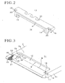
- a card connector of the present invention includes a base 1 made of insulative material and a cover 2 made of insulative material or metal material.
- the cover 2 is attached at its basal end to a basal end of the base 1 through a pin 3 such that the cover 2 can rotate about the pin 3. Rotation of the cover 2 makes it possible to close the cover 2 with respect to the base 1.
- the base 1 and the cover 2 constitute a flat and square connector housing for receiving an IC card 4.
- the base 1 forming the connector housing has a plurality of contacts 5.
- the contacts 5 are each formed of an electrically conductive elongate piece which is punched out of a metal plate and bent.
- the contacts 5 are arranged in array in such a manner as to correspond to external terminals 8 of the IC card 4. In this embodiment, a group of the contacts 5 are arranged in two rows as shown in Fig. 4.
- a contact portion 7 projecting from an inner surface (upper surface) of the base 1 is formed on a free end of the electrically conductive elongate piece which constitutes each contact 5.
- the electrically conductive elongate piece constituting each contact 5 has a resilient contact piece 6 extending in a direction of insertion of the IC card 4 from an implanting portion of thereof.
- the contact portion 7 is formed on a free end of the resilient contact piece 6.
- the electrically conductive elongate piece also has a surface mount terminal 11 projecting in the other side of the resilient contact piece 6. Through this surface mount terminal 11, the contact 5 is connected to a circuit board 12 in a given electronic device by soldering or the like.
- the IC card 4 exhibits a flat and generally square configuration.
- the IC card 4 has an IC chip for recording or reading data stored in the IC card 4.
- External contacts 8 of the IC chip are arranged in array on a front surface of the IC card 4 in such a manner as to correspond to the contact portions 7 of the contacts 5.
- the IC card 4 is connected to a data processing circuit in a given electronic device such as a telephone set or the like through the card connector, so that data stored in the IC card 4 are given to the electronic device or data stored in the electronic device are taken into the IC card 4.
- the IC card 4 is inserted into a cover 2.
- the cover 2 has a card receiving space 9 disposed along an inner surface (under surface) of a top plate 2a.
- the card receiving space 9 is opened at a free end of the cover 2.
- the free end of the cover 2 is located on the other side of a basal end of the cover 2 where the cover 2 is supported through a pin.
- the opening of the card receiving space 9, which is opened at the free end of the cover 2 is defined as a card receiving port 10.
- the IC card 4 is inserted into and withdrawn from the card receiving space 9 through the card receiving port 10.
- One pair of left and right guide rails 2b, 2b extend from the basal end of the cover 2 to a free end thereof along opposite left and right sides of the top plate 2a of the cover 2.
- the one pair of left and right guie rails 2b, 2b are integral with the top plate 2a of the cover 2.
- the card receiving space 9 is defined by the one pair of left and right guide rails 2b, 2b and the top plate 2a.
- the card receiving space 9 is opened at a free end of the top plate 2a and at free ends of the one pair of left and right guide rails 2b, 2b, thereby forming the card receiving port 10.
- Left and right side walls 2c, 2c are formed on left and right sides of the top plate 2a in such a manner as to be integral with the top plate 2a.
- One pair of left and right bottom walls 2d, 2d extend inwardly from the one pair of left and right side walls 2c, 2c.
- the one pair of left and right guide rails 2b, 2b having one pair of left and right guide grooves 2e, 2e are defined by the one pair of left and right bottom walls 2d, 2d, the one pair of left and right side walls 2c, 2c and the top plate 2a.
- the one pair of left and right side walls 2c, 2c form a side scale for restricting left and right side surfaces of the IC card 4,
- the one pair of left and right bottom wall 2d, 2d form a bottom scale for restricting under surfaces of left and right side edge portions of the IC card 4,
- an inner surface (under surface) of the left and right side edge portions of the top plate 2a form a top scale for restricting upper surfaces of the left and right side edge portions of the IC card 4.
- the one pair of left and right side walls 2c, 2c and the one pair of left and right bottom walls 2d, 2d extend from the basal end of the top plate 2a to the free end along the left and right side edges of the top plate 2a, thereby forming the one pair of left and right guide rails 2b, 2b.
- the cover 2 is rotated about the pin 3 so as to be closed with respect to the base 1, so that each external terminal 8 of the IC card 4 is pushed against the contact portion 7 of the corresponding contact 5.
- the resilient contact piece 6 of the contact 5 is displaced against resiliency thereof, and the contact portion 7 is brought into contact, under pressure, with the external terminal 8 by reaction thereof.
- the cover 2 which is formed of an electrical conductive metal plate, covers the IC card 4.
- the electrically conductive cover 2 when closed with respect to the base 1, is connected to an earth line of a circuit board 12 through a shielding contact element provided on the base 1, thus enabling to form a shield structure on a local portion of the cover 2.
- a lock mechanism for holding a closed position of the cover 2 with respect to the base 1.
- a pressure contacted relation between the contact 5 of the card connector and the external terminal 8 of the IC card 4 is maintained by holding the closed position of the cover 2 with respect to the base 1 by the lock mechanism.
- a lock bar 13 extending in parallel to the card receiving port 10 is supported by pin holes 14' through pins 14 on the other end portion of the base 1 such that the lock bar 13 can be rotated in a locking direction and in an unlocking direction and then resiliently held in the locking direction by a spring 15.
- the spring 15 for resiliently holding the lock bar 13 is formed of an elongate plate spring.
- a basal end of this plate spring 15 is fixed to one end portion of the base 1 by insert molding or the like and allowed to project downwardly of the lock bar 13 from the end edge of the base 1.
- a free end of the spring 15 resiliently contacts an under surface of the lock bar 13, thereby normally resiliently holding the lock bar 13 in the locking direction.
- One pair of lock portions 16 are provided on longitudinal opposite ends (left and right ends) of the lock bar 13.
- the guide rails 2b, 2b are provided on free ends thereof with one pair of opponent portions 17.
- each guide rail 2b is allowed to project in its extending direction, and the opponent portion 17 is formed on a projecting portion of the guide rail 2b.
- An upper surface of the opponent portion 17 is stepped 18 such that the stepped area 18 of the upper surface of the opponent portion 17 is lower than the upper surface of the top plate 2a.
- the lock portion 16 of the lock bar 13 is hooked on the stepped area of the opponent portion 17, thereby retaining the closed position of the cover 2 with respect to the cover 2.
- the lock portion 16 of the lock bar 13 is provided with a first guide surface 20.
- This first guide surface 20 when the cover 2 is closed with respect to the base 1, is pushed by the opponent portion 17 of the cover 2 to rotate the lock bar 13 slightly in the unlocking direction against the resiliency.
- the lock bar 13 is formed on an inner surface thereof with a second guide surface 21.
- This second guide surface 21 is slanted to guide the end edge of the IC card in accordance with the rotation of the lock bar 13.
- the lock portion 16 is provided on a free end portion of the lock bar 13 and has a hook-like configuration in section.
- a slanted surface comprised of a curved or straight surface facing with the card receiving port 10 is formed in such a manner as to be continuous with a top surface of the hook portion. This slanted surface is served as the first guide surface 20.
- the lock bar 13 has an inner surface continuous with a top surface thereof or a top surface of that portion of the lock bar 13 which extends between the one pair of lock portions 16 and faced with the card receiving port 10.
- This inner surface is slanted as the lock bar 13 is rotated slightly in the unlocking direction through coaction between the opponent portion 17 and the first guide surface 20.
- This slanted inner surface is served as the second guide surface 21.
- the contacts on one row each have a surface mount terminal 11 projecting downwardly of the lock bar 13.
- the lock bar 13 is provided with an opening portion 22 through which the surface mount terminal 11 can be visually vertically recognized.
- cutout portions corresponding the the surface mount terminals 11 are formed along the end edge of the lock bar 13. Those cutout portions are served as the opening portions 22.
- the surface mount terminals 11 of the contacts 5 arranged on the other row are located on the side where the cover 2 is supported on the base 1 through the pin, so that the surface mount terminals 11 can be visually vertically recognized through the window 23 formed on the top plate 2a of the cover 2.
- the return spring is formed of, for example, an elongate plate spring 24.
- One end of the plate spring 24 is insert-molded to the vicinity of the area where the cover 2 is supported on the base 1 through the pin and the other end is allowed to extend towards the free end side of the cover 2 so as to be resiliently contacted with the under surface of the guide rail 2b, i.e., the under surface of the bottom wall 2d forming the guide rail 2b, thereby pushing up the overall cover 2.
- one pair of the right and left springs 24 are arranged in such a manner as to push up the one pair of guide rails 2b.
- the cover 2 is closed against the effects of both the spring 24 and the contacts 5 and opened by the restoring forces of spring 24 and contacts 5.
- the present invention relates to a card connector, in which an IC card is retained by the cover and the cover with the IC card is closed with respect to the base so that the external terminals of the IC card are brought into contact, under pressure, with the contacts arranged on the base.
- this card connector it is indispensable to provide a lock mechanism for maintaining the pressure contact state between the card and the contacts by maintaining the closed position of the cover with respect to the base.
- the lock bar which is rotatably supported, through a pin, on an end portion of the base in its lateral posture and resiliently held in the locking direction, is detachably attached to a free end of the cover. Owing to this arrangement, the cover can be opened and closed easily and reliably.
- the connector can be made small in size and thin in design.
- the IC card inserted into the cover can easily visually be recognized through the window formed between the free end edges of the lock bar and the top plate of the cover. This enhances a smooth insertion and withdrawal of the IC card with ease.
- the cover retaining the IC card can easily be brought into a closed position and the IC card can efficiently be guided to the position where the IC card is brought into electrical connection with the contacts.
Landscapes
- Engineering & Computer Science (AREA)
- Physics & Mathematics (AREA)
- General Physics & Mathematics (AREA)
- Theoretical Computer Science (AREA)
- Artificial Intelligence (AREA)
- Computer Vision & Pattern Recognition (AREA)
- Coupling Device And Connection With Printed Circuit (AREA)
- Details Of Connecting Devices For Male And Female Coupling (AREA)
Claims (8)
- Connecteur de carte comprenant :une base (1) avec une extrémité basale et une deuxième extrémité ;un couvercle (2) qui est soutenu de façon pivotante sur ladite extrémité basale de ladite base par une broche (3) de sorte que le couvercle (2) puisse pivoter entre une position ouverte et une position fermée par rapport à ladite base (1) ;ledit couvercle (2) incluant une plaque supérieure ainsi qu'un premier et un deuxième rails de guidage (2b) qui se prolongent à partir d'une extrémité basale dudit couvercle vers une extrémité libre dudit couvercle (2) le long du premier et du deuxième côtés de ladite plaque supérieure, un espace de réception de carte (9) étant défini dans ledit couvercle par ladite plaque supérieure ainsi que par lesdits premier et deuxième rails de guidage, ledit espace de réception de carte s'ouvrant au niveau de ladite extrémité libre dudit couvercle afin de définir un port de réception de carte (10) qui s'étend à partir dudit premier rail de guidage vers ledit deuxième rail de guidage ;une pluralité de contacts qui sont agencés sur ladite base pour assurer un contact sous pression avec des bornes externes (8) d'une carte à circuits intégrés (4) lorsque la carte à circuits intégrés (4) est introduite dans ledit espace de réception de carte (9) et que ledit couvercle (2) se trouve dans ladite position fermée ;une barre de verrouillage allongée (13) laquelle s'étend en parallèle par rapport audit port de réception de carte (10) ;dans lequel lesdits premier et deuxième rails de guidage (2b) sont munis, sur ceux-ci, de sections d'engagement de verrou (17), respectivement, au niveau de ladite extrémité libre dudit couvercle ;dans lequel ladite barre de verrouillage allongée (13) est munie, au niveau des extrémités opposées de celle-ci, de sections de verrouillage (16) qui sont aptes à être engagées avec lesdites sections d'engagement de verrou (17) desdits premier et deuxième rails de guidage (2b), respectivement ;dans lequel chacune desdites sections de verrouillage (16) de ladite barre de verrouillage allongée (13) est pourvue d'une première surface de guidage (20),et caractérisé en ce que ladite barre de verrouillage allongée (13) est montée de façon rotative au niveau de ladite deuxième extrémité de ladite base (1) pour pouvoir effectuer une rotation dans une direction de verrouillage vers l'engagement desdites sections de verrouillage (16) de ladite barre de verrouillage avec lesdites sections d'engagement de verrou (17) desdits premier et deuxième rails de guidage (2b), ainsi que dans une direction de déverrouillage qui est opposée à ladite direction de verrouillage ;dans lequel ladite barre de verrouillage allongée (13) est poussée de façon élastique afin de tourner dans ladite direction de verrouillage ; etdans lequel lesdites premières surfaces de guidage (20) sont agencées de sorte que, lors du pivotement dudit couvercle (12) vers ladite position fermée, lesdites premières surfaces de guidage (20) sont poussées par lesdites sections d'engagement de verrou (17), respectivement, afin de faire tourner ladite barre deverrouillage allongée (13) dans ladite direction de déverrouillage.
- Connecteur de carte, selon la revendication 1, dans lequel
ladite barre de verrouillage allongée (13) est pourvue, au niveau de la face intérieure desdites sections de verrouillage (16), d'une deuxième surface de guidage (21) pour guider un bord d'extrémité de la carte à circuits intégrés (4) lorsque la carte à circuits intégrés est reçue dans ledit espace de réception de carte (9) et lors du pivotement dudit couvercle vers ladite position fermée. - Connecteur de carte, selon la revendication 1, dans lequel
chacun desdits contacts comporte une borne pour montage en surface qui se projette sous ladite barre de verrouillage allongée (13), et
ladite barre de verrouillage allongée possède une ouverture à travers laquelle il est possible de voir, à partir du haut, lesdites bornes pour montage en surface desdits contacts. - Connecteur de carte, selon la revendication 1, dans lequel
lesdits premier et deuxième rails de guidage (2b) comportent des sections se projetant vers l'avant qui s'étendent au-delà de ladite plaque supérieure (2a) dans une direction partant de ladite extrémité basale dudit couvercle vers ladite extrémité libre de celui-ci, et
lesdites sections se projetant vers l'avant comprennent lesdites sections d'engagement de verrou
desdits premier et deuxième rails de guidage, respectivement. - Connecteur de carte, selon la revendication 4, dans lequel
lesdites sections d'engagement de verrou desdits premier et deuxième rails de guidage comportent des zones en gradin descendantes en surface supérieure desdites sections se projetant vers l'avant desdits premier et deuxième rails de guidage, respectivement, et lesdites zones en gradin peuvent être engagées dans lesdites sections de verrouillage de ladite barre de verrouillage allongée (13), respectivement. - Connecteur de carte, selon la revendication 5, dans lequel
ladite barre de verrouillage allongée (13) est pourvue, au niveau de la face intérieure desdites sections de verrouillage, d'une deuxième surface de guidage pour guider un bord d'extrémité de la carte à circuits intégrés lorsque la carte à circuits intégrés (4) est reçue dans ledit espace de réception de carte (9) et lors du pivotement dudit couvercle vers ladite position fermée. - Connecteur de carte, selon la revendication 5, dans lequel
chacun desdits contacts comporte une borne pour montage en surface qui se projette sous ladite barre de verrouillage allongée (13) ; et
ladite barre de verrouillage allongée possède une ouverture à travers laquelle il est possible de voir, à partir du haut, lesdites bornes pour montage en surface desdits contacts. - Connecteur de carte, selon la revendication 1, dans lequel
lesdits premier et deuxième rails de guidage possèdent (2b) une première et une deuxième parois inférieures qui sont prévues sur ceux-ci et qui s'étendent le long de ceux-ci afin de soutenir la carte à circuits intégrés (4).
Applications Claiming Priority (2)
| Application Number | Priority Date | Filing Date | Title |
|---|---|---|---|
| JP13577298 | 1998-05-18 | ||
| JP10135772A JP2957554B1 (ja) | 1998-05-18 | 1998-05-18 | カードコネクタ |
Publications (3)
| Publication Number | Publication Date |
|---|---|
| EP0959423A2 EP0959423A2 (fr) | 1999-11-24 |
| EP0959423A3 EP0959423A3 (fr) | 1999-12-08 |
| EP0959423B1 true EP0959423B1 (fr) | 2007-08-29 |
Family
ID=15159506
Family Applications (1)
| Application Number | Title | Priority Date | Filing Date |
|---|---|---|---|
| EP99302865A Expired - Lifetime EP0959423B1 (fr) | 1998-05-18 | 1999-04-13 | Connecteur pour carte |
Country Status (4)
| Country | Link |
|---|---|
| US (1) | US6227893B1 (fr) |
| EP (1) | EP0959423B1 (fr) |
| JP (1) | JP2957554B1 (fr) |
| DE (1) | DE69936956D1 (fr) |
Families Citing this family (22)
| Publication number | Priority date | Publication date | Assignee | Title |
|---|---|---|---|---|
| US6493033B1 (en) * | 1998-12-09 | 2002-12-10 | Eastman Kodak Company | Electronic apparatus adapted to receive a memory card |
| FR2796763B1 (fr) * | 1999-07-23 | 2002-02-01 | Itt Mfg Enterprises Inc | Connecteur electrique pour carte a circuit(s) integre(s) comportant un commutateur de verrou du couvercle porte carte |
| FR2805401A1 (fr) * | 2000-02-18 | 2001-08-24 | Itt Mfg Enterprises Inc | Connecteur electrique ergonomique pour carte a circuit(s) integre(s) |
| TW474466U (en) * | 2000-06-03 | 2002-01-21 | Hon Hai Prec Ind Co Ltd | Electronic card connector |
| JP4671484B2 (ja) * | 2000-10-11 | 2011-04-20 | ケル株式会社 | カードコネクタ |
| JP4297633B2 (ja) * | 2001-07-12 | 2009-07-15 | アルプス電気株式会社 | カード用コネクタ装置 |
| JP2003178846A (ja) * | 2001-12-12 | 2003-06-27 | Tyco Electronics Amp Kk | カードコネクタ |
| WO2003054776A1 (fr) * | 2001-12-21 | 2003-07-03 | Nokia Corporation | Dispositif de lecture d'une carte sim ultra mince destine a un dispositif de communication, notamment un telephone mobile |
| US6865086B2 (en) * | 2002-07-09 | 2005-03-08 | Micron Technology, Inc. | Apparatus and method to secure an adaptor to a reduced-sized memory card |
| US7344296B2 (en) | 2003-02-07 | 2008-03-18 | Matsushita Electric Industrial Co., Ltd. | Socket for led light source and lighting system using the socket |
| TW588869U (en) * | 2003-04-02 | 2004-05-21 | High Tech Comp Corp | A card connector with reinforce structure |
| TWM240699U (en) * | 2003-08-29 | 2004-08-11 | Molex Taiwan Ltd | Card edge connector assembly |
| TWM253105U (en) * | 2003-11-04 | 2004-12-11 | Hon Hai Prec Ind Co Ltd | Electrical card connector |
| KR20060097979A (ko) * | 2005-03-08 | 2006-09-18 | 주식회사 매커스 | 탑 로딩식 카드 어댑터 |
| JP5004443B2 (ja) * | 2005-07-19 | 2012-08-22 | モレックス インコーポレイテド | ヒンジ式カバーを備えたメモリカードコネクタ |
| CN101083362A (zh) * | 2006-05-31 | 2007-12-05 | 富士康(昆山)电脑接插件有限公司 | 扣持装置及具有该装置的卡缘连接器 |
| TWM311153U (en) * | 2006-08-16 | 2007-05-01 | Advanced Connectek Inc | Electric connector |
| TWI429149B (zh) * | 2011-05-10 | 2014-03-01 | Wistron Corp | 用來連接板卡之連接器機構 |
| CN105449433B (zh) * | 2015-06-01 | 2018-03-06 | 富士康(昆山)电脑接插件有限公司 | 电连接器及其制造方法 |
| JP7312531B2 (ja) * | 2018-05-28 | 2023-07-21 | イリソ電子工業株式会社 | 撮像装置及び可動コネクタと外部接続ケースとの接続構造 |
| CN111064045A (zh) * | 2019-12-23 | 2020-04-24 | 北京空天技术研究所 | 脱落插座的防护结构 |
| JP6901602B1 (ja) * | 2020-03-27 | 2021-07-14 | 日本航空電子工業株式会社 | コネクタ |
Citations (3)
| Publication number | Priority date | Publication date | Assignee | Title |
|---|---|---|---|---|
| US5211566A (en) * | 1992-08-11 | 1993-05-18 | Amp Incorporated | Docking connector for disk drives |
| US5813878A (en) * | 1995-12-28 | 1998-09-29 | Hirose Electric Co., Ltd. | Surface contact card connector |
| US5933328A (en) * | 1998-07-28 | 1999-08-03 | Sandisk Corporation | Compact mechanism for removable insertion of multiple integrated circuit cards into portable and other electronic devices |
Family Cites Families (8)
| Publication number | Priority date | Publication date | Assignee | Title |
|---|---|---|---|---|
| DE3518247A1 (de) * | 1985-05-21 | 1986-11-27 | Siemens AG, 1000 Berlin und 8000 München | Ver- und entriegelungseinrichtung fuer einen kartenleser |
| JPS62219193A (ja) | 1986-03-20 | 1987-09-26 | Oki Electric Ind Co Ltd | Icカ−ド・リ−ダライタ |
| GB2250846B (en) | 1990-12-13 | 1994-08-24 | Technophone Ltd | Card reader |
| FR2676566B1 (fr) | 1991-05-13 | 1993-12-17 | Alcatel Cit | Connecteur pour carte a circuits. |
| JP3397345B2 (ja) | 1992-08-31 | 2003-04-14 | キヤノン株式会社 | 記録媒体のローディング機構 |
| US5337220A (en) | 1993-09-10 | 1994-08-09 | The Whitaker Corporation | Electronic card and connector assembly for use therewith |
| JP3236753B2 (ja) * | 1995-03-03 | 2001-12-10 | ホシデン株式会社 | カードコネクタにおけるカード保持装置 |
| EP0840246B2 (fr) | 1996-11-05 | 2011-03-16 | Amphenol-Tuchel Electronics GmbH | Dispositif de contact pour cartes SIM |
-
1998
- 1998-05-18 JP JP10135772A patent/JP2957554B1/ja not_active Expired - Fee Related
-
1999
- 1999-04-12 US US09/289,632 patent/US6227893B1/en not_active Expired - Fee Related
- 1999-04-13 EP EP99302865A patent/EP0959423B1/fr not_active Expired - Lifetime
- 1999-04-13 DE DE69936956T patent/DE69936956D1/de not_active Expired - Lifetime
Patent Citations (3)
| Publication number | Priority date | Publication date | Assignee | Title |
|---|---|---|---|---|
| US5211566A (en) * | 1992-08-11 | 1993-05-18 | Amp Incorporated | Docking connector for disk drives |
| US5813878A (en) * | 1995-12-28 | 1998-09-29 | Hirose Electric Co., Ltd. | Surface contact card connector |
| US5933328A (en) * | 1998-07-28 | 1999-08-03 | Sandisk Corporation | Compact mechanism for removable insertion of multiple integrated circuit cards into portable and other electronic devices |
Also Published As
| Publication number | Publication date |
|---|---|
| EP0959423A2 (fr) | 1999-11-24 |
| DE69936956D1 (de) | 2007-10-11 |
| US6227893B1 (en) | 2001-05-08 |
| JPH11329581A (ja) | 1999-11-30 |
| JP2957554B1 (ja) | 1999-10-04 |
| EP0959423A3 (fr) | 1999-12-08 |
Similar Documents
| Publication | Publication Date | Title |
|---|---|---|
| EP0959423B1 (fr) | Connecteur pour carte | |
| US6511350B1 (en) | Card connector | |
| US6129572A (en) | Electrical connector with latch to retain IC card | |
| EP0678824B1 (fr) | Mécanisme universel d'éjection pour un dispositif de connexion de carte à puce | |
| EP0905827B1 (fr) | Connecteur amélioré pour carte à puce | |
| US5915987A (en) | Latched electrical connector | |
| US8403689B2 (en) | Card edge connector | |
| KR100916383B1 (ko) | 잠금 장치 및 그것을 구비한 커넥터 장치 | |
| EP0520080B1 (fr) | Connecteur pour des cartes à puce | |
| US6149450A (en) | Smart card adapter latch | |
| US5548484A (en) | IC card-receiving host | |
| EP0720259A2 (fr) | Connecteur pour un circuit imprimé miniature | |
| US7780476B2 (en) | Electrical card connector | |
| US5800200A (en) | Smart card connector with IDC | |
| EP2000947A2 (fr) | Connecteur de carte | |
| CA2179372C (fr) | Dispositif de verrouillage pour connecteur de carte de circuit integre | |
| US6805566B2 (en) | Memory card connector | |
| GB2338356A (en) | Retaining member for use with printed circuit boards | |
| JP3213801B2 (ja) | カードコネクタ | |
| US5609493A (en) | Device for short-circuiting for use with connector | |
| US6623292B1 (en) | Card edge connector adapted to provide visual status indication | |
| US8062048B2 (en) | Electrical connector with pivotally movable cover | |
| US7503782B2 (en) | Card connector | |
| US7946875B2 (en) | Card edge connector with an improved retainer | |
| US7413453B2 (en) | Card connector |
Legal Events
| Date | Code | Title | Description |
|---|---|---|---|
| PUAI | Public reference made under article 153(3) epc to a published international application that has entered the european phase |
Free format text: ORIGINAL CODE: 0009012 |
|
| PUAL | Search report despatched |
Free format text: ORIGINAL CODE: 0009013 |
|
| AK | Designated contracting states |
Kind code of ref document: A2 Designated state(s): DE GB IT |
|
| AX | Request for extension of the european patent |
Free format text: AL;LT;LV;MK;RO;SI |
|
| AK | Designated contracting states |
Kind code of ref document: A3 Designated state(s): AT BE CH CY DE DK ES FI FR GB GR IE IT LI LU MC NL PT SE |
|
| AX | Request for extension of the european patent |
Free format text: AL;LT;LV;MK;RO;SI |
|
| 17P | Request for examination filed |
Effective date: 20000313 |
|
| AKX | Designation fees paid |
Free format text: DE GB IT |
|
| 17Q | First examination report despatched |
Effective date: 20050627 |
|
| 17Q | First examination report despatched |
Effective date: 20050627 |
|
| GRAP | Despatch of communication of intention to grant a patent |
Free format text: ORIGINAL CODE: EPIDOSNIGR1 |
|
| GRAS | Grant fee paid |
Free format text: ORIGINAL CODE: EPIDOSNIGR3 |
|
| GRAA | (expected) grant |
Free format text: ORIGINAL CODE: 0009210 |
|
| AK | Designated contracting states |
Kind code of ref document: B1 Designated state(s): DE GB IT |
|
| REG | Reference to a national code |
Ref country code: GB Ref legal event code: FG4D |
|
| REF | Corresponds to: |
Ref document number: 69936956 Country of ref document: DE Date of ref document: 20071011 Kind code of ref document: P |
|
| PLBE | No opposition filed within time limit |
Free format text: ORIGINAL CODE: 0009261 |
|
| STAA | Information on the status of an ep patent application or granted ep patent |
Free format text: STATUS: NO OPPOSITION FILED WITHIN TIME LIMIT |
|
| PG25 | Lapsed in a contracting state [announced via postgrant information from national office to epo] |
Ref country code: DE Free format text: LAPSE BECAUSE OF FAILURE TO SUBMIT A TRANSLATION OF THE DESCRIPTION OR TO PAY THE FEE WITHIN THE PRESCRIBED TIME-LIMIT Effective date: 20071130 |
|
| 26N | No opposition filed |
Effective date: 20080530 |
|
| GBPC | Gb: european patent ceased through non-payment of renewal fee |
Effective date: 20080413 |
|
| PG25 | Lapsed in a contracting state [announced via postgrant information from national office to epo] |
Ref country code: GB Free format text: LAPSE BECAUSE OF NON-PAYMENT OF DUE FEES Effective date: 20080413 |
|
| PG25 | Lapsed in a contracting state [announced via postgrant information from national office to epo] |
Ref country code: IT Free format text: LAPSE BECAUSE OF NON-PAYMENT OF DUE FEES Effective date: 20080430 |