US5337220A - Electronic card and connector assembly for use therewith - Google Patents
Electronic card and connector assembly for use therewith Download PDFInfo
- Publication number
- US5337220A US5337220A US08/119,784 US11978493A US5337220A US 5337220 A US5337220 A US 5337220A US 11978493 A US11978493 A US 11978493A US 5337220 A US5337220 A US 5337220A
- Authority
- US
- United States
- Prior art keywords
- casing
- shield
- electronic card
- pads
- group
- Prior art date
- Legal status (The legal status is an assumption and is not a legal conclusion. Google has not performed a legal analysis and makes no representation as to the accuracy of the status listed.)
- Expired - Fee Related
Links
Images


Classifications
-
- G—PHYSICS
- G06—COMPUTING; CALCULATING OR COUNTING
- G06F—ELECTRIC DIGITAL DATA PROCESSING
- G06F1/00—Details not covered by groups G06F3/00 - G06F13/00 and G06F21/00
- G06F1/16—Constructional details or arrangements
- G06F1/18—Packaging or power distribution
- G06F1/183—Internal mounting support structures, e.g. for printed circuit boards, internal connecting means
- G06F1/185—Mounting of expansion boards
-
- G—PHYSICS
- G06—COMPUTING; CALCULATING OR COUNTING
- G06F—ELECTRIC DIGITAL DATA PROCESSING
- G06F1/00—Details not covered by groups G06F3/00 - G06F13/00 and G06F21/00
- G06F1/16—Constructional details or arrangements
- G06F1/18—Packaging or power distribution
- G06F1/183—Internal mounting support structures, e.g. for printed circuit boards, internal connecting means
- G06F1/184—Mounting of motherboards
-
- G—PHYSICS
- G06—COMPUTING; CALCULATING OR COUNTING
- G06F—ELECTRIC DIGITAL DATA PROCESSING
- G06F1/00—Details not covered by groups G06F3/00 - G06F13/00 and G06F21/00
- G06F1/16—Constructional details or arrangements
- G06F1/18—Packaging or power distribution
- G06F1/183—Internal mounting support structures, e.g. for printed circuit boards, internal connecting means
- G06F1/186—Securing of expansion boards in correspondence to slots provided at the computer enclosure
-
- G—PHYSICS
- G06—COMPUTING; CALCULATING OR COUNTING
- G06K—GRAPHICAL DATA READING; PRESENTATION OF DATA; RECORD CARRIERS; HANDLING RECORD CARRIERS
- G06K7/00—Methods or arrangements for sensing record carriers, e.g. for reading patterns
- G06K7/0013—Methods or arrangements for sensing record carriers, e.g. for reading patterns by galvanic contacts, e.g. card connectors for ISO-7816 compliant smart cards or memory cards, e.g. SD card readers
- G06K7/0021—Methods or arrangements for sensing record carriers, e.g. for reading patterns by galvanic contacts, e.g. card connectors for ISO-7816 compliant smart cards or memory cards, e.g. SD card readers for reading/sensing record carriers having surface contacts
-
- H—ELECTRICITY
- H01—ELECTRIC ELEMENTS
- H01R—ELECTRICALLY-CONDUCTIVE CONNECTIONS; STRUCTURAL ASSOCIATIONS OF A PLURALITY OF MUTUALLY-INSULATED ELECTRICAL CONNECTING ELEMENTS; COUPLING DEVICES; CURRENT COLLECTORS
- H01R12/00—Structural associations of a plurality of mutually-insulated electrical connecting elements, specially adapted for printed circuits, e.g. printed circuit boards [PCB], flat or ribbon cables, or like generally planar structures, e.g. terminal strips, terminal blocks; Coupling devices specially adapted for printed circuits, flat or ribbon cables, or like generally planar structures; Terminals specially adapted for contact with, or insertion into, printed circuits, flat or ribbon cables, or like generally planar structures
- H01R12/70—Coupling devices
- H01R12/82—Coupling devices connected with low or zero insertion force
- H01R12/83—Coupling devices connected with low or zero insertion force connected with pivoting of printed circuits or like after insertion
-
- H—ELECTRICITY
- H05—ELECTRIC TECHNIQUES NOT OTHERWISE PROVIDED FOR
- H05B—ELECTRIC HEATING; ELECTRIC LIGHT SOURCES NOT OTHERWISE PROVIDED FOR; CIRCUIT ARRANGEMENTS FOR ELECTRIC LIGHT SOURCES, IN GENERAL
- H05B41/00—Circuit arrangements or apparatus for igniting or operating discharge lamps
- H05B41/14—Circuit arrangements
- H05B41/26—Circuit arrangements in which the lamp is fed by power derived from dc by means of a converter, e.g. by high-voltage dc
- H05B41/28—Circuit arrangements in which the lamp is fed by power derived from dc by means of a converter, e.g. by high-voltage dc using static converters
- H05B41/288—Circuit arrangements in which the lamp is fed by power derived from dc by means of a converter, e.g. by high-voltage dc using static converters with semiconductor devices and specially adapted for lamps without preheating electrodes, e.g. for high-intensity discharge lamps, high-pressure mercury or sodium lamps or low-pressure sodium lamps
- H05B41/292—Arrangements for protecting lamps or circuits against abnormal operating conditions
- H05B41/2928—Arrangements for protecting lamps or circuits against abnormal operating conditions for protecting the lamp against abnormal operating conditions
-
- H—ELECTRICITY
- H05—ELECTRIC TECHNIQUES NOT OTHERWISE PROVIDED FOR
- H05K—PRINTED CIRCUITS; CASINGS OR CONSTRUCTIONAL DETAILS OF ELECTRIC APPARATUS; MANUFACTURE OF ASSEMBLAGES OF ELECTRICAL COMPONENTS
- H05K7/00—Constructional details common to different types of electric apparatus
- H05K7/14—Mounting supporting structure in casing or on frame or rack
- H05K7/1438—Back panels or connecting means therefor; Terminals; Coding means to avoid wrong insertion
- H05K7/1439—Back panel mother boards
-
- H—ELECTRICITY
- H05—ELECTRIC TECHNIQUES NOT OTHERWISE PROVIDED FOR
- H05K—PRINTED CIRCUITS; CASINGS OR CONSTRUCTIONAL DETAILS OF ELECTRIC APPARATUS; MANUFACTURE OF ASSEMBLAGES OF ELECTRICAL COMPONENTS
- H05K7/00—Constructional details common to different types of electric apparatus
- H05K7/14—Mounting supporting structure in casing or on frame or rack
- H05K7/1438—Back panels or connecting means therefor; Terminals; Coding means to avoid wrong insertion
- H05K7/1457—Power distribution arrangements
-
- H—ELECTRICITY
- H01—ELECTRIC ELEMENTS
- H01R—ELECTRICALLY-CONDUCTIVE CONNECTIONS; STRUCTURAL ASSOCIATIONS OF A PLURALITY OF MUTUALLY-INSULATED ELECTRICAL CONNECTING ELEMENTS; COUPLING DEVICES; CURRENT COLLECTORS
- H01R13/00—Details of coupling devices of the kinds covered by groups H01R12/70 or H01R24/00 - H01R33/00
- H01R13/62—Means for facilitating engagement or disengagement of coupling parts or for holding them in engagement
- H01R13/629—Additional means for facilitating engagement or disengagement of coupling parts, e.g. aligning or guiding means, levers, gas pressure electrical locking indicators, manufacturing tolerances
- H01R13/631—Additional means for facilitating engagement or disengagement of coupling parts, e.g. aligning or guiding means, levers, gas pressure electrical locking indicators, manufacturing tolerances for engagement only
-
- Y—GENERAL TAGGING OF NEW TECHNOLOGICAL DEVELOPMENTS; GENERAL TAGGING OF CROSS-SECTIONAL TECHNOLOGIES SPANNING OVER SEVERAL SECTIONS OF THE IPC; TECHNICAL SUBJECTS COVERED BY FORMER USPC CROSS-REFERENCE ART COLLECTIONS [XRACs] AND DIGESTS
- Y02—TECHNOLOGIES OR APPLICATIONS FOR MITIGATION OR ADAPTATION AGAINST CLIMATE CHANGE
- Y02B—CLIMATE CHANGE MITIGATION TECHNOLOGIES RELATED TO BUILDINGS, e.g. HOUSING, HOUSE APPLIANCES OR RELATED END-USER APPLICATIONS
- Y02B20/00—Energy efficient lighting technologies, e.g. halogen lamps or gas discharge lamps
Landscapes
- Engineering & Computer Science (AREA)
- Theoretical Computer Science (AREA)
- Computer Hardware Design (AREA)
- General Engineering & Computer Science (AREA)
- Power Engineering (AREA)
- Physics & Mathematics (AREA)
- General Physics & Mathematics (AREA)
- Human Computer Interaction (AREA)
- Microelectronics & Electronic Packaging (AREA)
- Artificial Intelligence (AREA)
- Computer Vision & Pattern Recognition (AREA)
- Coupling Device And Connection With Printed Circuit (AREA)
- Details Of Connecting Devices For Male And Female Coupling (AREA)
Abstract
An electronic card (10) has a housing (12) containing integrated circuitry. On a surface (14) of the card are contact pads (26, 28) connected to the internal circuitry. The contact pads are covered by a movable shield (32). An electrical connector assembly (50) mounted on a printed circuit board (52) includes a base member (56) having contact members (62, 64) in contact with contact pads (54) on the printed circuit board. The connector assembly further includes a hollow casing (66) pivotably mounted on the base member (56). The electronic card (10) is inserted within the casing (66), which is arranged to move the shield (32) so as to expose the contact pads (26, 28) of the card (10). The casing (66) holding the card (10) is then pivoted so that the contact pads (26, 28) of the card (10) engage the contact members (62, 68). A latch member (112) is provided for maintaining the contact pads in engagement with the contact members.
Description
This invention relates to the selective interconnection of a printed circuit board with an electronic card containing integrated circuitry and, more particularly, to an improved design for the electronic card and the connector assembly for use therewith.
Mobile computing devices are becoming more popular. It is contemplated that such devices will have their function determined by specific circuitry easily installed by the user into the device. Thus, if the user wishes to utilize the device as a small portable computer, a first type of circuitry is installed. On the other hand, if the user wishes to utilize the device as a navigational aid compatible with the Global Positioning System, the first type of circuitry will be removed and a second type of circuitry will be installed. To accommodate this emerging technology, the computer industry has focused on a new type of device--the PC card. In order to provide for standardization, industry participants formed the Personal Computer Memory Card International Association (PCMCIA).
Present PC cards offer large data storage and input/output capacity, LAN's, modems and other functions, with low power consumption and fast data access speed in a compact size approximately the length and width of a credit card. The PC cards augment or replace traditional memory, mass storage and input/output devices with removable cards that contain one or more integrated circuits and feature on-card functions or interfaces to external devices. Because they are removable, PC cards let the user expand the memory, storage, communications and other capabilities of a computer without opening the case.
The present PCMCIA PC card standard covers the physical dimensions, pin assignments, electrical specifications, protocols and file formats of the PC card. It specifies a small, removable device approximately the size of a credit card, which can be of three defined thicknesses. The card has sixty eight pin sockets in an array along one of its shorter edges and interfaces with both 8 bit and 16 bit buses.
It has been found that the present card design is not entirely satisfactory. For example, the present 68 pin connection is not adequate for future high performance card functions (32 bit and 64 bit buses, etc.). The present 68 pin connection can support a 32 bit bus architecture only if the signals are multiplexed, thereby increasing overhead time. Increasing the edge rates through the connection will cause signal integrity (noise) problems due to lack of adequate ground reference contacts. Further, the present pin socket arrangement on the cards is subject to contamination/damage caused by debris clogging the card sockets. Thus, if a user carries an assortment of such cards in a briefcase, dust and lint which collects in the briefcase can find its way into the card sockets. Damage to the small and delicate pins in the base unit is also a possibility. The present pin and socket connection approach requires tight centerline spacing and will produce alignment and registration problems if the pin counts are substantially increased beyond the present 68. Also, card insertion/extraction forces will increase proportionately if the pin connection count increases.
It is therefore an object of the present invention to provide a design for an electronic card, and a connector assembly for use therewith, that can support 200 to 300 signal contacts and several power and ground contacts.
It is another object of the present invention to provide such a design wherein the power and ground contacts "make" before the signal contacts connect and "break" after the signal contacts disconnect.
The foregoing and additional objects are attained in accordance with the principles of this invention by providing an electronic card containing integrated circuitry which comprises a housing containing the circuitry, the housing having first and second generally rectangular major surfaces and four generally rectangular minor edge surfaces joining the first and second major surfaces. A surface array of contact pads electrically connected to the circuitry within the housing is exposed on the first major surface of the housing within a defined area and a shield is mounted to the housing overlying the first major surface. The shield is movable between first and second positions and is arranged so that when it is in the first position the defined area is covered by the shield and when it is in the second position the defined area is exposed.
For electrically connecting such a card to a printed circuit board having a surface array of contact pads, there is provided a connector assembly which includes a base member secured to the printed circuit board, the base member having a first planar surface in contact with the printed circuit board and an opposed second planar surface. A plurality of contact members is disposed in the base member, each of the plurality of contact members being in electrical contact with a respective one of the printed circuit board contact pads and each of the plurality of contact members being exposed at the base member second surface. A hollow casing is provided which has first and second generally rectangular major sides and four generally rectangular minor sides joining the first and second major sides. The interior of the casing is sized so that at least a portion of the electronic card with the defined area of the housing first major surface can be received therein. One of the casing minor edge sides has an opening of sufficient size to receive the electronic card therethrough, and the casing first major side has an opening sized and located so that when the electronic card is disposed within the casing, the defined area of the housing first major surface is registered within the casing first major side opening. Within the casing, there is provided means for moving the electronic card shield from its first position to its second position when the electronic card is inserted in the casing. The casing is mounted to the base member for pivotal movement about a pivot axis so that the casing first major side is movable toward and away from the base member second surface. The mounting of the casing is arranged so that when the casing first major side is pivoted toward the base member second surface and becomes parallel thereto, the casing first major side opening comes into registration with the exposed plurality of contact members. Thus, when the electronic card is inserted in the casing, the shield is moved to expose the card contact pads, and then when the casing is pivoted toward the base member, the plurality of contact members engages the plurality of electronic card contact pads.
In accordance with an aspect of this invention, on the electronic card the plurality of contact pads includes a first group of power and ground pads and a second group of signal pads. The first group of power and ground pads is closer than the second group of signal pads to the casing pivot axis when the electronic card is inserted in the casing. The plurality of contact members includes a first group of power and ground contact members corresponding to the first group of power and ground pads on the electronic card and a second group of signal contact members corresponding to the second group of signal pads of the electronic card, the first group of power and ground contact members being closer than the second group of signal contact members to the casing pivot axis. Thus, when the electronic card is inserted in the casing and is pivoted toward the base member, the first group of power and ground pads of the electronic card engages the first group of power and ground contact members before the second group of signal pads of the electronic card engages the second group of signal contact members. Conversely, when the casing is pivoted away from the base member, the second group of signal pads of the electronic card disengages from the second group of signal contact members before the first group of power and ground pads on the electronic card disengages from the first group of power and ground contact members.
The foregoing will be more readily apparent upon reading the following description in conjunction with the drawings in which like elements in different figures thereof are identified by the same reference numeral and wherein:
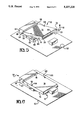
FIG. 1 is a plan view of an electronic card constructed according to this invention showing the shield in its first position.
FIG. 2 is a plan view of the electronic card of FIG. 1 with the shield in its second position.
FIG. 3 is a perspective view showing the electronic card and connector assembly according to this invention, with the electronic card shown inverted to expose its operative portion;
FIG. 4 is a side view of the electronic card and connector assembly according to this invention showing the electronic card about to be inserted in the hollow casing;
FIG. 5 is a perspective view showing the electronic card inserted in the hollow casing before the casing is pivoted toward the base member;
FIG. 6 is a perspective view showing the electronic card inserted in the casing with the casing pivoted toward the base member and latched in position;
FIG. 7 is a side view of the electronic card and connector assembly in the position shown in FIG. 6; and FIG. 8 is a cross sectional view of the casing taken along the lines 8--8 in FIG. 4.
Referring now to the drawings, an electronic card constructed according to this invention is designated generally by the reference numeral 10. The card 10 includes a housing 12 which contains integrated circuitry. The housing 12 has a first generally rectangular major surface 14, a second generally rectangular major surface 16 (FIG. 5) and four generally rectangular minor edge surfaces 18, 20, 22, 24 joining the first and second major surfaces 14, 16. The dimensions of the major surfaces 14, 16 are substantially the same as those of a standard credit card.
A plurality of contact pads electrically connected to the circuitry within the housing 12 is exposed on the surface 14 within a defined area. Thus, the contact pads could be directly on the surface 14 or, alternatively, could be on an internal printed wiring board with exposure through an opening in the surface 14. Preferably, the plurality of contact pads includes a first group of power and ground pads 26 and a second group of signal pads 28. The power and ground pads 26 are closer than the signal pads 28 to the edge surface 18 and are separated from the signal pads 28 by a region 30 of the surface 14 having no contact pads thereon. Illustratively, the signal pads 28 form an array of 240 pads arranged as six rows of forty positions in a staggered fifty by fifty mil grid.
The card 10 further includes a shield 32 which is mounted to the housing 12 overlying the surface 14 and movable between first and second positions. The shield 32 is arranged so that when it is in its first position, as shown in FIG. 1, all of the contact pads 26, 28 are covered by the shield 32 and when the shield 32 is in its second position, as shown in FIG. 2, all of the contact pads 26, 28 are exposed. Preferably, the shield 32 is formed with a window 34 of sufficient size and so located on the shield 32 that when the shield 32 is in its first position, the window 34 exposes the region 30 having no contact pads, as shown in FIG. 1, and when the shield 32 is in its second position, the window 34 exposes the signal pads 28 and has moved away from the power and ground pads 26 so that they are likewise exposed, as shown in FIG. 2. Also as shown in FIGS. 1 and 2, when in its first position the shield 32 is closer to the edge surface 18 than when it is in its second position.
The shield 32 may be made of either metal or plastic and is preferably mounted to the housing 12 in a manner similar to the mounting of the shield on a standard 31/2 inch floppy disk. Part of this mounting includes a spring member 36 (FIG. 4) disposed in a recess 38 on the minor edge surface 20 of the housing 12. The spring men, her 36 is connected at one end 40 to the shield 32 so as to yieldably bias the shield 32 toward its first position.
For alignment purposes, as will be described in full detail hereinafter, the shield 32 is notched at 42 and the housing 12 is formed with a pair of cavities 44 on its minor edge surfaces 20, 24. As shown in FIG. 1, when the shield 32 is in its first position, the cavities 44 are covered by the shield 32. As shown in FIG. 2, when the shield 32 is in its second position where the contact pads 26, 28 are exposed, the cavities 44 are aligned with the notches 42.
The electronic card 10 which has been described is of no use unless it can be electrically connected to a printed circuit board. FIGS. 3-8 illustrate a connector assembly, designated generally by the reference numeral 50, designed to electrically connect the electronic card 10 with a printed circuit board 52 having a surface array of contact pads 54. The connector assembly 50 includes a base member 56 which has a first planar surface 58 in contact with the printed circuit board 52 and an opposed second planar surface 60. The base member 56 is secured to the printed circuit board 52 in any desired manner, such as by screws or bolts (not shown). Disposed within suitable retention cavities 61 in the base member 56 is a plurality of contact members. The contact members are divided into a first group of power and ground contact members 62 and a second group of signal contact members 64. The power and ground contact members 62 correspond to the power and ground pads 66 on the electronic card 10 and the signal contact members 64 correspond to the signal pads 28 on the electronic card 10. As is conventional, each of the contact members 62, 64 is in electrical contact with a respective one of the printed circuit board pads 54 and is exposed at the base member second surface 60.
The connector assembly 50 also includes a hollow casing 66. The casing 66 has a first generally rectangular major side 68, a second generally rectangular major side 70, and four generally rectangular minor edge sides 72, 74, 76, 78 joining the major sides 68, 70. The interior of the casing 66 is sized so that at least a portion of the electronic card 10 can be accommodated therein. That portion of the electronic card 10 includes the contact pads 26, 28. To enable the electronic card 10 to be inserted into the interior of the casing 66, the minor edge side 72 of the casing 66 is formed with an opening 80 of sufficient size to receive the electronic card 10 therethrough. Further, the major side 68 of the casing 66 has an opening 82 (FIG. 8) sized and located so that when the electronic card 10 is seated within the casing 66, the contact pads 26, 28 are registered within the opening 82.
To move the shield 32 from its first position to its second position against the biasing force of the spring 36 when the electronic card 10 is inserted in the casing 66, the interiors of the minor edge sides 74, 78 of the casing 66 are formed with interference shoulders 84 and 86, respectively. As the electronic card 10 is inserted through the opening 80 and moved inwardly into the interior of the casing 66, the card housing 12 passes by the shoulders 84 and 86, but the shoulders 84 and 86 interfere with the shield 32 so that the shield 32 is moved from its first position to its second position as the card 10 is fully seated within the casing 66.
To effect the interconnection of the contact pads 26, 28 on the electronic card 10 with the contact pads 64 on the printed circuit board 52, the casing 66 is pivotably mounted to the base member 56. Toward this end, the casing 66 is formed with a pair of ears 88, 90 which are extensions of the minor edge sides 74 and 78, respectively, beyond the minor edge side 76. These ears 88, 90 flank an upstanding portion 92 of the base member 56 and are provided with aligned openings 94 and 96, respectively, for accommodating pivot pins therethrough which extend into the upstanding portion 92 to define a pivot axis 97 (FIG. 6) for the casing 66. Thus, when the casing 66 is pivoted so that its major side 68 goes toward the base member surface 60 and becomes parallel thereto, the opening 82 in the side 68 comes into registration with and surrounds the exposed contact members 62 and 64. With the electronic card 10 installed in the casing 66, after such pivoting the electronic card contact pads 26 and 28 engage the contact members 62, 64, respectively.
As disclosed herein, when the electronic card 10 is installed within the casing 66, its power and ground pads 26 are closer than the signal pads 28 to the pivot axis 97 of the casing 66. Likewise, the power and ground contact members 62 are closer than the signal contact members 64 to the pivot axis 97 of the casing 66. Accordingly, the power and ground pads 26 engages the power and ground contact members 62 before the signal pads 26 engage the signal contact members 64 when the casing 66 is pivoted toward the base member 56. Conversely, as the casing 66 is pivoted away from the base member 56, the signal pads 28 disengages from the signal contact members 64 before the power and ground pads 26 disengage from the power and ground contact members 62. Thus, as desired, the power and ground contacts "make" before the signal contacts connect and "break" after the signal contacts disconnect.
It is necessary to insure that as the casing 66 is pivoted toward the base member 56, the contact pads 26 and 28 are registered with respective ones of the contact members 62 and 64. Accordingly, secured to the base member 56 is a pair of spaced apart projections 98 and 100. These projections 98, 100 extend toward the casing 66. At least the major side 68 of the casing 66 is formed with a pair of openings 102 and 104 sized and spaced to receive the projections 98 and 100, respectively, therethrough as the casing 66 is pivoted toward the base member 56. As illustrated, the major side 70 of the casing 66 is also formed with a pair of openings 106 and 108 aligned with the openings 102 and 104, respectively, to also accept the projections 98, 100, respectively, therethrough. The openings 102, 104, 106 and 108 are aligned with the notches 42 and cavities 44 of the electronic card 10 when the electronic card 10 is fully seated within the interior of the casing 66. Thus, with the electronic card ! 0 so seated, when the casing 66 is pivoted toward the base member 56, the projections 98, 100 extend through the openings 102, 104, through the notches and cavities 42, 44 and through the openings 106, 108 to properly register the pads 26, 28 of the electronic card 10 with the contact members 62, 64. As shown in FIG. 7, the top of the upstanding portion 92 of the base member 56 is preferably aligned with the outer surface 110 of the equipment in which the electronic card 10 is to be installed. Mounted to such equipment, by means not shown, is a latch member 112. The latch 112 is resiliently biased toward the position shown in solid lines but is movable toward the position shown in broken lines. There is also preferably provided a resilient biasing means (spring) 116 (FIG. 4) for biasing the casing 66 counterclockwise about its pivot axis 97, as viewed in FIG. 7, so that it extends beyond the outer surface 110 of the equipment. This is similar to the arrangement in many present day audio cassette players. Thus, with the casing 66 so biased, the opening 82 on the minor edge side 72, which is remote from the pivot axis 97 of the casing 66, is exposed so that the electronic card 10 may be inserted into the casing 66. The casing 66 may then be pivoted clockwise against the force of the spring 116 until the outwardly extending end of the electronic card 10 engages the ramped surface 114 of the latch member 112. Continued pivoting of the casing 66 causes the latch member 112 to be moved toward the position shown in broken lines so that the electronic card 10 can pass thereby. The latch member 112 then returns to the position shown by the solid lines and retains the electronic card 10 and the casing 66 in their horizontal positions, as viewed in FIG. 7, with the pads 26, 28 engaged with the contact members 62, 64. When it is desired to remove the electronic card 10, the operator moves the latch member 112 toward the position shown in broken lines and the casing 66 "pops up" due to the action of the spring 116, thereby exposing the electronic card 10 for removal.
Accordingly, there has been disclosed an improved design for an electronic card and a connector assembly for use therewith. While an illustrative embodiment of the present invention has been disclosed herein, it is understood that various modifications and adaptations to the disclosed embodiment will be apparent to those of ordinary skill in the art and it is intended that this invention only be limited by the scope of the appended claims.
Claims (12)
1. An electronic card (10) containing integrated circuitry, comprising:
a housing (12) containing said circuitry, said housing having first (14) and second (16) generally rectangular major surfaces and four (18, 20, 22, 24) generally rectangular minor edge surfaces joining said first and second major surfaces;
a plurality of contact pads (26, 28) electrically connected to said circuitry and exposed on said first major surface of said housing within a defined area having a surface area; and
a shield (32) movable mounted to said housing overlying said first major surface wherein said shield is movable between first and second positions, said shield being arranged so that when said shield is in said first position said defined area is covered by said shield and when said shield is in said second position said defined area is exposed.
2. The card according to claim 1 wherein said shield is formed with a window (34) having a size at least as large as said surface area of said defined area and so located on said shield that when said shield is in said first position said defined area is covered by said shield and when said shield is in said second position said defined area is exposed through said shield window.
3. The card according to claim 1 wherein:
said plurality of contact pads includes a first group of power and ground pads (26) and a second group of signal pads (28), said first group of power and ground pads (26) being closer than said second group of signal pads (28) to a first (18) of said edge surfaces; and
said shield first position is closer than said shield second position to said first edge surface, and said shield is formed with a window (34) having a size area at least as large as said surface area of said defined area and so located on said shield that when said shield is in said second position said second group of signal pads (28) is exposed through said shield window.
4. The card according to claim 3 wherein said first and second groups of pads (26, 28) are separated from each other by a region (30) of said first major surface (14) having no contact pads, said region being exposed through said shield window (34) when said shield is in said first position.
5. The card according to claim 1 further including means (36) for yieldably biasing sad shield toward said first position.
6. A connector assembly (50) for electrically connecting a printed circuit board (52) having a surface array of contact pads (54) with an electronic card (10), said electronic card containing integrated circuitry and having a housing (12) containing said circuitry, said housing having first (14) and second (16) generally rectangular major surfaces and four (18, 20, 22, 24) generally rectangular edge surfaces joining said first and second major surfaces, a plurality of contact pads (26, 28) electrically connected to said circuitry and exposed on said first major surface (14) of said housing (12) within a defined area, and a shield (32) mounted to said housing overlying said first major surface and movable between first and second positions, said shield being arranged so that when said shield is in said first position said defined area is covered by said shield and when said shield is in said second position said defined area is exposed, the assembly comprising:
a base member (56) secured to said printed circuit board (52), said base member having a first planar surface (58) in contact with said printed circuit board and an opposed second planar surface (60);
a plurality of contact members (62, 64) disposed in said base member, each of said plurality of contact members being in electrical contact with a respective one of said printed circuit board contact pads and each of said plurality of contact members being exposed at said base member second surface;
a hollow casing (66), said casing having first (68) and second (70) generally rectangular major sides and four (72, 74, 76, 78) generally rectangular minor edge sides joining said first and second major sides, the interior of said casing being sized so that at least a portion of said electronic card with said defined area of said housing first major surface can be accommodated therein, one (72) of said casing minor edge sides having an opening (80) at least as large as one of the edge surfaces of the electronic card (10), and said casing first major side (68) having an opening (82) sized and located so that when said electronic card (10) is disposed within said casing said defined area of said housing first major surface (14) is registered within said casing first major side opening (82);
means (84, 86) in said casing (66) for moving said electronic card shield (32) from said first position to said second position when said electronic card (10) is inserted in said casing; and
means (88, 90, 84, 96) for mounting said casing (66) to said base member (56) for pivotal movement about a pivot axis so that said casing first major side (68) is movable toward and away from said base member second surface (60), said mounting means being arranged so that when casing first major side is pivoted toward said base member second surface and becomes parallel thereto said casing first major side opening (82) comes into registration with the exposed plurality of contact members (62, 64);
whereby when said electronic card is inserted in said casing and said casing is pivoted toward said base member, said plurality of electronic card contact pads (26, 28) engage said plurality of contact members (62, 64).
7. The assembly according to claim 6 wherein on said electronic card (10) said plurality of contact pads includes a first group of power and ground pads (26) and a second group of signal pads (28), said first group of power and ground pads being closer than said second group of signal pads to a first of said edge surfaces (18), said first of said edge surfaces being proximate said pivot axis when said electronic card is inserted in said casing, and wherein said plurality of contact members includes a first group of power and ground contact members (62) corresponding to the first group of power and ground pads (26) of said electronic card and a second group of signal contact members (64) corresponding to the second group of signal pads (28) of said electronic card, said first group of power and ground contact members being closer than said second group of signal contact members to said pivot axis;
whereby when said electronic card is inserted in said casing and said casing is pivoted toward said base member, said first group of power and ground pads of said electronic card engages said first group of power and ground contact members before said second group of signal pads of said electronic card engages said second group of signal contact members, and when said casing is pivoted away from said base member, said second group of signal pads of said electronic card disengages from said second group of signal contact members before said first group of power and ground pads of said electronic card disengages from said first group of power and ground contact members.
8. The assembly according to claim 6 further including means (98, 100, 42, 44, 102, 104, 106, 108) for registering said plurality of electronic card contact pads (26, 28) with respective ones of said plurality of contact members (62, 64) as said casing containing said electronic card is pivoted toward said base member.
9. The assembly according to claim 8 wherein said casing first major side (68) is formed with a pair of spaced openings (102, 104), said electronic card (10) is formed with a pair of cavities (44) which are aligned with said casing first major side spaced openings when said electronic card is inserted to a predetermined position within said casing, and said apparatus further includes a pair of projections (98, 100) secured to said base member (56) and adapted to each extend through a respective one of said casing first major side spaced openings and into a respective one of said electronic card cavities to effect the registration of said contact pads (26, 28) with said contact members (62, 64).
10. The assembly according to claim 6 wherein said pivot axis is remote from and parallel to said one of said casing minor edge sides (72).
11. The assembly according to claim 6 further including latching means (112) for releasably retaining said electronic card contact pads (26, 28) in engagement with said contact members (62, 64).
12. The assembly according to claim 11 further including means (116) for resiliently biasing said casing (66) away from said base member second surface (60).
Priority Applications (7)
| Application Number | Priority Date | Filing Date | Title |
|---|---|---|---|
| US08/119,784 US5337220A (en) | 1993-09-10 | 1993-09-10 | Electronic card and connector assembly for use therewith |
| TW082108918A TW222037B (en) | 1993-09-10 | 1993-10-27 | Electronic card and connector assembly for use therewith |
| KR1019940021354A KR100286565B1 (en) | 1993-09-10 | 1994-08-29 | Electronic card and connector assembly for use with it |
| GB9417904A GB2281823A (en) | 1993-09-10 | 1994-09-06 | Electronic card with shielded contacts and connector assembly for use therewith |
| DE4432028A DE4432028A1 (en) | 1993-09-10 | 1994-09-08 | Electronics card and connector assembly for use with this |
| CN94192104A CN1048144C (en) | 1993-09-10 | 1994-09-10 | Electronic card and connector assembly for use therewith |
| JP6243332A JPH07121670A (en) | 1993-09-10 | 1994-09-12 | Electronic card and connector assembly for electronic card |
Applications Claiming Priority (1)
| Application Number | Priority Date | Filing Date | Title |
|---|---|---|---|
| US08/119,784 US5337220A (en) | 1993-09-10 | 1993-09-10 | Electronic card and connector assembly for use therewith |
Publications (1)
| Publication Number | Publication Date |
|---|---|
| US5337220A true US5337220A (en) | 1994-08-09 |
Family
ID=22386386
Family Applications (1)
| Application Number | Title | Priority Date | Filing Date |
|---|---|---|---|
| US08/119,784 Expired - Fee Related US5337220A (en) | 1993-09-10 | 1993-09-10 | Electronic card and connector assembly for use therewith |
Country Status (7)
| Country | Link |
|---|---|
| US (1) | US5337220A (en) |
| JP (1) | JPH07121670A (en) |
| KR (1) | KR100286565B1 (en) |
| CN (1) | CN1048144C (en) |
| DE (1) | DE4432028A1 (en) |
| GB (1) | GB2281823A (en) |
| TW (1) | TW222037B (en) |
Cited By (44)
| Publication number | Priority date | Publication date | Assignee | Title |
|---|---|---|---|---|
| US5425651A (en) * | 1994-03-04 | 1995-06-20 | The Whitaker Corporation | Card edge connector providing non-simultaneous electrical connections |
| US5535342A (en) * | 1992-11-05 | 1996-07-09 | Giga Operations Corporation | Pld connector for module having configuration of either first PLD or second PLD and reconfigurable bus for communication of two different bus protocols |
| US5537293A (en) * | 1993-12-28 | 1996-07-16 | Nec Corporation | IC card having an electronic apparatus |
| US5641314A (en) * | 1995-06-30 | 1997-06-24 | The Whitaker Corporation | Memory card receptacle connector and contact terminal |
| US5642259A (en) * | 1996-01-31 | 1997-06-24 | Ma; Hsi-Kuang | Arrangement for connecting an expansion card to a connector socket in a personal computer |
| USD382297S (en) * | 1996-02-28 | 1997-08-12 | Hewlett-Packard Company | Infrared communication port for a portable inkjet printer |
| US5662482A (en) * | 1994-11-17 | 1997-09-02 | Samsung Electronics Co., Ltd. | PCMCIA connector having a protection cover |
| US5712766A (en) * | 1996-10-17 | 1998-01-27 | Minnesota Mining And Manufacturing Company | One-piece housing and interlocking connector for IC card assemblies |
| US5731629A (en) * | 1995-03-10 | 1998-03-24 | Data-Disk Technology, Inc. | Personal memory devices carried by an individual which can be read and written to |
| US5757622A (en) * | 1996-11-13 | 1998-05-26 | Sharp Kabushiki Kaisha | Connecting structure for electronic equipment |
| US5781232A (en) * | 1993-12-28 | 1998-07-14 | Nikon Corporation | Recording medium insertion and removal mechanism |
| US5961338A (en) * | 1996-01-04 | 1999-10-05 | Hon Hai Precision Ind. Co., Ltd. | IC card connector |
| EP0959423A2 (en) * | 1998-05-18 | 1999-11-24 | Yamaichi Electronics Co., Ltd. | Card connector |
| US6002589A (en) * | 1997-07-21 | 1999-12-14 | Rambus Inc. | Integrated circuit package for coupling to a printed circuit board |
| US6004142A (en) * | 1997-03-04 | 1999-12-21 | Micron Technology, Inc. | Interposer converter to allow single-sided contact to circuit modules |
| US6027365A (en) * | 1998-05-28 | 2000-02-22 | The Whitaker Corporation | Test card receptacle and header |
| US6089882A (en) * | 1996-11-27 | 2000-07-18 | The Whitaker Corporation | Memory card connector with grounding clip |
| US6234820B1 (en) * | 1997-07-21 | 2001-05-22 | Rambus Inc. | Method and apparatus for joining printed circuit boards |
| US6270369B1 (en) * | 1999-04-15 | 2001-08-07 | International Business Machines Corporation | Sub-card board connector, sub-card board, modem sub-card, and a computer having this connector |
| US6300563B1 (en) * | 1998-11-10 | 2001-10-09 | Daimlerchrysler Corporation | Gauge assembly having an adaptable coil assembly |
| US6493033B1 (en) | 1998-12-09 | 2002-12-10 | Eastman Kodak Company | Electronic apparatus adapted to receive a memory card |
| US6498729B2 (en) * | 2000-03-03 | 2002-12-24 | Hewlett-Packard Company | Expansion module |
| US6510057B2 (en) * | 2001-04-12 | 2003-01-21 | Hewlett-Packard Company | Computing device with a card receptacle |
| US20030190832A1 (en) * | 2002-04-09 | 2003-10-09 | Japan Aviation Electronics Industry, Limited | Card connector reduced in operating force |
| EP1365480A1 (en) * | 2001-02-02 | 2003-11-26 | J.S.T. Mfg. Co., Ltd. | Flash memory card connector |
| US6667889B2 (en) * | 2002-01-07 | 2003-12-23 | Hewlett-Packard Development Company, L.P. | System and method for pivotal installation and removal of a circuit board from a chassis |
| US6710614B1 (en) | 1997-03-04 | 2004-03-23 | Micron Technology, Inc. | Methods for using an interposer/converter to allow single-sided contact to circuit modules |
| DE10308100A1 (en) * | 2003-02-26 | 2004-09-09 | Conti Temic Microelectronic Gmbh | Housing for sensor used to trigger airbag, has inner housing inserted into outer housing which is fixed in holding frame by locking hooks |
| US6822878B2 (en) * | 2002-10-09 | 2004-11-23 | Hewlett-Packard Development Company, L.P. | Circuit board support arrangement, method, and method for using the same |
| US6826638B1 (en) * | 1999-07-15 | 2004-11-30 | Dell Products L.P. | Modular bay enclosure removable card method and system |
| US20050064748A1 (en) * | 2003-09-19 | 2005-03-24 | Qisheng Zheng | SIM card connector |
| US20050070171A1 (en) * | 2003-09-30 | 2005-03-31 | Qisheng Zheng | SIM card connector |
| US20050245136A1 (en) * | 2004-04-29 | 2005-11-03 | Hao Yin | Memory card connector with metal cover and ground terminals |
| WO2007044219A2 (en) * | 2005-10-06 | 2007-04-19 | Motorola, Inc. | Integrated selectively angled camera for clam style products |
| US20070097663A1 (en) * | 2005-11-02 | 2007-05-03 | Partick Wallace | Card holder arrangement for circuit assembly |
| US20070243748A1 (en) * | 2006-04-18 | 2007-10-18 | Brother Kogyo Kabushiki Kaisha | Image forming apparatus and multi-function device |
| US20100073891A1 (en) * | 2008-09-25 | 2010-03-25 | Shenzhen Futaihong Precision Industry Co., Ltd. | Chip card holder and portable electronic device using the same |
| US20100112838A1 (en) * | 2008-10-31 | 2010-05-06 | Shenzhen Futaihong Precision Industry Co., Ltd. | Card socket assembly |
| US20100227491A1 (en) * | 2009-03-03 | 2010-09-09 | Au Optronics Corp. | Electrical Connector |
| US20110075379A1 (en) * | 2009-09-29 | 2011-03-31 | Hong Fu Jin Precision Industry (Shenzhen) Co., Ltd. | Electronic device with a covered expansion card bay |
| WO2013082189A3 (en) * | 2011-11-29 | 2013-08-08 | Apple Inc. | Folding so-dimm socket |
| US20140349515A1 (en) * | 2012-01-20 | 2014-11-27 | Saint-Gobain Glass France | Connection element |
| US20150340780A1 (en) * | 2012-11-30 | 2015-11-26 | Compagnie Industrielle Et Financiere D'ingenierie "Ingenico" | Flap for Terminal |
| US20170027076A1 (en) * | 2013-06-26 | 2017-01-26 | Zodiac Aero Electric | Electrical equipment comprising electronic cards |
Families Citing this family (12)
| Publication number | Priority date | Publication date | Assignee | Title |
|---|---|---|---|---|
| DE29506013U1 (en) * | 1995-04-07 | 1996-08-08 | Stocko Metallwarenfab Henkels | Holding device for card-shaped support elements |
| DE29607253U1 (en) * | 1996-04-22 | 1996-07-04 | Stocko Metallwarenfab Henkels | Combi chip card reader |
| DE29811425U1 (en) * | 1998-06-29 | 1998-09-17 | Stocko Metallwarenfab Henkels | Contact unit for a card-shaped carrier element of electronic assemblies, in particular according to the PCMCIA standard |
| DE19922976A1 (en) * | 1999-05-19 | 2000-12-07 | Bosch Gmbh Robert | Device and method for holding cards on a device housing |
| DE10013843A1 (en) | 2000-03-15 | 2001-11-29 | Infineon Technologies Ag | Connection system |
| JP3472526B2 (en) * | 2000-04-27 | 2003-12-02 | 日本圧着端子製造株式会社 | Connection module for integrated circuit element and integrated circuit element with connection module |
| DE10241972A1 (en) * | 2002-09-10 | 2004-03-18 | Tenovis Gmbh & Co. Kg | Telecommunications unit has additional clip on wedge shaped module for new USB, Bluetooth (RTM), speech and loudspeaker functions |
| US6791843B1 (en) * | 2003-06-11 | 2004-09-14 | Hewlett-Packard Development Company, L.P. | Parallel board connection system and method |
| JP4760667B2 (en) * | 2006-10-27 | 2011-08-31 | ソニー株式会社 | Data protection device |
| DE102009048934B4 (en) * | 2009-04-24 | 2014-07-24 | Abb Ag | Arrangement for covering the edge contact surface of a printed circuit board and Kontaktflächen- cover |
| CN109449677B (en) * | 2018-10-30 | 2020-09-18 | 出门问问信息科技有限公司 | Alignment auxiliary device |
| KR102282452B1 (en) * | 2019-03-05 | 2021-07-27 | 한화정밀기계 주식회사 | Component imaging apparatus |
Citations (12)
| Publication number | Priority date | Publication date | Assignee | Title |
|---|---|---|---|---|
| US3701071A (en) * | 1971-01-18 | 1972-10-24 | Berg Electronics Inc | Hinge type circuit board connector block |
| US3848952A (en) * | 1973-07-27 | 1974-11-19 | Amp Inc | Zero insertion force edge card connector |
| US4677527A (en) * | 1984-07-09 | 1987-06-30 | International Business Machines Corp. | Compact electrical connection and distribution system for pluggable modular devices |
| US4678252A (en) * | 1986-05-27 | 1987-07-07 | Rockwell International Corporation | Electrical connector for circuit boards |
| US4838806A (en) * | 1986-02-05 | 1989-06-13 | Molex Incorporated | Electrical connector |
| US5031076A (en) * | 1988-12-06 | 1991-07-09 | E. I. Du Pont De Nemours And Company | Multifunctional card having a static protection |
| US5052942A (en) * | 1989-12-21 | 1991-10-01 | Stocko Metallwarenfabriken Henkels Und Sohn Gmbh & Co. | Device for electrically contacting a printed circuit board with an electronic card, especially an IC-memory card, that has contacting poles along one of its sides |
| US5088929A (en) * | 1990-06-22 | 1992-02-18 | Molex Incorporated | Board-to-board connecton type electric connector |
| US5154618A (en) * | 1991-09-30 | 1992-10-13 | Amp Incorporated | Electrical assembly |
| JPH0517720A (en) * | 1991-07-16 | 1993-01-26 | Toshiba Silicone Co Ltd | Incombustible coating paint for electronic part, its production and electronic part coated with incombustible paint |
| US5186651A (en) * | 1991-01-29 | 1993-02-16 | Firma Karl Lumberg Gmbh & Co. | Plug connector, especially for the releasable connection of electrical conductors |
| US5197888A (en) * | 1992-02-25 | 1993-03-30 | International Business Machines Corporation | Method of positioning flexible circuit members on a common circuit member |
Family Cites Families (6)
| Publication number | Priority date | Publication date | Assignee | Title |
|---|---|---|---|---|
| JPS59162676A (en) * | 1983-03-08 | 1984-09-13 | Canon Inc | Electronic apparatus |
| US4602351A (en) * | 1983-07-06 | 1986-07-22 | Tokyo Tatsuno Co., Ltd. | Device for reading and writing IC-external storage cards |
| JPS60179982A (en) * | 1984-02-28 | 1985-09-13 | Canon Inc | External memory pack |
| JP2534204B2 (en) * | 1987-03-31 | 1996-09-11 | 三菱電機株式会社 | Semiconductor device card |
| JPH0775030B2 (en) * | 1987-08-07 | 1995-08-09 | 沖電気工業株式会社 | Card type integrated circuit connector |
| JPH0164864U (en) * | 1987-10-21 | 1989-04-26 |
-
1993
- 1993-09-10 US US08/119,784 patent/US5337220A/en not_active Expired - Fee Related
- 1993-10-27 TW TW082108918A patent/TW222037B/en active
-
1994
- 1994-08-29 KR KR1019940021354A patent/KR100286565B1/en not_active IP Right Cessation
- 1994-09-06 GB GB9417904A patent/GB2281823A/en not_active Withdrawn
- 1994-09-08 DE DE4432028A patent/DE4432028A1/en not_active Withdrawn
- 1994-09-10 CN CN94192104A patent/CN1048144C/en not_active Expired - Fee Related
- 1994-09-12 JP JP6243332A patent/JPH07121670A/en active Pending
Patent Citations (12)
| Publication number | Priority date | Publication date | Assignee | Title |
|---|---|---|---|---|
| US3701071A (en) * | 1971-01-18 | 1972-10-24 | Berg Electronics Inc | Hinge type circuit board connector block |
| US3848952A (en) * | 1973-07-27 | 1974-11-19 | Amp Inc | Zero insertion force edge card connector |
| US4677527A (en) * | 1984-07-09 | 1987-06-30 | International Business Machines Corp. | Compact electrical connection and distribution system for pluggable modular devices |
| US4838806A (en) * | 1986-02-05 | 1989-06-13 | Molex Incorporated | Electrical connector |
| US4678252A (en) * | 1986-05-27 | 1987-07-07 | Rockwell International Corporation | Electrical connector for circuit boards |
| US5031076A (en) * | 1988-12-06 | 1991-07-09 | E. I. Du Pont De Nemours And Company | Multifunctional card having a static protection |
| US5052942A (en) * | 1989-12-21 | 1991-10-01 | Stocko Metallwarenfabriken Henkels Und Sohn Gmbh & Co. | Device for electrically contacting a printed circuit board with an electronic card, especially an IC-memory card, that has contacting poles along one of its sides |
| US5088929A (en) * | 1990-06-22 | 1992-02-18 | Molex Incorporated | Board-to-board connecton type electric connector |
| US5186651A (en) * | 1991-01-29 | 1993-02-16 | Firma Karl Lumberg Gmbh & Co. | Plug connector, especially for the releasable connection of electrical conductors |
| JPH0517720A (en) * | 1991-07-16 | 1993-01-26 | Toshiba Silicone Co Ltd | Incombustible coating paint for electronic part, its production and electronic part coated with incombustible paint |
| US5154618A (en) * | 1991-09-30 | 1992-10-13 | Amp Incorporated | Electrical assembly |
| US5197888A (en) * | 1992-02-25 | 1993-03-30 | International Business Machines Corporation | Method of positioning flexible circuit members on a common circuit member |
Non-Patent Citations (1)
| Title |
|---|
| PCMCIA Backgrounder (no date provided). * |
Cited By (73)
| Publication number | Priority date | Publication date | Assignee | Title |
|---|---|---|---|---|
| US5535342A (en) * | 1992-11-05 | 1996-07-09 | Giga Operations Corporation | Pld connector for module having configuration of either first PLD or second PLD and reconfigurable bus for communication of two different bus protocols |
| US5781232A (en) * | 1993-12-28 | 1998-07-14 | Nikon Corporation | Recording medium insertion and removal mechanism |
| US5537293A (en) * | 1993-12-28 | 1996-07-16 | Nec Corporation | IC card having an electronic apparatus |
| US5425651A (en) * | 1994-03-04 | 1995-06-20 | The Whitaker Corporation | Card edge connector providing non-simultaneous electrical connections |
| US5662482A (en) * | 1994-11-17 | 1997-09-02 | Samsung Electronics Co., Ltd. | PCMCIA connector having a protection cover |
| US5731629A (en) * | 1995-03-10 | 1998-03-24 | Data-Disk Technology, Inc. | Personal memory devices carried by an individual which can be read and written to |
| US5641314A (en) * | 1995-06-30 | 1997-06-24 | The Whitaker Corporation | Memory card receptacle connector and contact terminal |
| US5961338A (en) * | 1996-01-04 | 1999-10-05 | Hon Hai Precision Ind. Co., Ltd. | IC card connector |
| US5642259A (en) * | 1996-01-31 | 1997-06-24 | Ma; Hsi-Kuang | Arrangement for connecting an expansion card to a connector socket in a personal computer |
| USD382297S (en) * | 1996-02-28 | 1997-08-12 | Hewlett-Packard Company | Infrared communication port for a portable inkjet printer |
| US5712766A (en) * | 1996-10-17 | 1998-01-27 | Minnesota Mining And Manufacturing Company | One-piece housing and interlocking connector for IC card assemblies |
| US5757622A (en) * | 1996-11-13 | 1998-05-26 | Sharp Kabushiki Kaisha | Connecting structure for electronic equipment |
| US6089882A (en) * | 1996-11-27 | 2000-07-18 | The Whitaker Corporation | Memory card connector with grounding clip |
| US6004142A (en) * | 1997-03-04 | 1999-12-21 | Micron Technology, Inc. | Interposer converter to allow single-sided contact to circuit modules |
| US6710614B1 (en) | 1997-03-04 | 2004-03-23 | Micron Technology, Inc. | Methods for using an interposer/converter to allow single-sided contact to circuit modules |
| US6200144B1 (en) | 1997-03-04 | 2001-03-13 | Micron Technology, Inc. | Interposer/converter to allow single-sided contact to circuit modules |
| US6002589A (en) * | 1997-07-21 | 1999-12-14 | Rambus Inc. | Integrated circuit package for coupling to a printed circuit board |
| US6234820B1 (en) * | 1997-07-21 | 2001-05-22 | Rambus Inc. | Method and apparatus for joining printed circuit boards |
| US6447321B1 (en) | 1997-07-21 | 2002-09-10 | Rambus, Inc. | Socket for coupling an integrated circuit package to a printed circuit board |
| EP0959423A2 (en) * | 1998-05-18 | 1999-11-24 | Yamaichi Electronics Co., Ltd. | Card connector |
| EP0959423A3 (en) * | 1998-05-18 | 1999-12-08 | Yamaichi Electronics Co., Ltd. | Card connector |
| US6227893B1 (en) | 1998-05-18 | 2001-05-08 | Yamaichi Electronics Co., Ltd. | Card connector |
| US6027365A (en) * | 1998-05-28 | 2000-02-22 | The Whitaker Corporation | Test card receptacle and header |
| US6300563B1 (en) * | 1998-11-10 | 2001-10-09 | Daimlerchrysler Corporation | Gauge assembly having an adaptable coil assembly |
| US6493033B1 (en) | 1998-12-09 | 2002-12-10 | Eastman Kodak Company | Electronic apparatus adapted to receive a memory card |
| US6270369B1 (en) * | 1999-04-15 | 2001-08-07 | International Business Machines Corporation | Sub-card board connector, sub-card board, modem sub-card, and a computer having this connector |
| US6826638B1 (en) * | 1999-07-15 | 2004-11-30 | Dell Products L.P. | Modular bay enclosure removable card method and system |
| US6498729B2 (en) * | 2000-03-03 | 2002-12-24 | Hewlett-Packard Company | Expansion module |
| US7066766B2 (en) | 2001-02-02 | 2006-06-27 | J.S.T. Mfg. Co., Ltd. | Flash memory card connector |
| EP1365480A4 (en) * | 2001-02-02 | 2005-04-27 | J S T Mfg Co Ltd | Flash memory card connector |
| EP1365480A1 (en) * | 2001-02-02 | 2003-11-26 | J.S.T. Mfg. Co., Ltd. | Flash memory card connector |
| US20040087211A1 (en) * | 2001-02-02 | 2004-05-06 | Masaaki Harasawa | Flash memory card connector |
| US6510057B2 (en) * | 2001-04-12 | 2003-01-21 | Hewlett-Packard Company | Computing device with a card receptacle |
| US20050024836A1 (en) * | 2002-01-07 | 2005-02-03 | Jansen Kenneth A. | System and method for pivotal installation and removal of a circuit board from a chassis |
| US6667889B2 (en) * | 2002-01-07 | 2003-12-23 | Hewlett-Packard Development Company, L.P. | System and method for pivotal installation and removal of a circuit board from a chassis |
| US6970361B2 (en) | 2002-01-07 | 2005-11-29 | Hewlett-Packard Development Company, L.P. | System and method for pivotal installation and removal of a circuit board from a chassis |
| US20030190832A1 (en) * | 2002-04-09 | 2003-10-09 | Japan Aviation Electronics Industry, Limited | Card connector reduced in operating force |
| EP1355384A3 (en) * | 2002-04-09 | 2004-09-08 | Japan Aviation Electronics Industry, Limited | Card connector reduced in operating force |
| EP1355384A2 (en) * | 2002-04-09 | 2003-10-22 | Japan Aviation Electronics Industry, Limited | Card connector reduced in operating force |
| US6890203B2 (en) | 2002-04-09 | 2005-05-10 | Japan Aviation Electronics Industry, Limited | Card connector reduced in operating force |
| US6822878B2 (en) * | 2002-10-09 | 2004-11-23 | Hewlett-Packard Development Company, L.P. | Circuit board support arrangement, method, and method for using the same |
| DE10308100A1 (en) * | 2003-02-26 | 2004-09-09 | Conti Temic Microelectronic Gmbh | Housing for sensor used to trigger airbag, has inner housing inserted into outer housing which is fixed in holding frame by locking hooks |
| US20050064748A1 (en) * | 2003-09-19 | 2005-03-24 | Qisheng Zheng | SIM card connector |
| US20050070171A1 (en) * | 2003-09-30 | 2005-03-31 | Qisheng Zheng | SIM card connector |
| US6974343B2 (en) * | 2003-09-30 | 2005-12-13 | Hon Hai Precision Ind. Co., Ltd. | SIM card connector |
| US20050245136A1 (en) * | 2004-04-29 | 2005-11-03 | Hao Yin | Memory card connector with metal cover and ground terminals |
| WO2007044219A2 (en) * | 2005-10-06 | 2007-04-19 | Motorola, Inc. | Integrated selectively angled camera for clam style products |
| WO2007044219A3 (en) * | 2005-10-06 | 2007-09-20 | Motorola Inc | Integrated selectively angled camera for clam style products |
| US7425100B2 (en) | 2005-10-06 | 2008-09-16 | Motorola, Inc. | Integrated selectively angled camera for clam style products |
| US20070097663A1 (en) * | 2005-11-02 | 2007-05-03 | Partick Wallace | Card holder arrangement for circuit assembly |
| US7623357B2 (en) * | 2005-11-02 | 2009-11-24 | Symbol Technologies, Inc. | Card holder arrangement for circuit assembly |
| US20070243748A1 (en) * | 2006-04-18 | 2007-10-18 | Brother Kogyo Kabushiki Kaisha | Image forming apparatus and multi-function device |
| US7705873B2 (en) * | 2006-04-18 | 2010-04-27 | Brother Kogyo Kabushiki Kaisha | Image forming apparatus and multi-function device |
| US20100073891A1 (en) * | 2008-09-25 | 2010-03-25 | Shenzhen Futaihong Precision Industry Co., Ltd. | Chip card holder and portable electronic device using the same |
| US8199480B2 (en) * | 2008-09-25 | 2012-06-12 | Shenzhen Futaihong Precision Industry Co., Ltd. | Chip card holder and portable electronic device using the same |
| US7762827B2 (en) * | 2008-10-31 | 2010-07-27 | Shenzhen Futaihong Precision Industry Co., Ltd. | Card assembly with a hinged cover including a torsion spring |
| US20100112838A1 (en) * | 2008-10-31 | 2010-05-06 | Shenzhen Futaihong Precision Industry Co., Ltd. | Card socket assembly |
| US20100227491A1 (en) * | 2009-03-03 | 2010-09-09 | Au Optronics Corp. | Electrical Connector |
| US7976328B2 (en) * | 2009-03-03 | 2011-07-12 | Au Optronics Corp. | Electrical connector |
| CN102036519B (en) * | 2009-09-29 | 2014-10-15 | 鸿富锦精密工业(深圳)有限公司 | Electronic device |
| US20110075379A1 (en) * | 2009-09-29 | 2011-03-31 | Hong Fu Jin Precision Industry (Shenzhen) Co., Ltd. | Electronic device with a covered expansion card bay |
| CN102036519A (en) * | 2009-09-29 | 2011-04-27 | 鸿富锦精密工业(深圳)有限公司 | Electronic device |
| US8254105B2 (en) * | 2009-09-29 | 2012-08-28 | Hong Fu Jin Precision Industry (Shenzhen) Co., Ltd. | Electronic device with a covered expansion card bay |
| WO2013082189A3 (en) * | 2011-11-29 | 2013-08-08 | Apple Inc. | Folding so-dimm socket |
| KR20140098210A (en) * | 2011-11-29 | 2014-08-07 | 애플 인크. | Folding so-dimm socket |
| US8968019B2 (en) | 2011-11-29 | 2015-03-03 | Apple Inc. | Folding SO-DIMM socket |
| US9537238B2 (en) | 2011-11-29 | 2017-01-03 | Apple Inc. | Folding SO-DIMM socket |
| US20140349515A1 (en) * | 2012-01-20 | 2014-11-27 | Saint-Gobain Glass France | Connection element |
| US9509088B2 (en) * | 2012-01-20 | 2016-11-29 | Saint-Gobain Glass France | Connection element |
| US20150340780A1 (en) * | 2012-11-30 | 2015-11-26 | Compagnie Industrielle Et Financiere D'ingenierie "Ingenico" | Flap for Terminal |
| US9680242B2 (en) * | 2012-11-30 | 2017-06-13 | Ingenico Group | Flap for terminal |
| US20170027076A1 (en) * | 2013-06-26 | 2017-01-26 | Zodiac Aero Electric | Electrical equipment comprising electronic cards |
| US9980406B2 (en) * | 2013-06-26 | 2018-05-22 | Zodiac Aero Electric | Electrical equipment comprising electronic cards |
Also Published As
| Publication number | Publication date |
|---|---|
| GB9417904D0 (en) | 1994-10-26 |
| CN1048144C (en) | 2000-01-05 |
| KR950010190A (en) | 1995-04-26 |
| KR100286565B1 (en) | 2001-04-16 |
| TW222037B (en) | 1994-04-01 |
| DE4432028A1 (en) | 1995-03-16 |
| JPH07121670A (en) | 1995-05-12 |
| CN1104382A (en) | 1995-06-28 |
| GB2281823A (en) | 1995-03-15 |
Similar Documents
| Publication | Publication Date | Title |
|---|---|---|
| US5337220A (en) | Electronic card and connector assembly for use therewith | |
| KR970002362B1 (en) | Connector | |
| US6097605A (en) | Contacting unit for card-shaped support elements for electronic components | |
| US5734551A (en) | Method to install SIMMs without causing discomfort to the user | |
| US5401176A (en) | Connector device | |
| JP3306831B2 (en) | Small card docking connector | |
| KR100318123B1 (en) | Smart card computer adapter | |
| US6761572B1 (en) | Mini memory card connector | |
| GB2369600A (en) | A system configuration or smart card with a notch for security | |
| EP1318568B1 (en) | Connector with shutter | |
| JP3097154U (en) | Connector structure for multiple storage media | |
| JP3279443B2 (en) | Data recording / reproducing device | |
| JPS63176193A (en) | Information card | |
| JP3835353B2 (en) | Adapter for card connection | |
| KR100238909B1 (en) | Ic card reading/writing device | |
| JPH09185975A (en) | Card-in type shield connector | |
| JP2002352212A (en) | Cf card | |
| JPH08510583A (en) | Device for exchanging information with an electrical memory card and car radio equipped with such a device | |
| JP2004259051A (en) | Connector device for card | |
| JP2001256466A (en) | Memory card mounting system | |
| JP3045020U (en) | Memory card case | |
| KR200325361Y1 (en) | 2-in-1 connector structure for multi-storage media | |
| JP2003132977A (en) | Connector apparatus for card | |
| JPH10189141A (en) | Connector for card | |
| KR200322549Y1 (en) | Coupling apparatus for a connector |
Legal Events
| Date | Code | Title | Description |
|---|---|---|---|
| AS | Assignment |
Owner name: WHITAKER CORPORATION, THE, CALIFORNIA Free format text: ASSIGNMENT OF ASSIGNORS INTEREST;ASSIGNOR:GRANITZ, RICHARD F.;REEL/FRAME:006700/0249 Effective date: 19930908 |
|
| FPAY | Fee payment |
Year of fee payment: 4 |
|
| REMI | Maintenance fee reminder mailed | ||
| LAPS | Lapse for failure to pay maintenance fees | ||
| STCH | Information on status: patent discontinuation |
Free format text: PATENT EXPIRED DUE TO NONPAYMENT OF MAINTENANCE FEES UNDER 37 CFR 1.362 |
|
| FP | Lapsed due to failure to pay maintenance fee |
Effective date: 20020809 |