EP0957534A1 - Vorrichtung zum Senden und Empfangen von zirkularpolarisierten Hochfrequenzwellen - Google Patents
Vorrichtung zum Senden und Empfangen von zirkularpolarisierten Hochfrequenzwellen Download PDFInfo
- Publication number
- EP0957534A1 EP0957534A1 EP99401148A EP99401148A EP0957534A1 EP 0957534 A1 EP0957534 A1 EP 0957534A1 EP 99401148 A EP99401148 A EP 99401148A EP 99401148 A EP99401148 A EP 99401148A EP 0957534 A1 EP0957534 A1 EP 0957534A1
- Authority
- EP
- European Patent Office
- Prior art keywords
- reception
- cavity
- transmission
- frequencies
- circuit
- Prior art date
- Legal status (The legal status is an assumption and is not a legal conclusion. Google has not performed a legal analysis and makes no representation as to the accuracy of the status listed.)
- Withdrawn
Links
Images


Classifications
-
- H—ELECTRICITY
- H01—ELECTRIC ELEMENTS
- H01Q—ANTENNAS, i.e. RADIO AERIALS
- H01Q15/00—Devices for reflection, refraction, diffraction or polarisation of waves radiated from an antenna, e.g. quasi-optical devices
- H01Q15/24—Polarising devices; Polarisation filters
-
- H—ELECTRICITY
- H01—ELECTRIC ELEMENTS
- H01Q—ANTENNAS, i.e. RADIO AERIALS
- H01Q21/00—Antenna arrays or systems
- H01Q21/0006—Particular feeding systems
- H01Q21/0025—Modular arrays
-
- H—ELECTRICITY
- H01—ELECTRIC ELEMENTS
- H01Q—ANTENNAS, i.e. RADIO AERIALS
- H01Q1/00—Details of, or arrangements associated with, antennas
- H01Q1/12—Supports; Mounting means
- H01Q1/22—Supports; Mounting means by structural association with other equipment or articles
- H01Q1/24—Supports; Mounting means by structural association with other equipment or articles with receiving set
- H01Q1/247—Supports; Mounting means by structural association with other equipment or articles with receiving set with frequency mixer, e.g. for direct satellite reception or Doppler radar
-
- H—ELECTRICITY
- H01—ELECTRIC ELEMENTS
- H01Q—ANTENNAS, i.e. RADIO AERIALS
- H01Q21/00—Antenna arrays or systems
- H01Q21/24—Combinations of antenna units polarised in different directions for transmitting or receiving circularly and elliptically polarised waves or waves linearly polarised in any direction
-
- H—ELECTRICITY
- H01—ELECTRIC ELEMENTS
- H01Q—ANTENNAS, i.e. RADIO AERIALS
- H01Q23/00—Antennas with active circuits or circuit elements integrated within them or attached to them
-
- H—ELECTRICITY
- H01—ELECTRIC ELEMENTS
- H01Q—ANTENNAS, i.e. RADIO AERIALS
- H01Q9/00—Electrically-short antennas having dimensions not more than twice the operating wavelength and consisting of conductive active radiating elements
- H01Q9/04—Resonant antennas
- H01Q9/0407—Substantially flat resonant element parallel to ground plane, e.g. patch antenna
-
- H—ELECTRICITY
- H01—ELECTRIC ELEMENTS
- H01L—SEMICONDUCTOR DEVICES NOT COVERED BY CLASS H10
- H01L2224/00—Indexing scheme for arrangements for connecting or disconnecting semiconductor or solid-state bodies and methods related thereto as covered by H01L24/00
- H01L2224/01—Means for bonding being attached to, or being formed on, the surface to be connected, e.g. chip-to-package, die-attach, "first-level" interconnects; Manufacturing methods related thereto
- H01L2224/42—Wire connectors; Manufacturing methods related thereto
- H01L2224/47—Structure, shape, material or disposition of the wire connectors after the connecting process
- H01L2224/48—Structure, shape, material or disposition of the wire connectors after the connecting process of an individual wire connector
- H01L2224/4805—Shape
- H01L2224/4809—Loop shape
- H01L2224/48091—Arched
Definitions
- the invention relates to a device for transmitting and receiving waves circularly polarized microwave.
- Devices of this kind are commonly used in monitoring systems. telecommunication. These transmitting and receiving devices are usually intended for emit large powers and receive weak powers. This is so, by example, telecommunication systems in which signals are relayed by geostationary satellites.
- the transmission frequencies and the reception frequencies are separate to prevent reception signals from being disturbed by signals resignation. It is also necessary to provide filtering means so that, in each channel, you can receive or transmit the desired frequency and eliminate the frequency of the other way. Separation between signals must be particularly careful when transmission and reception are simultaneous.
- These devices most often include a waveguide source and a high rejection duplexer in the respective transmit and receive bands. They therefore have a large size which may not be suitable for all applications, in particular for telecommunications system terminals in which each subscriber must have a transmitter and a receiver.
- wave transmitting and receiving devices microwave can be used routinely, for both domestic uses than professionals, in satellite telecommunication systems.
- telecommunication systems of this type are developed for so-called "multimedia” applications.
- the orbits are called “low or medium” as opposed to geostationary satellites whose altitude is 36,000 km. Satellites are intended to ensure communication between land users.
- the communications thus transmitted are multimedia in nature, that is to say that they relate to television, audio, video signals, digital data of any kind, programs, telephone or fax signals.
- the low altitude of the satellites reduces the communication distance and therefore delays due to propagation, which facilitates the interactivity of these systems.
- we can optimize the coverage for example by favoring areas with high population density, while a geostationary orbit favors areas close to the equator.
- a terrestrial user can only communicate with a satellite during the time during which this satellite is "in sight" of the user; this duration is generally from about twenty minutes. It is therefore necessary that, on the one hand, the antenna of the user can follow the satellite on its trajectory and, on the other hand, the user can instantly switch communication to the next satellite, which enters its field of vision, while the previous satellite is leaving its field of vision. Instant switching is especially necessary for interactive communications for which an interruption of service, even for a short period, cannot be envisaged.
- a transmission and reception device is generally provided. Two antennas, one of which moves to follow the satellite with which the user communicates and the other is on hold and pointed to the start of the satellite viewing area following.
- Transmitting and receiving devices and, in particular their antennas, intended for such telecommunications systems must be particularly light and reduced dimensions to facilitate movement and installation on the roof of a building (in particular an individual house) and, thus, to preserve the esthetics.
- document JP 10 022728 describes a polarized antenna circular using such technology and used for a single type of transmission, namely transmission or reception and therefore for a single frequency band.
- a transmission and reception device must include two antennas of this type with a hybrid coupler since the same type of polarization is used for both frequency bands.
- Document JP 06 140835 relates to a circularly polarized antenna comprising a patch for transmission and a patch for reception. So there is a frequency band access, which means oversizing the antenna.
- the invention provides a particularly transmitting and receiving device compact which allows simultaneous transmission and reception and ensures disturbance minimized signal received by transmitted signal, low loss transmission and reception with a low noise factor, i.e. with a high signal-to-noise ratio.
- the transmitting and receiving device is characterized in that the transmit and receive signals have circular polarizations of opposite directions and in that the antenna of the device comprises a radiating element with two access, or lines, orthogonal, one for transmission, and the other for reception.
- the radiating element comprises at minus a planar dot.
- the radiating element planar should not have a circular shape, but a deformed circular shape, for example according to chamfers.
- the technology selected minimizes the size and the weight of the antenna.
- the number of elements of the device is minimized since it is not necessary to provide either a circulator, which would prevent the use of two reverse polarizations, i.e. a hybrid coupler 90 ° which transforms orthogonal linear polarizations into circular polarizations of reverse directions.
- the minimization of the number of components contributes to the minimization of the cost of the device.
- the radiating element Since the transmit and receive frequency bands are separate, the radiating element must be able to operate over a relatively wide band including the two useful bands. To optimize this broadband operation, in one embodiment, two superimposed planar radiating elements of dimensions are provided different, one resonating on a frequency corresponding to the emission band, and the other resonating at a frequency in the reception band.
- the two radiating elements are, for example arranged in a cavity, this which optimizes the directivity of the radiating element. Indeed, the cavity prevents a rear and lateral radiation and limits the radiation to a useful cone, directed towards the source transmission and reception with which the device communicates, in particular a satellite scrolling, as explained above.
- the access are preferably under the lower radiating element.
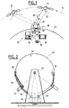
- a set of satellites 10, 12 circulates in an orbit 14 at an altitude of about 1000 to 1500 km above the surface 16 of the earth.
- Each satellite has means transmission and reception to relay communication between land users and access stations to specific services, such as databases.
- a user terminal 18 which establishes interactive communication with another user or a land station (not shown) via the satellite 12.
- the interactive character of communication is symbolized by a double arrow 20 on the path of the electromagnetic waves between the antenna 22 of the satellite 12 and antenna 24 of subscriber 18.
- the antenna 24 is, for example, arranged on the roof of a detached house. It has a focusing surface 26, for example spherical, as shown in the Figure 2, and two radiating elements 28 and 30 movable on the focal surface 26 of antenna 24.
- the radiating element 28 is controlled to follow the satellite 12 with which the user is in view, while the radiating element 30 is in a waiting position. This the latter remains pointed towards the area of appearance of the next satellite.
- the radiating element 30 replaces the element 28 used to perform the communication. The switching from element 28 to element 30 can be carried out so instant.
- the user 18 is provided with a device 32 for tracking satellites, controlling transmission and reception of signals and possibly decrypt those signals.
- This control device is connected to a microcomputer 34 or similar memory device in which are recorded information relating to the positions of the satellites, so that at all times can control the motors ensuring the movement of the radiating elements 28 and 30 so that they are pointed precisely at the satellites.
- microcomputer If a microcomputer is used, it can also be used for receive or transmit programs.
- FIG. 2 shows a more detailed example of antenna 24 with radiating elements 28 and 30.
- a fixed lens 42 is provided to receive microwave radiation over a solid angle of value sufficient to collect signals from satellites traveling in the viewing area of the user. This lens focuses the radiation received on a spherical surface on which move the radiating elements 28 and 30. This lens 42 is supported by two uprights of which only one, with reference 44, is visible in FIG. 2.
- the radiating elements 28 and 30 are movable on the spherical surface 26 focusing.
- two motors and two arms are provided for each of these elements. To simplify, we will only describe the motors and arms of the radiating element 28.
- a first motor 46 is provided. secured to a lower support 48 and the shaft of which allows an arm 50 to rotate the end of which is the second motor 52 itself driving a forearm 54 to the end of which is the radiating element 28.
- the motors 46 and 52 are controlled by information supplied by microcomputer 34 or the like.
- Each radiating element 28, 30 is associated with a transmission circuit and a reception circuit which will be described later in relation to FIG. 5.
- terminals 18 are mass-market devices, it is essential that they are compact, light in weight and minimized cost.
- the need for a small footprint and low weight is further enhanced by the fact that the devices transmission and reception are mobile and are associated in a reduced volume, that of antenna 24.
- the reception band Rx is 1 1.7 to 12.45 GHz (which can be extended to 12.55 GHz), while the Tx transmission band is from 14 to 14.3 GHz.
- the transmitting power is a few watts, of the order of 2 to 3.
- the radiating element according to the invention is of the compact type and has, for the transmission and for the reception, substantially orthogonal accesses, the phase shift of the emission and reception signals and the shape of the radiating element being such that the transmit and receive signals with different frequencies are polarized circularly in opposite directions.
- the three short-circuit, intermediate and adaptation cavities allow adjust the adaptation of the accesses in relation to the desired frequency bands.
- an access 224 is provided between the short-circuit cavity and the cavity intermediate, the other access 225 being formed between the intermediate cavity and the cavity adaptation.
- the single-band or dual-band aspects are managed by the three cavities of short-circuit, intermediate and adaptation.
- the radiative interface formed by the rectangular waveguide section polarizing 223 makes it possible to propagate two modes TE01 and TE10 orthogonal in the desired bands. Due to the rectangular section, the group speed of the TE01 modes and TE10 differs slightly which makes it possible to create a phase shift between these two modes.
- the phase quadrature between the two modes is obtained when the boundary conditions of the rectangular section 223 and its length (about ⁇ g / 4) are adequate: the antenna generates circular polarization.
- the orthogonality of accesses 224 and 225 allows isolation between accesses and the superimposed excitation of two pairs of modes TE01 and TE10 with conditions of opposite quadrature for each pair to obtain a double polarization circular.
- the cavity formed by the rectangular section 223 and the access part on the one hand and the radiative part on the other hand allows the obtaining of a quadrature condition of phase of TE01 and TE10 modes over large bandwidths.
- the stack comprising the short-circuit cavity 220, the intermediate cavity 221 and the adaptation cavity 222 constitutes a cavity which is shown circular on the Figure 7.
- This cavity can also be of substantially square shape. Its sides are then substantially perpendicular to the excitation lines 224a and 225a which constitute the access respectively 224 and 225 and therefore inclined by about 45 ° with respect to the rectangular section 223.
- the engravings may be double-sided with metallized holes. This last solution is justified in particular for applications in bands of frequencies above 6 GHz (C band).
- the radiating element is of the type planar and includes a patch or "patch" 60 (FIG. 3) having the shape of a circle truncated by parallel chamfers 62 and 64.
- a patch or "patch" 60 (FIG. 3) having the shape of a circle truncated by parallel chamfers 62 and 64.
- To this patch 60 are associated two accesses 66 and 68 in microstrip lines forming an angle of 90 °. These two accesses 66 and 68 are excited by 90 ° phase shifted signals.
- Access 66 corresponds to reception and is therefore connected, in particular, to a low noise amplifier 70
- access 68 corresponds to transmission and is therefore connected, among other things, to a power amplifier 72.
- a truncated circular flat pad 74 is provided, having an access connected to the output of the power amplifier 72 1 (transmission circuit) by means of a circulator 76.
- Access 78 is also connected to the reception channel, that is to say to a low noise amplifier 70 1 , by means of the same circulator 76.
- a planar radiating element 80 of non-truncated circular shape having two orthogonal accesses 82 and 84 connected to two terminals, respectively 86 and 88, of a hybrid coupler 90 comprising two other terminals, respectively 92 and 94.
- Terminal 92 is connected to the input of a low noise amplifier 70 2
- terminal 94 is connected to the output of power amplifier 72 2 .
- the 90 ° hybrid coupler makes it possible to transform orthogonal linear polarizations, on its terminals 92 and 94, into circular polarizations in opposite directions on its terminals 86 and 88.
- the signals have circular polarizations in opposite directions.
- the hybrid coupler 90 is preferably of the broadband type.
- one or more additional branches 96 in microstrip there is also provided in a known manner.
- FIG. 4 An embodiment planar pellet transmitting and receiving device which can preferably be used with the embodiment of Figure 3.
- two superimposed planar pads are provided, 98 and 100 respectively.
- Each of these pastilles has a shape corresponding to that shown in Figure 3, that is to say, the shape of a chamfered circle.
- dimensions of these pellets are different.
- the lower pad 98 has dimensions corresponding to a resonance in the receiving band and the patch greater than smaller dimensions corresponding to a resonance in the band the highest frequencies).
- the two tablets have a relative arrangement such that they have the same central axis (perpendicular to their planes) and that their chamfers are parallel.
- the accesses 102 are arranged under the lower patch 98. In FIG. 4 a only access is visible. These accesses are on-line micro ribbon or suspended triplate. They are connected to filter circuits and to low noise or power amplifiers by via micro ribbon or triplate lines. In the example, the filtering means and adaptation are also in line micro ribbon or triplate.
- pellets and the accesses are arranged in a cylindrical cavity 110 open upwards and presenting a bottom 112.
- This cavity 110 limits the cone of emission and reception of waves microwave so that this cone is relatively narrow, directed towards the satellite 12.
- the bottom of the cavity is connected to a channel 1 14 with an axis perpendicular to the axis 1 16 of the cylindrical cavity 1 10.
- a substrate 1 18 carrying, on the one hand, the access lines 102 and, on the other hand, filtering and adaptation circuits in micro lines tapes or triplates 120.
- the substrate also comprises, at the end of the channel 1 14 opposite to the cavity 110, active elements such as transistors 122 of amplifier (s).
- the part end of the channel 1 14 comprising the transistors 122 in planar microstrip technique is separated from the circuits 120, preferably in planar suspended three-plate technique, by through a sealing wall 124.
- the end of the channel 114 includes a terminal 128 for the signals of reception and a boom 130 for the transmission signals.
- the upper opening 132 of the cavity 110 is closed by a cover protector 134 made of plastic such as "teflon” or ABS.
- the accesses are on one of the pads, for example that of reference 98.
- planar filters and a multi-stage amplification and filtering planar filters and a multi-stage amplification and filtering.
- the attenuation, or rejection, of the filter which is the closer to the radiating element has a value which is a fraction of the attenuation necessary to eliminate the frequencies to be deleted.
- the rejection rate total necessary to eliminate the frequencies of emission (or reception) is of the order of 50 dB and the rejection of the first (or last) stage filter is only around 14 dB.
- This last value is calculated according to the compression point of the first transistor (amplifier) in reception (or of the noise factor of the last transistor, amplifier, in transmission), the power to be transmitted, or the isolation between the two ports of the source (radiating element).
- the amplification provided by the first amplification stage is preferably that which can be obtained with a very low noise transistor.
- the noise seen by the radiating element is minimized. Indeed, this noise depends mainly on the noise provided by the nearest amplifier stage and filter of this element. On the other hand, the noise brought to the radiating element by the floors more amplification and filtering only occur attenuated, because this noise is decreased in proportion to the gain of the intermediate amplification stages located between the radiating element and the noise generating filter.
- planar filters with moderate rejection can be produced from easy way, at moderate cost, because the substrates used can be of a low cost price.
- filtering using a planar micro ribbon technique requires relatively expensive alumina substrates for high rejection rates, whereas for lower rejection rates, better substrates can be used market, for example PTFE-based, as will be seen below.
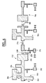
- the receiving circuit includes a first part 140 disposed between the access 142 of the patch 144 of the element radiating and one end of a cable 146.
- a second part 148 is disposed between the other end of the cable 146 and the demodulator (not shown) of the reception circuit.
- Access 142 is connected directly to the input of a first filter 150 of the type band pass for reception frequencies and band cut type for frequencies resignation. For these emission frequencies, it has a rejection characteristic relatively moderate, 14 dB. For the reception frequency, the attenuation (or loss) is low value, of the order of 0.2 dB.
- This first filter 150 is connected to the input of a first amplifier stage 152, with a single transistor in the example. This amplifier 152 shows an gain of 8 dB in the example. Note that this 8 dB gain is not the gain maximum that we could get with a transistor. But, in the example, we minimize the noise to the slight detriment of gain, as will be seen below in connection with FIG. 6.
- This first part 140 of the reception circuit also includes a second filter-amplification stage pair, namely a filter 154 whose input is connected to the output of the first amplifier 152 and a second amplifier 156 also constituted, in the example, by a single transistor.
- Filter 154 has 10 dB rejection for transmit frequencies and slight rejection, 0.2 dB, for receive frequencies.
- the amplification stage 156 has a gain of 10 dB.
- the parasitic emission signal at the output of stage 156 is less than 10 dBm.
- Cable 146 - which in the example introduces attenuation of 1.5 dB - is connected to the second filtering and amplification part 148 which includes a third filter 158-amplifier 160 pair.
- Filter 158 receives the signal supplied by cable 146 and delivers a signal to the third amplifier 160.
- the attenuation of the filter 158 for the transmit frequencies is 26.5 dB and the attenuation for receive frequencies is 1.8 dB.
- Amplification stage 160 has two transistors and its gain is 18 dB.
- stage 160 a completely filtered signal is obtained from spurious emission signals.
- This output is conventionally connected to a mixer 162 receiving a local oscillator signal at 10.75 GHz on another input. Leaving the mixer 162 is connected to the receiving demodulator via a low-pass filter 166.
- each of the filters is given to the gain of the associated amplifier so that this attenuation is sufficient to prevent delinearization, or saturation (or compression), of the amplifier transistor (s) by the spurious emission signal. It is therefore necessary that each filter is placed upstream of the associated amplifier.
- upstream we mean here that the filter should be closer to the radiating element than the amplifier of the same couple.
- the overall noise factor of the receiving circuit is essentially that of the first filter 150 and amplification stage 152.
- the coaxial cable 146 forms, in the example, a loop around the motors which may roll up or loosen depending on the movement of the arms.
- the second part 148 of the reception circuit (as well as the part corresponding to the transmission circuit) is, in the example, at the base of the antenna, that is to say near the base 48 ( Figure 2).
- the first part 142 of the reception circuit is made using so-called technology "hybrid without regulation", that is to say that the active elements such as the transistors are deposited directly on a substrate, without a housing, and that the substrate has planar conductors, for example produced by photoengraving.
- hybrid without regulation that is to say that the active elements such as the transistors are deposited directly on a substrate, without a housing, and that the substrate has planar conductors, for example produced by photoengraving.
- the part of circuit 148 located at the foot of the antenna, which is further from the radiating element, can be carried out more conventionally by integrated technology such as "Microwave monolithic integrated" circuit ", that is to say monolithic microwave integrated circuit).
- integrated technology such as "Microwave monolithic integrated” circuit ", that is to say monolithic microwave integrated circuit).
- the noise introduced by this stage 148 plays little role in the noise factor global.
- the losses of the filter 158 with a higher rejection rate (26.5 dB in the example), which avoids compression or delineation of the transistors of stage 160 are also less critical than in Part 140.
- the substrates are, for example, RO 3006 substrates or RO 4003 distributed by the Rogers Corporation. They consist of a matrix in flexible organic material such as reinforced PTFE (polytetra-fluorethylene) by micro glass fibers and in which are embedded ceramic particles allowing the dielectric constant to be increased and therefore the size of the circuits to be reduced.
- This substrate is covered, on one side, by a layer of copper which constitutes the mass, while that the other side is also covered with photogravable copper to make the circuits.
- the transmission circuit is analogous to the reception circuit.
- Access 180 emission of the patch 144 is connected to the output of a first filter 182 whose input is connected to the output of an amplification stage 184.
- the attenuation of the filter 182 is 14 dB for reception frequencies and 0.2 dB for transmission frequencies.
- the gain of amplifier 184 is 8 dB.
- the input of amplifier 184 is connected to the output of a filter 186 receiving the output signal from an amplification stage 188.
- the attenuation of the filter 186 is 10 dB for reception frequencies and 0.2 dB for transmission frequencies.
- the gain of the floor amplification 188 is 8 dB.
- the other part of the transmission circuit is also at the foot of the antenna, in the vicinity of the support 48 (FIG. 2), and includes a filter 190 connected to the cable 170 or 172 via a switch 173.
- the filter 190 receives the output signal from a stage amplifier 192 with four transistors.
- the attenuation of filter 190 is 30 dB for receive frequencies and 1.8 dB for transmit frequencies.
- the gain of amplifier 192 is 32 dB.
- the input of amplifier 192 is connected to the output of a mixer 194 by through a filter 196.
- the mixer has two inputs which, conventionally, are connected on the one hand, to the emission modulator (not shown), and on the other hand, to a local emission oscillator at 13.05 GHz.
- the advantage of the division into stages is that the top floor, directly connected to access 180, has low losses due to the low rejection rate of the filter 182 and the relatively low gain of the stage 184.
- Cable 172 is connected to the circuits associated with the second element radiant (not shown).
- the part of the transmission circuit with switch 173, filter 190, amplifier 192, filter 196 and mixer 194 is common to the two elements radiant.
- the other parts of the circuit are individual to each element radiant.
- FIG. 6 There is shown in Figure 6 a particularly embodiment simple and effective of the first part 140 of the receiving circuit.
- the first part (182, 184, 186, 188) of the transmission circuit can be carried out in a similar manner; we will not describe it therefore not in detail.
- An important characteristic of this embodiment is that of the filters 150 and 154.
- Each of these filters comprises at least one planar conducting element, formed by an etching which, in the example, is transverse to the etching 200 of current propagation. It can thus be seen that the filter 150 has a first etching elongated rectangular metal 202 perpendicular to the metal engraving 200, and ends in classic open circuit.
- the filter 150 also includes a second engraving 204 or stub in diversion on line 200. This stub 204 ends with a "pseudo short-circuit", this short-circuit being simulated by a large capacitive section 206. In the latter case, we thus avoids a connection with the ground by metallized hole (s).
- the stub 202 ending in open circuit must have a length l such that it presents at its junction with the main line 200 an open circuit for frequencies transmission and a short circuit for reception frequencies.
- This length l must be a multiple of l / 2 for the wavelengths I corresponding to reception frequencies and a multiple of l / 4 for wavelengths corresponding to the transmission frequencies.
- the length l is chosen at a value of I d / 4 , I d being a wavelength corresponding to a frequency f d equal to the difference f t - f r between two frequencies f t and f r , f t being a frequency of the transmit band and f r , a frequency of the receive band.
- m is a positive integer.
- the length l is a multiple of l / 4 for the frequencies and is a multiple of 1/2 for the receiving frequencies.
- element 202 constitutes a short circuit for the reception frequencies and an open circuit for transmission frequencies.
- the stub 204 terminated by the large capacitive section 206 simulating a short circuit at the junction 204-206, must have a length l 'chosen so that the element constitutes a short circuit for the transmission frequencies and a open circuit for reception frequencies.
- the desired result is obtained, to know the strong attenuation of the frequencies of emission and the transmission without disturbance reception frequencies.
- frequencies f r , f t and f d will be chosen, such that f r is an even multiple of f d and f t an odd multiple of f d .
- the amplifier stage 152 includes a transistor 208 as well as etchings for impedance matching and polarization of the electrodes.
- the transistor 208 is, in the example, an FHX13X transistor from the Fujitsu brand. Its grid is connected to the line 200 by means of a rectangular engraving 210. The polarizations are applied to engravings of square shapes, 212 for the grid polarization and 214 for the drain polarization.
- Stage 152 is connected to filtering stage 154 via a capacitor 216 for adaptation and decoupling between the bias voltages on the studs 212 and 214.
- the source of transistor 208 is connected to ground via a inductor 220, playing the role of a feedback and constituted by a ribbon or wire wiring or connection.
- the value of this inductor 220 is optimized so as to minimize noise. It was found that this minimization of noise can lead to a decrease in gain; but this decrease is small and does not affect performance amplification.
Landscapes
- Engineering & Computer Science (AREA)
- Radar, Positioning & Navigation (AREA)
- Remote Sensing (AREA)
- Waveguide Aerials (AREA)
- Variable-Direction Aerials And Aerial Arrays (AREA)
- Waveguide Switches, Polarizers, And Phase Shifters (AREA)
- Transceivers (AREA)
- Input Circuits Of Receivers And Coupling Of Receivers And Audio Equipment (AREA)
Applications Claiming Priority (2)
| Application Number | Priority Date | Filing Date | Title |
|---|---|---|---|
| FR9806200 | 1998-05-15 | ||
| FR9806200A FR2778802B1 (fr) | 1998-05-15 | 1998-05-15 | Dispositif d'emission et de reception d'ondes hyperfrequences polarisees circulairement |
Publications (1)
| Publication Number | Publication Date |
|---|---|
| EP0957534A1 true EP0957534A1 (de) | 1999-11-17 |
Family
ID=9526428
Family Applications (1)
| Application Number | Title | Priority Date | Filing Date |
|---|---|---|---|
| EP99401148A Withdrawn EP0957534A1 (de) | 1998-05-15 | 1999-05-10 | Vorrichtung zum Senden und Empfangen von zirkularpolarisierten Hochfrequenzwellen |
Country Status (10)
| Country | Link |
|---|---|
| US (1) | US6222493B1 (de) |
| EP (1) | EP0957534A1 (de) |
| JP (1) | JP2002516504A (de) |
| KR (1) | KR20010021841A (de) |
| CN (1) | CN1272230A (de) |
| AU (1) | AU747622B2 (de) |
| BR (1) | BR9906451A (de) |
| FR (1) | FR2778802B1 (de) |
| ID (1) | ID24491A (de) |
| WO (1) | WO1999060661A1 (de) |
Families Citing this family (17)
| Publication number | Priority date | Publication date | Assignee | Title |
|---|---|---|---|---|
| US6624787B2 (en) * | 2001-10-01 | 2003-09-23 | Raytheon Company | Slot coupled, polarized, egg-crate radiator |
| KR100845232B1 (ko) * | 2004-06-18 | 2008-07-09 | 한국전자통신연구원 | 오발(oval) 모양의 개구면을 갖는 원형 편파기 및그를 이용한 급전 혼 |
| US9172145B2 (en) | 2006-09-21 | 2015-10-27 | Raytheon Company | Transmit/receive daughter card with integral circulator |
| US7671696B1 (en) * | 2006-09-21 | 2010-03-02 | Raytheon Company | Radio frequency interconnect circuits and techniques |
| US8279131B2 (en) * | 2006-09-21 | 2012-10-02 | Raytheon Company | Panel array |
| US9019166B2 (en) | 2009-06-15 | 2015-04-28 | Raytheon Company | Active electronically scanned array (AESA) card |
| US7859835B2 (en) * | 2009-03-24 | 2010-12-28 | Allegro Microsystems, Inc. | Method and apparatus for thermal management of a radio frequency system |
| US8537552B2 (en) * | 2009-09-25 | 2013-09-17 | Raytheon Company | Heat sink interface having three-dimensional tolerance compensation |
| US8508943B2 (en) | 2009-10-16 | 2013-08-13 | Raytheon Company | Cooling active circuits |
| US8427371B2 (en) | 2010-04-09 | 2013-04-23 | Raytheon Company | RF feed network for modular active aperture electronically steered arrays |
| US8363413B2 (en) | 2010-09-13 | 2013-01-29 | Raytheon Company | Assembly to provide thermal cooling |
| US8810448B1 (en) | 2010-11-18 | 2014-08-19 | Raytheon Company | Modular architecture for scalable phased array radars |
| US8355255B2 (en) | 2010-12-22 | 2013-01-15 | Raytheon Company | Cooling of coplanar active circuits |
| US9124361B2 (en) | 2011-10-06 | 2015-09-01 | Raytheon Company | Scalable, analog monopulse network |
| US9130278B2 (en) | 2012-11-26 | 2015-09-08 | Raytheon Company | Dual linear and circularly polarized patch radiator |
| CN109361061B (zh) * | 2018-10-29 | 2021-11-02 | 湖南迈克森伟电子科技有限公司 | 天线 |
| CN109283519B (zh) * | 2018-10-29 | 2021-07-16 | 湖南迈克森伟电子科技有限公司 | 基于lfmcw测距系统 |
Citations (7)
| Publication number | Priority date | Publication date | Assignee | Title |
|---|---|---|---|---|
| US4403221A (en) * | 1981-08-10 | 1983-09-06 | Honeywell Inc. | Millimeter wave microstrip antenna |
| JPH06112724A (ja) * | 1992-09-30 | 1994-04-22 | Toshiba Corp | 2周波共用電磁結合パッチアンテナ |
| JPH06140835A (ja) * | 1991-03-14 | 1994-05-20 | Toshiba Corp | 送受共用円偏波アンテナ |
| US5434581A (en) * | 1992-11-16 | 1995-07-18 | Alcatel N.V. Societe Dite | Broadband cavity-like array antenna element and a conformal array subsystem comprising such elements |
| US5497164A (en) * | 1993-06-03 | 1996-03-05 | Alcatel N.V. | Multilayer radiating structure of variable directivity |
| JPH1022728A (ja) * | 1996-07-01 | 1998-01-23 | Toyo Commun Equip Co Ltd | 2周波共用給電結合型円偏波アンテナ |
| EP0886336A2 (de) * | 1997-06-18 | 1998-12-23 | Hughes Electronics Corporation | Flache planare, breitbandige, weitabtastende phasengesteuerte Gruppenantenne unter Verwendung von übereinanderliegenden Scheibenstrahlern |
Family Cites Families (12)
| Publication number | Priority date | Publication date | Assignee | Title |
|---|---|---|---|---|
| JPS56160103A (en) * | 1980-05-14 | 1981-12-09 | Toshiba Corp | Microstrip-type antenna |
| JPH0235514U (de) * | 1988-08-31 | 1990-03-07 | ||
| FR2648626B1 (fr) * | 1989-06-20 | 1991-08-23 | Alcatel Espace | Element rayonnant diplexant |
| US5043738A (en) * | 1990-03-15 | 1991-08-27 | Hughes Aircraft Company | Plural frequency patch antenna assembly |
| FR2668305B1 (fr) * | 1990-10-18 | 1992-12-04 | Alcatel Espace | Dispositif d'alimentation d'un element rayonnant fonctionnant en double polarisation. |
| FR2677491B1 (fr) * | 1991-06-10 | 1993-08-20 | Alcatel Espace | Antenne hyperfrequence elementaire bipolarisee. |
| US5241321A (en) * | 1992-05-15 | 1993-08-31 | Space Systems/Loral, Inc. | Dual frequency circularly polarized microwave antenna |
| JPH0652217U (ja) * | 1992-12-15 | 1994-07-15 | 松下電器産業株式会社 | デュアルビームアンテナ |
| JPH08242101A (ja) * | 1995-03-03 | 1996-09-17 | Maspro Denkoh Corp | 偏波分波器 |
| JPH0927701A (ja) * | 1995-07-11 | 1997-01-28 | Sharp Corp | 同軸導波管変換器 |
| US5812932A (en) * | 1995-11-17 | 1998-09-22 | Globalstar L.P. | Mobile satellite user information request system and methods |
| US6054953A (en) * | 1998-12-10 | 2000-04-25 | Allgon Ab | Dual band antenna |
-
1998
- 1998-05-15 FR FR9806200A patent/FR2778802B1/fr not_active Expired - Fee Related
-
1999
- 1999-05-10 KR KR1020007000405A patent/KR20010021841A/ko not_active Application Discontinuation
- 1999-05-10 BR BR9906451-0A patent/BR9906451A/pt not_active Application Discontinuation
- 1999-05-10 AU AU36106/99A patent/AU747622B2/en not_active Ceased
- 1999-05-10 CN CN99800755A patent/CN1272230A/zh active Pending
- 1999-05-10 JP JP2000550179A patent/JP2002516504A/ja active Pending
- 1999-05-10 ID IDW20000068A patent/ID24491A/id unknown
- 1999-05-10 WO PCT/FR1999/001104 patent/WO1999060661A1/fr not_active Application Discontinuation
- 1999-05-10 EP EP99401148A patent/EP0957534A1/de not_active Withdrawn
- 1999-05-10 US US09/462,516 patent/US6222493B1/en not_active Expired - Fee Related
Patent Citations (7)
| Publication number | Priority date | Publication date | Assignee | Title |
|---|---|---|---|---|
| US4403221A (en) * | 1981-08-10 | 1983-09-06 | Honeywell Inc. | Millimeter wave microstrip antenna |
| JPH06140835A (ja) * | 1991-03-14 | 1994-05-20 | Toshiba Corp | 送受共用円偏波アンテナ |
| JPH06112724A (ja) * | 1992-09-30 | 1994-04-22 | Toshiba Corp | 2周波共用電磁結合パッチアンテナ |
| US5434581A (en) * | 1992-11-16 | 1995-07-18 | Alcatel N.V. Societe Dite | Broadband cavity-like array antenna element and a conformal array subsystem comprising such elements |
| US5497164A (en) * | 1993-06-03 | 1996-03-05 | Alcatel N.V. | Multilayer radiating structure of variable directivity |
| JPH1022728A (ja) * | 1996-07-01 | 1998-01-23 | Toyo Commun Equip Co Ltd | 2周波共用給電結合型円偏波アンテナ |
| EP0886336A2 (de) * | 1997-06-18 | 1998-12-23 | Hughes Electronics Corporation | Flache planare, breitbandige, weitabtastende phasengesteuerte Gruppenantenne unter Verwendung von übereinanderliegenden Scheibenstrahlern |
Non-Patent Citations (3)
| Title |
|---|
| PATENT ABSTRACTS OF JAPAN vol. 018, no. 390 (E - 1582) 21 July 1994 (1994-07-21) * |
| PATENT ABSTRACTS OF JAPAN vol. 018, no. 447 (E - 1594) 19 August 1994 (1994-08-19) * |
| PATENT ABSTRACTS OF JAPAN vol. 098, no. 005 30 April 1998 (1998-04-30) * |
Also Published As
| Publication number | Publication date |
|---|---|
| AU3610699A (en) | 1999-12-06 |
| JP2002516504A (ja) | 2002-06-04 |
| FR2778802A1 (fr) | 1999-11-19 |
| FR2778802B1 (fr) | 2000-09-08 |
| ID24491A (id) | 2000-07-20 |
| US6222493B1 (en) | 2001-04-24 |
| BR9906451A (pt) | 2000-09-19 |
| KR20010021841A (ko) | 2001-03-15 |
| AU747622B2 (en) | 2002-05-16 |
| WO1999060661A1 (fr) | 1999-11-25 |
| CN1272230A (zh) | 2000-11-01 |
Similar Documents
| Publication | Publication Date | Title |
|---|---|---|
| EP0957534A1 (de) | Vorrichtung zum Senden und Empfangen von zirkularpolarisierten Hochfrequenzwellen | |
| EP1374340B1 (de) | Umschaltbare antenne | |
| EP0123350B1 (de) | Flache Mikrowellenantenne mit einer völlig hängenden Mikrostreifengruppe | |
| EP1074065B1 (de) | Antennensystem zur verfolgung von nichtgeostationären satelliten | |
| EP1044482A1 (de) | Sender/empfänger für elektromagnetische wellen | |
| EP2656438B1 (de) | Strahlende zelle mit zwei phasenzuständen für ein sendendes netzwerk | |
| FR2810163A1 (fr) | Perfectionnement aux antennes-sources d'emission/reception d'ondes electromagnetiques | |
| OA10623A (fr) | Système de communications interactives multifonction avec transmission et réception de signaux polarisés de façon circulaire/elliptique | |
| FR2850792A1 (fr) | Filtre compact en guide d'onde | |
| EP1074064A1 (de) | Vorrichtung zur verfolgung von nicht-geostationären satelliten | |
| EP1142063B1 (de) | Telekommunikationsgerät mit geformter gruppenantenne unter verwendung von elektronischer strahlschwenkung und dazugehöriges telekommunikations-endgerät | |
| EP1291962A1 (de) | Gruppenantennenstrahlformer für Raumfahrzeug | |
| FR2831734A1 (fr) | Dispositif pour la reception et/ou l'emission de signaux electromagnetiques a diversite de rayonnement | |
| EP0957590A1 (de) | Schaltung und Verfahren für Aussendung und Empfang von Mikrowellen | |
| EP0475162A1 (de) | Mikrowellendemodulator für digitale Funkstrecken mit QAM-Modulation | |
| FR2766995A1 (fr) | Repeteur actif pour systeme de transmission | |
| FR2818809A1 (fr) | Dispositif de filtrage d'ondes electromagnetiques | |
| FR3111480A1 (fr) | Antenne multimode, multiport et multistandard pour système de communication adaptable | |
| FR2932340A1 (fr) | Dispositif d'amplification de puissance de charge utile d'un satellite, et satellite equipe d'un tel dispositif | |
| MXPA00000471A (en) | Device for transmitting and receiving microwaves subjected to circular polarisation | |
| MXPA00000470A (en) | Circuit and method for receiving or transmitting microwaves | |
| EP1283600A1 (de) | Sende- und Empfangssystem fÜr ein Mehrband und multimode Mobiltelefon | |
| EP1056282A1 (de) | Modularer Verarbeitungsweg zur Übertragungswiederholung von einem RF analogen und digitalen Fernsehsignal und System zur Verwendung eines derartigen Verarbeitungswegs | |
| FR2953946A1 (fr) | Lentille, assemblage optique et dispositif incorporant ledit assemblage | |
| FR2903233A1 (fr) | Dispositif electronique d'antenne pour radar |
Legal Events
| Date | Code | Title | Description |
|---|---|---|---|
| PUAI | Public reference made under article 153(3) epc to a published international application that has entered the european phase |
Free format text: ORIGINAL CODE: 0009012 |
|
| AK | Designated contracting states |
Kind code of ref document: A1 Designated state(s): AT BE CH CY DE DK ES FI FR GB GR IE IT LI LU MC NL PT SE |
|
| AX | Request for extension of the european patent |
Free format text: AL;LT;LV;MK;RO;SI |
|
| 17P | Request for examination filed |
Effective date: 20000517 |
|
| AKX | Designation fees paid |
Free format text: AT BE CH CY DE DK ES FI FR GB GR IE IT LI LU MC NL PT SE |
|
| AXX | Extension fees paid |
Free format text: AL PAYMENT 20000517;LT PAYMENT 20000517;LV PAYMENT 20000517;MK PAYMENT 20000517;RO PAYMENT 20000517;SI PAYMENT 20000517 |
|
| REG | Reference to a national code |
Ref country code: HK Ref legal event code: WD Ref document number: 1022055 Country of ref document: HK |
|
| RAP1 | Party data changed (applicant data changed or rights of an application transferred) |
Owner name: ALCATEL LUCENT |
|
| 17Q | First examination report despatched |
Effective date: 20080515 |
|
| STAA | Information on the status of an ep patent application or granted ep patent |
Free format text: STATUS: THE APPLICATION IS DEEMED TO BE WITHDRAWN |
|
| 18D | Application deemed to be withdrawn |
Effective date: 20080916 |