EP0954088B1 - Schaltwandler mit mehreren geregelten Ausgängen - Google Patents
Schaltwandler mit mehreren geregelten Ausgängen Download PDFInfo
- Publication number
- EP0954088B1 EP0954088B1 EP99400487A EP99400487A EP0954088B1 EP 0954088 B1 EP0954088 B1 EP 0954088B1 EP 99400487 A EP99400487 A EP 99400487A EP 99400487 A EP99400487 A EP 99400487A EP 0954088 B1 EP0954088 B1 EP 0954088B1
- Authority
- EP
- European Patent Office
- Prior art keywords
- winding
- terminal
- output
- switching element
- mosfet
- Prior art date
- Legal status (The legal status is an assumption and is not a legal conclusion. Google has not performed a legal analysis and makes no representation as to the accuracy of the status listed.)
- Expired - Lifetime
Links
- 230000001105 regulatory effect Effects 0.000 title claims description 20
- 238000004804 winding Methods 0.000 claims description 34
- 239000003990 capacitor Substances 0.000 claims description 11
- 238000001914 filtration Methods 0.000 claims description 7
- 230000005669 field effect Effects 0.000 description 4
- 238000010586 diagram Methods 0.000 description 3
- 238000000034 method Methods 0.000 description 3
- 230000001360 synchronised effect Effects 0.000 description 3
- 230000008878 coupling Effects 0.000 description 2
- 238000010168 coupling process Methods 0.000 description 2
- 238000005859 coupling reaction Methods 0.000 description 2
- 238000012512 characterization method Methods 0.000 description 1
- 230000000295 complement effect Effects 0.000 description 1
- 230000001276 controlling effect Effects 0.000 description 1
- 238000012938 design process Methods 0.000 description 1
- 230000001939 inductive effect Effects 0.000 description 1
Images

Classifications
-
- H—ELECTRICITY
- H02—GENERATION; CONVERSION OR DISTRIBUTION OF ELECTRIC POWER
- H02M—APPARATUS FOR CONVERSION BETWEEN AC AND AC, BETWEEN AC AND DC, OR BETWEEN DC AND DC, AND FOR USE WITH MAINS OR SIMILAR POWER SUPPLY SYSTEMS; CONVERSION OF DC OR AC INPUT POWER INTO SURGE OUTPUT POWER; CONTROL OR REGULATION THEREOF
- H02M3/00—Conversion of DC power input into DC power output
- H02M3/22—Conversion of DC power input into DC power output with intermediate conversion into AC
- H02M3/24—Conversion of DC power input into DC power output with intermediate conversion into AC by static converters
- H02M3/28—Conversion of DC power input into DC power output with intermediate conversion into AC by static converters using discharge tubes with control electrode or semiconductor devices with control electrode to produce the intermediate AC
- H02M3/325—Conversion of DC power input into DC power output with intermediate conversion into AC by static converters using discharge tubes with control electrode or semiconductor devices with control electrode to produce the intermediate AC using devices of a triode or a transistor type requiring continuous application of a control signal
- H02M3/335—Conversion of DC power input into DC power output with intermediate conversion into AC by static converters using discharge tubes with control electrode or semiconductor devices with control electrode to produce the intermediate AC using devices of a triode or a transistor type requiring continuous application of a control signal using semiconductor devices only
- H02M3/33561—Conversion of DC power input into DC power output with intermediate conversion into AC by static converters using discharge tubes with control electrode or semiconductor devices with control electrode to produce the intermediate AC using devices of a triode or a transistor type requiring continuous application of a control signal using semiconductor devices only having more than one ouput with independent control
-
- G—PHYSICS
- G05—CONTROLLING; REGULATING
- G05F—SYSTEMS FOR REGULATING ELECTRIC OR MAGNETIC VARIABLES
- G05F1/00—Automatic systems in which deviations of an electric quantity from one or more predetermined values are detected at the output of the system and fed back to a device within the system to restore the detected quantity to its predetermined value or values, i.e. retroactive systems
- G05F1/10—Regulating voltage or current
- G05F1/46—Regulating voltage or current wherein the variable actually regulated by the final control device is DC
- G05F1/618—Regulating voltage or current wherein the variable actually regulated by the final control device is DC using semiconductor devices in series and in parallel with the load as final control devices
-
- H—ELECTRICITY
- H02—GENERATION; CONVERSION OR DISTRIBUTION OF ELECTRIC POWER
- H02M—APPARATUS FOR CONVERSION BETWEEN AC AND AC, BETWEEN AC AND DC, OR BETWEEN DC AND DC, AND FOR USE WITH MAINS OR SIMILAR POWER SUPPLY SYSTEMS; CONVERSION OF DC OR AC INPUT POWER INTO SURGE OUTPUT POWER; CONTROL OR REGULATION THEREOF
- H02M3/00—Conversion of DC power input into DC power output
- H02M3/22—Conversion of DC power input into DC power output with intermediate conversion into AC
- H02M3/24—Conversion of DC power input into DC power output with intermediate conversion into AC by static converters
- H02M3/28—Conversion of DC power input into DC power output with intermediate conversion into AC by static converters using discharge tubes with control electrode or semiconductor devices with control electrode to produce the intermediate AC
- H02M3/325—Conversion of DC power input into DC power output with intermediate conversion into AC by static converters using discharge tubes with control electrode or semiconductor devices with control electrode to produce the intermediate AC using devices of a triode or a transistor type requiring continuous application of a control signal
- H02M3/335—Conversion of DC power input into DC power output with intermediate conversion into AC by static converters using discharge tubes with control electrode or semiconductor devices with control electrode to produce the intermediate AC using devices of a triode or a transistor type requiring continuous application of a control signal using semiconductor devices only
- H02M3/33569—Conversion of DC power input into DC power output with intermediate conversion into AC by static converters using discharge tubes with control electrode or semiconductor devices with control electrode to produce the intermediate AC using devices of a triode or a transistor type requiring continuous application of a control signal using semiconductor devices only having several active switching elements
- H02M3/33576—Conversion of DC power input into DC power output with intermediate conversion into AC by static converters using discharge tubes with control electrode or semiconductor devices with control electrode to produce the intermediate AC using devices of a triode or a transistor type requiring continuous application of a control signal using semiconductor devices only having several active switching elements having at least one active switching element at the secondary side of an isolation transformer
- H02M3/33592—Conversion of DC power input into DC power output with intermediate conversion into AC by static converters using discharge tubes with control electrode or semiconductor devices with control electrode to produce the intermediate AC using devices of a triode or a transistor type requiring continuous application of a control signal using semiconductor devices only having several active switching elements having at least one active switching element at the secondary side of an isolation transformer having a synchronous rectifier circuit or a synchronous freewheeling circuit at the secondary side of an isolation transformer
-
- Y—GENERAL TAGGING OF NEW TECHNOLOGICAL DEVELOPMENTS; GENERAL TAGGING OF CROSS-SECTIONAL TECHNOLOGIES SPANNING OVER SEVERAL SECTIONS OF THE IPC; TECHNICAL SUBJECTS COVERED BY FORMER USPC CROSS-REFERENCE ART COLLECTIONS [XRACs] AND DIGESTS
- Y02—TECHNOLOGIES OR APPLICATIONS FOR MITIGATION OR ADAPTATION AGAINST CLIMATE CHANGE
- Y02B—CLIMATE CHANGE MITIGATION TECHNOLOGIES RELATED TO BUILDINGS, e.g. HOUSING, HOUSE APPLIANCES OR RELATED END-USER APPLICATIONS
- Y02B70/00—Technologies for an efficient end-user side electric power management and consumption
- Y02B70/10—Technologies improving the efficiency by using switched-mode power supplies [SMPS], i.e. efficient power electronics conversion e.g. power factor correction or reduction of losses in power supplies or efficient standby modes
Definitions
- the present invention relates to a switched converter with multiple outputs, of which the voltages of at least two of the outputs are regulated.
- the invention relates to a converter to convert a first voltage into at least two regulated DC voltages, where one voltage may be different from the other.
- one of the DC voltages is regulated in an indirect manner by means of an auxiliary switching element, the switching of which is controlled by means of a signal obtained from a winding of a transformer.
- a multi-output converter which has at least two regulated outputs, namely one main and one auxiliary, is known through the patent US 5,455,501 , which discloses a DC-DC converter comprising circuitry to generate the voltage of one main output and circuitry to generate the voltage of an auxiliary output. This latter voltage is generated as a function of the circuitry that generates the main output voltage.
- the circuitry that generates the main output voltage includes a switching means and an inductance means
- the circuitry of the auxiliary output includes an inductance means complementary to that of the main output circuitry.
- the inductance means is referred to the main output voltage and, consequently, depends on the presence of a minimum load on the main output.
- part of the circuitry employed in the auxiliary output ensures that the voltage of said output is regulated within a voltage range.
- the circuitry used to regulate the auxiliary output voltage requires the use of a large number of elements and, moreover, its control involves a high degree of complexity, since great precision is required in the generation of control signals to control the switching of the different switching means present in the circuitry necessary to generate the two output voltages.
- An object of the present invention is to regulate the voltage of at least one main output and one second or auxiliary output of a switched converter with multiple outputs in a simple manner which implies straightforward circuitry employing few components, whereby the regulation technique used dissipates little power.
- Another object is to obtain high performance at said second output and, consequently, the switched converter of this invention also presents a high performance. Thus, the overall cost of the multi-output switched converter is reduced.
- the switched converter comprises a transformer formed by at least a first winding and a second winding.
- the first winding is connected in series with a first switching element the duty cycle of which is controlled by a control circuit, the latter generating the switching signal for said first switching element from a sample of a first voltage present on the main output.
- the main output is formed by said second winding connected to rectifier means, for example a self-driving synchronous rectifier, and to first filtering means, including a first inductor, producing the first regulated output voltage.
- rectifier means for example a self-driving synchronous rectifier
- first filtering means including a first inductor, producing the first regulated output voltage.
- An auxiliary output is formed by a fourth switching element connected to second filtering means, including a second inductor coupled magnetically to said first inductor, producing a second regulated output voltage.
- a control circuit to control the switching of said fourth switching element by means of a control signal obtained from the voltage present on said second winding.
- Figure 1 shows a switched converter with multiple outputs according to the invention, which presents at least two regulated output voltages, corresponding a first voltage to a main output and a second voltage to an auxiliary output, respectively.
- a voltage source is connected to input nodes 11, 12 of the multi-output switched converter, in order to be converted into at least two regulated DC voltages.
- Said nodes 11, 12 are included on the primary side of a transformer T, included in said multi-output converter.
- the input node 11 is connected to a terminal 13-1 of a first winding 13 of the transformer T, for example.
- the other terminal 13-2 of the first winding 13 is connected in series with a terminal 14-1 of a first switching element 14, for example a field effect transistor MOSFET.
- a first switching element 14 for example a field effect transistor MOSFET.
- the drain 14-1 of said MOSFET 14 is connected to the terminal 13-2 of the first winding 13.
- the source 14-2 of said MOSFET is connected to the input node 12.
- a control circuit PWM for example a pulse width modulator, in accordance with a signal obtained at the main output, generates a signal to switch alternately the MOSFET 14 between turn off and turn on, that is the switching or duty cycle of said MOSFET 14 presents two parts, one with a fly-back configuration and the other with a forward configuration. This last signal is applied to the gate 14-3 of the MOSFET 14.
- the main output is formed by a second winding 15 of the transformer T, on the secondary side of said transformer T, connected to rectifier means, for example a self-driving synchronous rectifier, and first filtering means, for example a first inductance means 17 connected to a first capacitor 18.
- rectifier means for example a self-driving synchronous rectifier
- first filtering means for example a first inductance means 17 connected to a first capacitor 18.
- the current flows through the second winding 15 and a second switching element 16, also a field effect transistor MOSFET for example, and through the first inductance means 17, charging the first capacitor 18 and providing the first regulated output voltage, corresponding to the main output of the converter.
- a terminal 15-2 of the second winding 15 is connected to the drain 16-1 of the second MOSFET 16, the source 16-2 is connected to the terminal 17-1 of the first inductor 17, and its gate 16-3 is connected to the terminal 15-1 of the second winding 15.
- the second MOSFET 16 together with a third switching element 19, as well as a field effect transistor MOSFET, form the self-driving synchronous rectifier, whereby the rectifier arm is constituted by the second MOSFET 16 and the free wheeling arm is constituted by the third MOSFET 19.
- drain 19-1 of the third MOSFET 19 is connected to the terminal 15-1 of the second winding 15, the gate 19-3 to the other terminal 15-2 of the same winding 15 and the source 19-2 to the terminal 17-1 of the first inductance 17.
- the switched multi-output converter of the invention presents a forward topology with the outputs isolated.
- the values of the first inductor 17 and of the first capacitor 18, which form the first filtering means, are chosen by the designer in order to obtain the value of voltage required at the main output and, in addition, for filtering said output voltage.
- the auxiliary output includes a second inductor 20 magnetically coupled to the first inductor 17, for example on the same core, in such a way that a terminal 20-2 is connected to a terminal of a second capacitor 21 to form an output node 24-1 of the auxiliary output.
- the drain 22-1 of the fourth MOSFET 22 is connected to the terminal 20-1 of said inductor 20 and its source 22-2 is connected to a terminal of the second capacitor 21 to form the other output node 24-2.
- said source 22-2 is connected to the terminal 15-1 of the second winding 15.
- the second output voltage at the auxiliary output is regulated by means of the coupling of the first inductor 17 and the second inductor 20, obtaining the regulated output voltage across the output nodes 24-1, 24-2.
- the power supplied through the auxiliary output is less than the power supplied through the main output.
- the switching to turn off and to turn on the fourth MOSFET 22 is controlled by means of a control signal generated by a control circuit 23. Said control signal is applied to the gate 22-3 of the fourth MOSFET 22.
- the control circuit 23 obtains the control signal from the alternating voltage waveform present on the second winding 15.
- Figure 2 shows a preferred embodiment of the control circuit 23, which includes a third capacitor 25 such that one of its terminals is connected to the terminal 15-2 of the second winding and its other terminal is connected to the gate 22-3 of the fourth MOSFET 22.
- the cathode of a Zener diode 27 is connected to the terminal 22-3 of the fourth MOSFET 22, and the anode of said Zener diode 27 is connected to the terminal 22-2 of said MOSFET 22. It also includes a first resistance 26 connected across the terminals 22-3 and 22-2 of said MOSFET 22.
- the third capacitor 25 When the second MOSFET 16 turns on, the third capacitor 25 is charged, the fourth MOSFET 22 being turn off.
- the capacitor 25 discharges through the first resistance 26, corresponding to the period of conduction of the fourth MOSFET 22 since the control signal is applied at its gate 22-3, this period coinciding with that of conduction of the third MOSFET 19.
- the second capacitor 21 supplies the voltage to the output nodes 24-1, 24-2.
- the Zener diode 27 protects the fourth MOSFET 22 against voltage peaks, for example surge voltages.
- the multi-output current converter presents at least two outputs with their voltages regulated, the main output having a forward configuration and its output voltage being regulated by controlling the switching of the first MOSFET 14, and the auxiliary output having a fly-back configuration, its output voltage being regulated by means of the coupling between the first inductor 17 and the second inductor 20.
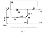
- control circuit 23 can obtain the control signal from the alternating voltage waveform present on a third winding 31, this implementation being shown in figure 3 . Therefore, the two outputs are isolated.
- FIG. 3 shows another embodiment of the control circuit 23.
- the control signal being applied to the terminal 22-3 of the fourth MOSFET 22, which comes into conduction.
- the auxiliary output has its output voltage regulated.
Landscapes
- Engineering & Computer Science (AREA)
- Power Engineering (AREA)
- Physics & Mathematics (AREA)
- Electromagnetism (AREA)
- General Physics & Mathematics (AREA)
- Radar, Positioning & Navigation (AREA)
- Automation & Control Theory (AREA)
- Dc-Dc Converters (AREA)
Claims (4)
- Schaltwandler mit mehreren geregelten Ausgängen, umfassend:einen Transformator (T) mit zumindest einer ersten Wicklung (13) und einer zweiten (15) Wicklung, wobei die erste Wicklung (13) mit einem ersten Schaltelement (14) verbunden ist, dessen Einschaltdauer von einem Steuerkreis (PWM) gesteuert ist, und wobei die zweite Wicklung (15) mit Mitteln zum Stromrichten (16, 19) und mit einem ersten Mittel zum Filtern, umfassend eine erste Induktanz (17) verbunden ist, um eine erste geregelte Ausgangsspannung zu erzeugen,dadurch gekennzeichnet, daß
der Schaltwandler ein viertes Schaltelement (22) umfaßt, welches mit einem zweiten Mittel zum Filtern, umfassend eine zweite Induktanz (20), welche mit der ersten Induktanz (17) magnetisch verbunden ist, um eine zweite geregelte Ausgangsspannung zu erzeugen, und daß ein Steuerkreis (23) das Schalten des vierten Schaltelements (22) mittels eines Steuersignals steuert, welches von einer an der zweiten Wicklung (15) vorhandenen Spannung erhalten wird. - Schaltwandler nach Anspruch 1,
dadurch gekennzeichnet, daß
der Steuerkreis (23) einen dritten Kondensator (25) umfaßt, welcher zwischen einem Anschluß (15-2) der zweiten Wicklung (15) und dem Steueranschluß (22-3) des vierten Schaltelements (22) verbunden ist, wobei die Kathode einer Zener-Diode (27) mit dem Steueranschluß (22-3) verbunden ist und wobei die Anode der Zener-Diode (27) mit einem anderen Anschluß (22-2) des vierten Schaltelements (22) verbunden ist und parallel zur Zener-Diode (27) ein erster Widerstand (26) geschaltet ist. - Schaltwandler nach Anspruch 1,
dadurch gekennzeichnet, daß
der Transformator (T) eine dritte Wicklung (31) umfaßt und daß
das Steuersignal von einer Spannung, welche an der dritten Wicklung (31) statt der zweiten Wicklung (15) vorhanden ist, erhalten wird. - Schaltwandler nach Anspruch 3,
dadurch gekennzeichnet, daß
der Steuerkreis (23) eine Diode umfaßt, deren Anode mit einem Anschluß (31-2) der dritten Wicklung (31) verbunden ist und deren Kathode über einen zweiten Widerstand (34) mit dem Steueranschluß (22-3) des vierten Schaltelements (22) verbunden ist, wobei der Steueranschluß (33-3) eines fünften Schaltelements (33) über einen fünften Widerstand (35) mit dem Anschluß (31-2) der dritten Wicklung (31) verbunden ist und ein anderer Anschluß (33-2) des fünften Schaltelements (33) mit dem anderen Anschluß (31-1) der dritten Wicklung (31) verbunden ist.
Applications Claiming Priority (2)
| Application Number | Priority Date | Filing Date | Title |
|---|---|---|---|
| ES9800671 | 1998-03-30 | ||
| ES009800671A ES2143406B1 (es) | 1998-03-30 | 1998-03-30 | Convertidor conmutado con multiples salidas reguladoras. |
Publications (2)
| Publication Number | Publication Date |
|---|---|
| EP0954088A1 EP0954088A1 (de) | 1999-11-03 |
| EP0954088B1 true EP0954088B1 (de) | 2009-12-09 |
Family
ID=8303275
Family Applications (1)
| Application Number | Title | Priority Date | Filing Date |
|---|---|---|---|
| EP99400487A Expired - Lifetime EP0954088B1 (de) | 1998-03-30 | 1999-03-01 | Schaltwandler mit mehreren geregelten Ausgängen |
Country Status (5)
| Country | Link |
|---|---|
| US (1) | US6128203A (de) |
| EP (1) | EP0954088B1 (de) |
| CA (1) | CA2265003A1 (de) |
| DE (1) | DE69941755D1 (de) |
| ES (1) | ES2143406B1 (de) |
Families Citing this family (17)
| Publication number | Priority date | Publication date | Assignee | Title |
|---|---|---|---|---|
| US7269034B2 (en) | 1997-01-24 | 2007-09-11 | Synqor, Inc. | High efficiency power converter |
| JP2002514378A (ja) | 1997-01-24 | 2002-05-14 | シンクォール・インコーポレーテッド | 高効率電力変換装置 |
| FI110972B (fi) * | 1999-03-10 | 2003-04-30 | Abb Industry Oy | Stabiloitu hilaohjain |
| CN1101989C (zh) * | 1999-12-27 | 2003-02-19 | 艾默生网络能源有限公司 | Dc/dc变换器的自驱动电路 |
| CN1108011C (zh) * | 1999-12-30 | 2003-05-07 | 艾默生网络能源有限公司 | Dc/dc变换器的自驱动电路 |
| FR2835662B1 (fr) * | 2002-02-07 | 2005-08-19 | Cit Alcatel | Circuit secondaire de convertisseur comportant au moins une sortie auxiliaire |
| FR2863788A1 (fr) * | 2003-12-11 | 2005-06-17 | Invensys Appliance Controls Sa | Alimentation electrique a decoupage avec isolation |
| CN100438295C (zh) * | 2005-06-01 | 2008-11-26 | 台达电子工业股份有限公司 | 多重输出直流-直流转换器 |
| FR2902581B1 (fr) * | 2006-06-14 | 2008-10-24 | Power Supply Systems Holdings | Convertisseur continu-continu a sorties multiples |
| TWI344586B (en) * | 2008-01-07 | 2011-07-01 | Lite On Technology Corp | Power supply device capable of rectifying output voltage |
| CN101483390B (zh) * | 2008-01-07 | 2011-07-06 | 光宝科技股份有限公司 | 可调整输出电压的电源供应装置 |
| US8310847B2 (en) * | 2009-08-04 | 2012-11-13 | Niko Semiconductor Co., Ltd. | Secondary side post regulator of flyback power converter with multiple outputs |
| US10199950B1 (en) | 2013-07-02 | 2019-02-05 | Vlt, Inc. | Power distribution architecture with series-connected bus converter |
| US10116224B1 (en) * | 2017-06-14 | 2018-10-30 | Northrop Grumman Systems Corporation | Switching power converter circuit |
| EP4220925A1 (de) * | 2022-01-26 | 2023-08-02 | Tridonic GmbH & Co. KG | Schaltwandler |
| TWI888864B (zh) * | 2023-07-12 | 2025-07-01 | 康舒科技股份有限公司 | 具有環場效電晶體的電源供應器 |
| CN119891708B (zh) * | 2025-03-27 | 2025-05-27 | 北京怀柔实验室 | 功率半导体器件的驱动取能系统及驱动取能方法 |
Citations (1)
| Publication number | Priority date | Publication date | Assignee | Title |
|---|---|---|---|---|
| EP0605752A2 (de) * | 1993-01-05 | 1994-07-13 | Yokogawa Electric Corporation | Schaltnetzteil |
Family Cites Families (8)
| Publication number | Priority date | Publication date | Assignee | Title |
|---|---|---|---|---|
| DE3843183A1 (de) | 1988-12-22 | 1990-07-05 | Philips Patentverwaltung | Getaktete stromversorgungseinrichtung |
| JP2682202B2 (ja) * | 1990-06-08 | 1997-11-26 | 日本電気株式会社 | 電界効果トランジスタを用いた整流回路 |
| US5162663A (en) * | 1990-09-28 | 1992-11-10 | Ncr Corporation | Selective output disconnect for a single transformer converter |
| US5479087A (en) * | 1992-10-02 | 1995-12-26 | Compaq Computer Corp. | Synchronized switch tapped coupled inductor regulation circuit |
| US5400239A (en) * | 1992-12-11 | 1995-03-21 | Northern Telecom Limited | Power converter with plural regulated outputs |
| US5455501A (en) | 1994-03-24 | 1995-10-03 | Intel Corporation | Multiple output DC-DC converter with different ranges of output assurance and capable of tolerating load transients |
| DE4441492A1 (de) * | 1994-11-22 | 1996-05-23 | Abb Research Ltd | Potentialtrennende Treiberschaltung zur Ansteuerung spannungsgesteuerter Halbleiterventile |
| JP3259128B2 (ja) * | 1995-09-26 | 2002-02-25 | 富士通電装株式会社 | 同期整流回路 |
-
1998
- 1998-03-30 ES ES009800671A patent/ES2143406B1/es not_active Expired - Fee Related
-
1999
- 1999-03-01 DE DE69941755T patent/DE69941755D1/de not_active Expired - Lifetime
- 1999-03-01 EP EP99400487A patent/EP0954088B1/de not_active Expired - Lifetime
- 1999-03-03 US US09/261,174 patent/US6128203A/en not_active Expired - Lifetime
- 1999-03-29 CA CA002265003A patent/CA2265003A1/en not_active Abandoned
Patent Citations (1)
| Publication number | Priority date | Publication date | Assignee | Title |
|---|---|---|---|---|
| EP0605752A2 (de) * | 1993-01-05 | 1994-07-13 | Yokogawa Electric Corporation | Schaltnetzteil |
Also Published As
| Publication number | Publication date |
|---|---|
| EP0954088A1 (de) | 1999-11-03 |
| US6128203A (en) | 2000-10-03 |
| ES2143406B1 (es) | 2000-12-16 |
| ES2143406A1 (es) | 2000-05-01 |
| CA2265003A1 (en) | 1999-09-30 |
| DE69941755D1 (de) | 2010-01-21 |
Similar Documents
| Publication | Publication Date | Title |
|---|---|---|
| EP0954088B1 (de) | Schaltwandler mit mehreren geregelten Ausgängen | |
| US5654881A (en) | Extended range DC-DC power converter circuit | |
| EP0428377B1 (de) | Gleichspannungs-Schaltwandler-Schaltkreis | |
| AU705922B2 (en) | DC to DC transformer-based converter with push pull electronic switching | |
| US6191957B1 (en) | Extended range boost converter circuit | |
| US5140510A (en) | Constant frequency power converter | |
| US5541828A (en) | Multiple output converter with continuous power transfer to an output and with multiple output regulation | |
| US5132888A (en) | Interleaved bridge converter | |
| EP0508664B1 (de) | Gleichspannungswandler | |
| US6570268B1 (en) | Synchronous rectifier drive circuit and power supply including same | |
| WO2018025452A1 (ja) | 直流電圧変換回路 | |
| US5977753A (en) | Buck regulator with plural outputs | |
| CN115864858A (zh) | 一种辅助电源、电源系统和电子装置 | |
| US20030021130A1 (en) | Switching power converter apparatus and methods using switching cycle with energy holding state | |
| EP1763124A2 (de) | Gleichstromwandler | |
| EP0720278B1 (de) | Leistungsbegrenzender Regler | |
| US6288918B1 (en) | Switched power converter with hold-up time and harmonics reduction | |
| US6229717B1 (en) | Switched power supply converter operable in a natural zero-voltage switching mode | |
| JP2002315331A (ja) | Dc/dcコンバータを具えた電源装置 | |
| JPH06141536A (ja) | Dc/dcコンバータを含む低損失電源供給装置 | |
| US8324872B2 (en) | Voltage regulator with coupled inductors having high coefficient of coupling | |
| CN114696602A (zh) | 功率变换电路 | |
| CN113273067A (zh) | 具有耦合降压转换处理级的开关电源 | |
| JP4144715B2 (ja) | Dcーdcコンバータ | |
| EP3537253A1 (de) | Kaskadierter spannungswandler mit zwischenstufiger magnetischer leistungskopplung |
Legal Events
| Date | Code | Title | Description |
|---|---|---|---|
| PUAI | Public reference made under article 153(3) epc to a published international application that has entered the european phase |
Free format text: ORIGINAL CODE: 0009012 |
|
| AK | Designated contracting states |
Kind code of ref document: A1 Designated state(s): CH DE FR GB IE IT LI SE |
|
| AX | Request for extension of the european patent |
Free format text: AL;LT;LV;MK;RO;SI |
|
| 17P | Request for examination filed |
Effective date: 20000408 |
|
| AKX | Designation fees paid |
Free format text: CH DE FR GB IE IT LI SE |
|
| RAP1 | Party data changed (applicant data changed or rights of an application transferred) |
Owner name: ALCATEL LUCENT |
|
| 17Q | First examination report despatched |
Effective date: 20071128 |
|
| GRAP | Despatch of communication of intention to grant a patent |
Free format text: ORIGINAL CODE: EPIDOSNIGR1 |
|
| RAP1 | Party data changed (applicant data changed or rights of an application transferred) |
Owner name: POWER SUPPLY SYSTEMS HOLDING ( THE NETHERLANDS) B. |
|
| GRAS | Grant fee paid |
Free format text: ORIGINAL CODE: EPIDOSNIGR3 |
|
| GRAA | (expected) grant |
Free format text: ORIGINAL CODE: 0009210 |
|
| RAP1 | Party data changed (applicant data changed or rights of an application transferred) |
Owner name: AEG POWER SOLUTIONS B.V. |
|
| AK | Designated contracting states |
Kind code of ref document: B1 Designated state(s): CH DE FR GB IE IT LI SE |
|
| REG | Reference to a national code |
Ref country code: GB Ref legal event code: FG4D |
|
| REG | Reference to a national code |
Ref country code: CH Ref legal event code: EP |
|
| REG | Reference to a national code |
Ref country code: IE Ref legal event code: FG4D |
|
| REF | Corresponds to: |
Ref document number: 69941755 Country of ref document: DE Date of ref document: 20100121 Kind code of ref document: P |
|
| PG25 | Lapsed in a contracting state [announced via postgrant information from national office to epo] |
Ref country code: SE Free format text: LAPSE BECAUSE OF FAILURE TO SUBMIT A TRANSLATION OF THE DESCRIPTION OR TO PAY THE FEE WITHIN THE PRESCRIBED TIME-LIMIT Effective date: 20091209 |
|
| PLBE | No opposition filed within time limit |
Free format text: ORIGINAL CODE: 0009261 |
|
| STAA | Information on the status of an ep patent application or granted ep patent |
Free format text: STATUS: NO OPPOSITION FILED WITHIN TIME LIMIT |
|
| REG | Reference to a national code |
Ref country code: CH Ref legal event code: PL |
|
| 26N | No opposition filed |
Effective date: 20100910 |
|
| PG25 | Lapsed in a contracting state [announced via postgrant information from national office to epo] |
Ref country code: IE Free format text: LAPSE BECAUSE OF NON-PAYMENT OF DUE FEES Effective date: 20100301 |
|
| PG25 | Lapsed in a contracting state [announced via postgrant information from national office to epo] |
Ref country code: LI Free format text: LAPSE BECAUSE OF NON-PAYMENT OF DUE FEES Effective date: 20100331 Ref country code: CH Free format text: LAPSE BECAUSE OF NON-PAYMENT OF DUE FEES Effective date: 20100331 |
|
| PGFP | Annual fee paid to national office [announced via postgrant information from national office to epo] |
Ref country code: DE Payment date: 20120315 Year of fee payment: 14 |
|
| PGFP | Annual fee paid to national office [announced via postgrant information from national office to epo] |
Ref country code: IT Payment date: 20120326 Year of fee payment: 14 Ref country code: GB Payment date: 20120320 Year of fee payment: 14 |
|
| PGFP | Annual fee paid to national office [announced via postgrant information from national office to epo] |
Ref country code: FR Payment date: 20120416 Year of fee payment: 14 |
|
| GBPC | Gb: european patent ceased through non-payment of renewal fee |
Effective date: 20130301 |
|
| REG | Reference to a national code |
Ref country code: FR Ref legal event code: ST Effective date: 20131129 |
|
| REG | Reference to a national code |
Ref country code: DE Ref legal event code: R119 Ref document number: 69941755 Country of ref document: DE Effective date: 20131001 |
|
| PG25 | Lapsed in a contracting state [announced via postgrant information from national office to epo] |
Ref country code: FR Free format text: LAPSE BECAUSE OF NON-PAYMENT OF DUE FEES Effective date: 20130402 Ref country code: DE Free format text: LAPSE BECAUSE OF NON-PAYMENT OF DUE FEES Effective date: 20131001 Ref country code: GB Free format text: LAPSE BECAUSE OF NON-PAYMENT OF DUE FEES Effective date: 20130301 |
|
| PG25 | Lapsed in a contracting state [announced via postgrant information from national office to epo] |
Ref country code: IT Free format text: LAPSE BECAUSE OF NON-PAYMENT OF DUE FEES Effective date: 20130301 |