EP0943178B1 - Short circuit protection for a semiconductor switch - Google Patents
Short circuit protection for a semiconductor switch Download PDFInfo
- Publication number
- EP0943178B1 EP0943178B1 EP98925659A EP98925659A EP0943178B1 EP 0943178 B1 EP0943178 B1 EP 0943178B1 EP 98925659 A EP98925659 A EP 98925659A EP 98925659 A EP98925659 A EP 98925659A EP 0943178 B1 EP0943178 B1 EP 0943178B1
- Authority
- EP
- European Patent Office
- Prior art keywords
- field effect
- voltage
- effect transistor
- source
- fet
- Prior art date
- Legal status (The legal status is an assumption and is not a legal conclusion. Google has not performed a legal analysis and makes no representation as to the accuracy of the status listed.)
- Expired - Lifetime
Links
- 239000004065 semiconductor Substances 0.000 title description 6
- 230000005669 field effect Effects 0.000 claims abstract description 38
- 238000005259 measurement Methods 0.000 claims abstract description 14
- 230000000694 effects Effects 0.000 claims abstract description 13
- 238000000034 method Methods 0.000 claims description 8
- 230000007423 decrease Effects 0.000 description 10
- 239000008186 active pharmaceutical agent Substances 0.000 description 6
- 230000006378 damage Effects 0.000 description 4
- 238000004519 manufacturing process Methods 0.000 description 2
- 239000013641 positive control Substances 0.000 description 2
- 238000010586 diagram Methods 0.000 description 1
- 238000013021 overheating Methods 0.000 description 1
Images

Classifications
-
- H—ELECTRICITY
- H03—ELECTRONIC CIRCUITRY
- H03K—PULSE TECHNIQUE
- H03K17/00—Electronic switching or gating, i.e. not by contact-making and –breaking
- H03K17/08—Modifications for protecting switching circuit against overcurrent or overvoltage
- H03K17/082—Modifications for protecting switching circuit against overcurrent or overvoltage by feedback from the output to the control circuit
- H03K17/0822—Modifications for protecting switching circuit against overcurrent or overvoltage by feedback from the output to the control circuit in field-effect transistor switches
-
- H—ELECTRICITY
- H03—ELECTRONIC CIRCUITRY
- H03K—PULSE TECHNIQUE
- H03K17/00—Electronic switching or gating, i.e. not by contact-making and –breaking
- H03K17/51—Electronic switching or gating, i.e. not by contact-making and –breaking characterised by the components used
- H03K17/56—Electronic switching or gating, i.e. not by contact-making and –breaking characterised by the components used by the use, as active elements, of semiconductor devices
- H03K17/687—Electronic switching or gating, i.e. not by contact-making and –breaking characterised by the components used by the use, as active elements, of semiconductor devices the devices being field-effect transistors
- H03K17/6871—Electronic switching or gating, i.e. not by contact-making and –breaking characterised by the components used by the use, as active elements, of semiconductor devices the devices being field-effect transistors the output circuit comprising more than one controlled field-effect transistor
- H03K17/6874—Electronic switching or gating, i.e. not by contact-making and –breaking characterised by the components used by the use, as active elements, of semiconductor devices the devices being field-effect transistors the output circuit comprising more than one controlled field-effect transistor in a symmetrical configuration
-
- H—ELECTRICITY
- H03—ELECTRONIC CIRCUITRY
- H03K—PULSE TECHNIQUE
- H03K2217/00—Indexing scheme related to electronic switching or gating, i.e. not by contact-making or -breaking covered by H03K17/00
- H03K2217/0027—Measuring means of, e.g. currents through or voltages across the switch
Definitions
- the present invention relates generally to a method of protecting semiconductor switches against destruction or damage caused by a short circuit.
- the present invention relates especially to a protection in semiconductor switches with a limited switching speed.
- Semiconductor switches are commonly used in electrical control applications, because their electrical control can be easily arranged and they contain no moving, wear-prone parts. Thyristors and different kinds of transistors, such as bipolar transistors, FETs (field effect transistors) and IGBT transistors (isolated gate bipolar transistors) are commonly used as switching components.
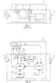
- FIG. 1 is a simplified illustration of a known stepless power control 11 for changing the amount of electrical power fed from an AC voltage source 12 to a resistive load 13.
- the power control of figure 1 is suitable for use as e.g. a dimmer of a mains voltage lighting fixture.
- the power control 11 comprises a field effect transistor unit, which in this case consists of two FETs 14 and 15 connected in series so that the drain of the first FET is connected to an AC current source 12 via a low-resistance current measurement resistor 16, the drain of the second FET is connected to the load 13 and the sources of FETs 14 and 15 are connected to each other.
- the gates of the FETs 14 and 15 are connected to control circuit 17 which regularly emits connecting pulses for connecting the FETs to conducting state for the desired time.
- the mean value of the electric power fed to the load 13 depends on the cycle ratio used in the circuit, i.e. the ratio of the duration of the conducting state of the FETs to the duration of the connecting cycle.
- the duration of the conducting state of the FET is called switch-on period.
- a previously known short circuit protection control requires a current measurement resistor rated for a relatively large throughput current.
- a resistive component connected in series causes a power loss the magnitude of which is proportional to the resistance of the component.
- the power loss can be minimized by using a current measurement resistor of very small resistance, but this in turn requires stricter tolerances for the measurement circuit measuring the voltage over the current measurement resistor. Strict tolerances increase manufacturing costs.
- the purpose of the invention is to disclose a short circuit protection for a power control with small manufacturing costs and reliable and fast operation in case the semiconductor switch is switched to conducting state when there is voltage over the switch.
- the aim of the invention is reached by measuring the gate voltage change of the FET acting as the switching element during switching operation and comparing it to the drain-source voltage measured over the FET and by either allowing or disabling the switching of the FET to conducting state on the basis of the result of the measurement.
- a characterizing feature of a power control according to the invention comprising a field effect transistor is that it comprises means for measuring the change of the gate potential of the field effect transistor in relation to the voltage over the FET between the source and the drain and means for either allowing or disabling the switching of the FET to conducting state on the basis of the result of the measurement.
- the present invention also relates to a method of protecting a power control from the negative effects of an excessive throughput current.
- a characterizing feature of the method according to the invention is that in the method the change of the FET gate voltage potential is measured in relation to the voltage over the field effect transistor between the source and the drain at the start of the gate control pulse of the field effect transistor and that the switching of the FET to conducting state is either allowed or disabled on the basis of the result of the gate voltage change measurement.
- the gate voltage of the FET is measured and compared with a reference voltage higher than the value where the increase of the gate voltage temporarily stops due to Miller effect. If the gate voltage exceeds the reference voltage when the voltage between the drain and the source is high, there is a short circuit. In this case, gate voltage input to the FET will be cut.
- the present invention is especially suitable for use in applications in which it is desirable to switch the FET controlling the alternating voltage throughput to conducting state in other phases than during the zero point of the alternating voltage.
- the circuit according to the invention can be manufactured using inexpensive low voltage components.
- the power control 20 of figure 2 comprises FETs 21a and 21b, a control circuit 22, a voltage measurement circuit 23 for the voltage between the drain and the source, a gate voltage measurement circuit 24, a comparison means 24 and a block 26 for either allowing or disabling gate voltage pulse input to the gate of the FETs 21a and 21b depending on the result of the comparison means 25.
- the power control controls the amount of electrical power fed from AC voltage source 12 to load 13.
- the voltage curves illustrated in figure 3 will greatly ease the understanding of the operating principle of a circuit according to figure 2.
- the voltage curves of figure 3 are purely qualitative, so the vertical voltage scale of the figure is irrelevant as far as the invention is concerned.
- the horizontal axis is the time axis, but its scale is irrelevant to the invention as well.
- the scale can be described by stating the fact that in order to reduce RF interference the aim is not to switch the semiconductor switches of the power control to conducting state as fast as possible, but the aim is to maintain the switching times in the range of some tens of microseconds.
- the curve 31 illustrates the gate voltage U G of the switching FET 21a or 21b as a function of time when the FET is switched to conducting state and there is no short circuit in the load 13.
- the curve 32 illustrates the gate voltage U G of a FET as a function of time when the FET is switched to conducting state and there is a short circuit in the load 13.
- the curve 33 illustrates the voltage between the drain and source of the FET, when the FET is switched to conducting state and there is no short circuit in the load 13.
- the curve 34 illustrates the voltage between the drain and source of the FET, when the FET is switched to conducting state and there is a short circuit in the load 13.
- the gate voltage U G starts to increase.
- curves 31 and 33 are compared to each other, it can be seen that initially the gate voltage U G increases rapidly, but the increase evens out for the duration of the interval t 1 while the voltage U DS between the drain and source decreases rapidly during the interval t 1 .
- the behaviour of the voltages is due to the Miller effect, known as such, which in turn is caused by the non-ideal conditions of the FET, especially the internal capacitances of the FET.
- the Miller effect causes the gate voltage U G to exceeds the reference voltage U ref only after a time corresponding to the interval t 1 later than were the case without the momentary evening out caused by the Miller effect.
- the voltage U DS between the drain and the source of the FET does not decrease noticeably even though the FET is switched to conducting state, but remains nearly constant as described by the curve 34, because the mains network feeding electrical power to the circuit is a rigid source.
- the current through both the FET and the load increases rapidly.
- the Miller effect does not reduce the increase of the gate voltage U G , but it rises to its peak value as described by curve 33.
- the gate voltage U G exceeds the reference voltage U ref noticeably sooner than in normal situation with a relatively high resistance of the load 13.
- the comparison means 25 compares on the other hand the gate voltage U G to the reference voltage U ref arid on the other hand monitors the value of the voltage U DS between the drain and source of the switching FET.
- the operation of the comparison means is illustrated in the following table. U G U DS Connecting the gate voltage pulse ⁇ U ref large allowed >U ref large disabled X small allowed
- the X at the lower left corner of the table indicates that in this case the value of the gate voltage U G is irrelevant.
- a detailed exemplary embodiment of the invention disclosed later specifies a way of defining the values "large” and "small” of the voltage U DS .
- the values in the right-hand column define whether the comparison means 25 instructs the block 26 either to allow or disable the sending of the gate voltage pulse to the FET. This means that if the gate voltage U G is significantly higher than the reference voltage without a significant decrease in the voltage U DS between the drain and source, the comparison means interprets this as a short circuit in the load 13, and so activates block 26 to disable the positive voltage produced by block 22 from reaching the gate of the FET 21a or 21b.
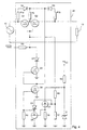
- FIG 4 illustrates an embodiment of the invention as a circuit diagram.
- the power control 40 comprises in this case as well two FETs Q1 and Q2 connected in series along the current path from the AC power source 12 to the load 13 in the same way as in the previously known solution illustrated in figure 1.
- the control voltage pulses are fed to the gates of the FETs Q1 and Q2 from the control circuit (not shown for clearness) via resistor R3.
- the control circuit can be a previously known control circuit.
- a first voltage dividing circuit comprising two resistors R1a and R2 and a diode D4 with the diode D4 connected between the resistors so that its anode is connected to the resistor R1a and its cathode is connected to the resistor R2 is connected in parallel with the first FET Q1, i.e. between the drain and the source of the FET.
- the point between the cathode of the diode D4 and the resistor R2 is connected to the gate of the FET Q3 and to the drain of the FET Q4.
- the resistors Rlb and R2 and the diode D5 form correspondingly a second voltage dividing circuit over the FET Q2.
- the gates of the FETs Q1 and Q2 are connected via a forward diode D1 to the drain of the FET Q3 and the source of the FET Q3 is connected to earth potential.
- the point between the resistors R6 and R7 is connected to the base of a bipolar pnp transistor Q5, which is further connected to the emitter of bipolar pnp transistor Q6 via a forward diode.
- the collector of the transistor Q5 is connected to the base of the transistor Q6 and further to earth potential via shunting resistor R8.
- the collector of the transistor Q6 is connected to earth potential.
- the point between the cathode of the diode D3 and the emitter of the transistor Q6 is connected to the gate of the FET Q4 and further to earth potential via shunting resistor R9.
- the circuit formed by the transistors Q5 and Q6 and the passive components connected thereto is a comparison means for producing a positive voltage signal to the gate of the FET Q4 only when the emitter voltage of the transistor Q5 is higher than the gate voltage of the
- the circuit illustrated in figure 4 operates as follows: If there currently is a positive half-cycle in the alternating voltage 12, the first voltage dividing unit formed by the resistors R1a and R2 and the diode D4 forms a certain positive voltage, proportional to the momentary value of the alternating voltage, for trying to switch the FET Q3 to conducting state. But if the voltage between the gate of the FET Q1 and the earth potential is smaller than the reference voltage formed from input voltage +U cc (for example +10 V) by means of the resistor R5 and the zener diode Z1, the transistors Q5 and Q6 are in non-conducting state.
- the current flowing from the reference voltage to earth potential via the diode D3 and the resistor R9 forms a positive voltage to the gate of the FET Q4 for keeping the FET Q4 in conducting state, whereby the voltage formed by the first voltage dividing circuit R1a, D4 and R2 flows to earth potential via FET Q4 and does not switch the FET Q3 to conducting state.
- the voltage UDS between the drain and source of the FET Q1 will decrease to a low level before the gate voltage U G of the FET Q1 (and the part thereof produced by the third voltage dividing circuit R6, R7) starts to increase again.
- the base voltage of the transistor Q5 increases so as to exceed the reference voltage formed from the input voltage +U cc by means of the resistor R5 and the zener diode Z1
- the transistors Q5 and Q6 are switched to conducting state, whereby the gate voltage of the FET Q4 decreases to near zero and the FET Q4 is switched to non-conducting state.
- the FET Q3 could be switched to conducting state, if the voltage produced by the first voltage dividing circuit R1, R2 were large enough, but as this voltage has already had the time to decrease when the FET Q1 is switched to conducting state, this will not happen.
- the curve 34 of figure 3 describes the small change in the voltage between the drain and source of the FET Q1 (and so the part produced thereof by the first voltage dividing circuit R1a, D4, R2 is almost constant as well), which causes the FET Q3 to switch into conducting state and the control pulse fed to the gate of the FET Q1 via resistor R3 flows to earth potential through diode D2 and FET Q3.
- the FET Q1 is immediately switched to non-conducting state and there will be no time for a dangerously high current to go through it.
Landscapes
- Electronic Switches (AREA)
- Emergency Protection Circuit Devices (AREA)
- Power Conversion In General (AREA)
- Control Of Voltage And Current In General (AREA)
- Metal-Oxide And Bipolar Metal-Oxide Semiconductor Integrated Circuits (AREA)
Applications Claiming Priority (3)
| Application Number | Priority Date | Filing Date | Title |
|---|---|---|---|
| FI972455A FI102993B1 (fi) | 1997-06-10 | 1997-06-10 | Puolijohdekytkimen oikosulkusuoja |
| FI972455 | 1997-06-10 | ||
| PCT/FI1998/000495 WO1998059421A1 (en) | 1997-06-10 | 1998-06-09 | Short circuit protection for a semiconductor switch |
Publications (2)
| Publication Number | Publication Date |
|---|---|
| EP0943178A1 EP0943178A1 (en) | 1999-09-22 |
| EP0943178B1 true EP0943178B1 (en) | 2002-09-18 |
Family
ID=8549015
Family Applications (1)
| Application Number | Title | Priority Date | Filing Date |
|---|---|---|---|
| EP98925659A Expired - Lifetime EP0943178B1 (en) | 1997-06-10 | 1998-06-09 | Short circuit protection for a semiconductor switch |
Country Status (12)
| Country | Link |
|---|---|
| US (1) | US6160693A (pl) |
| EP (1) | EP0943178B1 (pl) |
| JP (1) | JP2000517148A (pl) |
| AT (1) | ATE224614T1 (pl) |
| DE (1) | DE69808044T2 (pl) |
| DK (1) | DK0943178T3 (pl) |
| ES (1) | ES2184273T3 (pl) |
| FI (1) | FI102993B1 (pl) |
| NO (1) | NO323456B1 (pl) |
| PL (1) | PL192055B1 (pl) |
| RU (1) | RU2212098C2 (pl) |
| WO (1) | WO1998059421A1 (pl) |
Families Citing this family (12)
| Publication number | Priority date | Publication date | Assignee | Title |
|---|---|---|---|---|
| RU2246785C2 (ru) * | 2002-11-28 | 2005-02-20 | Федеральное государственное образовательное учреждение высшего профессионального образования Чувашский государственный университет им. И.Н. Ульянова | Способ защиты управляемого электронного прибора |
| RU2231886C1 (ru) * | 2002-11-28 | 2004-06-27 | Федеральное государственное образовательное учреждение высшего профессионального образования Чувашский государственный университет им. И.Н.Ульянова | Способ защиты управляемого электронного прибора |
| JP4531500B2 (ja) | 2004-01-06 | 2010-08-25 | 三菱電機株式会社 | 半導体装置および半導体装置モジュール |
| US7457092B2 (en) * | 2005-12-07 | 2008-11-25 | Alpha & Omega Semiconductor, Lld. | Current limited bilateral MOSFET switch with reduced switch resistance and lower manufacturing cost |
| RU2309534C1 (ru) * | 2005-12-26 | 2007-10-27 | Открытое акционерное общество "Научно-производственный центр "Полюс" (ОАО "НПЦ "Полюс") | Устройство защиты от импульсных коммутационных перенапряжений |
| DE102006022158A1 (de) * | 2006-05-12 | 2007-11-15 | Beckhoff Automation Gmbh | Leistungsschaltung mit Kurzschlussschutzschaltung |
| WO2009128942A1 (en) * | 2008-04-16 | 2009-10-22 | Bourns, Inc. | Current limiting surge protection device |
| US20140029152A1 (en) * | 2012-03-30 | 2014-01-30 | Semisouth Laboratories, Inc. | Solid-state circuit breakers |
| ITUB20159684A1 (it) | 2015-12-22 | 2017-06-22 | St Microelectronics Srl | Interruttore elettronico, dispositivo e procedimento corrispondenti |
| DE102017101452A1 (de) | 2017-01-25 | 2018-07-26 | Eaton Industries (Austria) Gmbh | Niederspannungs-Schutzschaltgerät |
| US11519954B2 (en) | 2019-08-27 | 2022-12-06 | Analog Devices International Unlimited Company | Apparatus and method to achieve fast-fault detection on power semiconductor devices |
| CN114152857A (zh) * | 2021-12-07 | 2022-03-08 | 华东师范大学 | 一种二维材料场效应晶体管失效样品的制备方法 |
Family Cites Families (15)
| Publication number | Priority date | Publication date | Assignee | Title |
|---|---|---|---|---|
| DE3243467C2 (de) * | 1982-11-24 | 1986-02-20 | Siemens AG, 1000 Berlin und 8000 München | Einrichtung zum Schutz eines Schalttransistors |
| US4626954A (en) * | 1984-09-06 | 1986-12-02 | Eaton Corporation | Solid state power controller with overload protection |
| US4893211A (en) * | 1985-04-01 | 1990-01-09 | Motorola, Inc. | Method and circuit for providing adjustable control of short circuit current through a semiconductor device |
| US4914542A (en) * | 1988-12-27 | 1990-04-03 | Westinghouse Electric Corp. | Current limited remote power controller |
| SU1622937A1 (ru) * | 1989-02-23 | 1991-01-23 | В.;О.Р бых и В.А Хвастовский | Устройство контрол работы ключевого транзистора |
| EP0384937A1 (de) * | 1989-03-03 | 1990-09-05 | Siemens Aktiengesellschaft | Schutzschaltung für einen Leistungs-MOSFET |
| DE4113258A1 (de) * | 1991-04-23 | 1992-10-29 | Siemens Ag | Leistungssteuerschaltung mit kurzschlussschutzschaltung |
| US5257155A (en) * | 1991-08-23 | 1993-10-26 | Motorola, Inc. | Short-circuit proof field effect transistor |
| US5485341A (en) * | 1992-09-21 | 1996-01-16 | Kabushiki Kaisha Toshiba | Power transistor overcurrent protection circuit |
| GB9223773D0 (en) * | 1992-11-12 | 1992-12-23 | Raychem Ltd | Switching arrangement |
| FR2701129B1 (fr) * | 1993-01-29 | 1995-03-31 | Merlin Gerin | Interface de puissance de sécurité. |
| EP0766395A3 (de) * | 1995-09-27 | 1999-04-21 | Siemens Aktiengesellschaft | Leistungstransistor mit Kurzschlussschutz |
| KR0171713B1 (ko) * | 1995-12-12 | 1999-05-01 | 이형도 | 전력용 반도체 트랜지스터의 과전류 보호회로 |
| US5959464A (en) * | 1996-09-03 | 1999-09-28 | Motorola Inc. | Loss-less load current sensing driver and method therefor |
| US5808457A (en) * | 1997-01-23 | 1998-09-15 | Ford Motor Company | Transistor overload protection assembly and method with time-varying power source |
-
1997
- 1997-06-10 FI FI972455A patent/FI102993B1/fi not_active IP Right Cessation
-
1998
- 1998-06-09 RU RU99103302/09A patent/RU2212098C2/ru not_active IP Right Cessation
- 1998-06-09 DK DK98925659T patent/DK0943178T3/da active
- 1998-06-09 US US09/242,030 patent/US6160693A/en not_active Expired - Fee Related
- 1998-06-09 AT AT98925659T patent/ATE224614T1/de not_active IP Right Cessation
- 1998-06-09 ES ES98925659T patent/ES2184273T3/es not_active Expired - Lifetime
- 1998-06-09 EP EP98925659A patent/EP0943178B1/en not_active Expired - Lifetime
- 1998-06-09 JP JP11503362A patent/JP2000517148A/ja active Pending
- 1998-06-09 WO PCT/FI1998/000495 patent/WO1998059421A1/en not_active Ceased
- 1998-06-09 PL PL331418A patent/PL192055B1/pl not_active IP Right Cessation
- 1998-06-09 DE DE69808044T patent/DE69808044T2/de not_active Expired - Lifetime
-
1999
- 1999-02-09 NO NO19990598A patent/NO323456B1/no not_active IP Right Cessation
Also Published As
| Publication number | Publication date |
|---|---|
| FI102993B (fi) | 1999-03-31 |
| DK0943178T3 (da) | 2003-01-27 |
| PL331418A1 (en) | 1999-07-19 |
| FI972455L (fi) | 1998-12-11 |
| RU2212098C2 (ru) | 2003-09-10 |
| US6160693A (en) | 2000-12-12 |
| ES2184273T3 (es) | 2003-04-01 |
| JP2000517148A (ja) | 2000-12-19 |
| DE69808044T2 (de) | 2003-02-06 |
| ATE224614T1 (de) | 2002-10-15 |
| FI102993B1 (fi) | 1999-03-31 |
| FI972455A0 (fi) | 1997-06-10 |
| NO323456B1 (no) | 2007-05-14 |
| NO990598D0 (no) | 1999-02-09 |
| WO1998059421A1 (en) | 1998-12-30 |
| DE69808044D1 (de) | 2002-10-24 |
| EP0943178A1 (en) | 1999-09-22 |
| PL192055B1 (pl) | 2006-08-31 |
| NO990598L (no) | 1999-02-09 |
Similar Documents
| Publication | Publication Date | Title |
|---|---|---|
| JP6997105B2 (ja) | 電子スイッチ及び調光器 | |
| KR900008276B1 (ko) | 2단계차단동작을이용한절연게이트바이폴라트랜지스터용보호회로 | |
| KR100419943B1 (ko) | 스위치구동기회로,절연게이트바이폴라트랜지스터구동기회로,모터용가변속도구동기회로,절연게이트바이폴라트랜지스터구동방법 | |
| EP0191838B1 (en) | A dimmer power stage | |
| EP0943178B1 (en) | Short circuit protection for a semiconductor switch | |
| US6275093B1 (en) | IGBT gate drive circuit with short circuit protection | |
| US6236122B1 (en) | Load drive device | |
| JP3037760B2 (ja) | ハーフブリッジ駆動装置 | |
| JP7594608B2 (ja) | 二配線電子スイッチおよび調光器 | |
| US11435770B2 (en) | Fixed current-gain booster for capacitive gate power device with input voltage control | |
| KR900004074A (ko) | 절연된 게이트 트랜지스터, 절연된 게이트 트랜지스터를 갖는 스위칭회로, 절연된 게이트트랜지스터를 갖는 유도전동기 시스템, 과전류검출방법 그리고 절연게이트트랜지스터를 위한 회로를 위한 드라이브회로와 반도체장치 | |
| EP0627818B1 (en) | Reduction of the turn-off delay of an output power transistor | |
| US4783714A (en) | Switching logic driver with overcurrent protection | |
| US5861720A (en) | Smooth switching power control circuit and method | |
| US5861721A (en) | Smooth switching module | |
| CA1217529A (en) | Trigger circuit for solid state switch | |
| EP0921624B1 (en) | Device for driving self arc-extinguishing type power element | |
| GB2050101A (en) | Vmos/bipolar power switch | |
| US6160360A (en) | Power control with reduced radio frequency interference | |
| US5027020A (en) | Zero voltage switching AC relay circuit | |
| US12158769B2 (en) | Fixed current-gain booster for capacitive gate power device with input voltage control | |
| US6542022B2 (en) | Voltage pulse analog generator | |
| KR100807541B1 (ko) | 전력용 반도체 스위치의 게이트 구동 회로 | |
| EP0614278B1 (en) | Drive circuit for use with voltage-driven semiconductor device | |
| KR20220028898A (ko) | 전력 스위치용 단락보호회로 |
Legal Events
| Date | Code | Title | Description |
|---|---|---|---|
| PUAI | Public reference made under article 153(3) epc to a published international application that has entered the european phase |
Free format text: ORIGINAL CODE: 0009012 |
|
| 17P | Request for examination filed |
Effective date: 19990210 |
|
| AK | Designated contracting states |
Kind code of ref document: A1 Designated state(s): AT BE CH DE DK ES FR GB IT LI NL SE |
|
| GRAG | Despatch of communication of intention to grant |
Free format text: ORIGINAL CODE: EPIDOS AGRA |
|
| 17Q | First examination report despatched |
Effective date: 20010717 |
|
| RAP1 | Party data changed (applicant data changed or rights of an application transferred) |
Owner name: OY LEXEL FINLAND AB |
|
| GRAG | Despatch of communication of intention to grant |
Free format text: ORIGINAL CODE: EPIDOS AGRA |
|
| GRAH | Despatch of communication of intention to grant a patent |
Free format text: ORIGINAL CODE: EPIDOS IGRA |
|
| GRAH | Despatch of communication of intention to grant a patent |
Free format text: ORIGINAL CODE: EPIDOS IGRA |
|
| GRAA | (expected) grant |
Free format text: ORIGINAL CODE: 0009210 |
|
| AK | Designated contracting states |
Kind code of ref document: B1 Designated state(s): AT BE CH DE DK ES FR GB IT LI NL SE |
|
| REF | Corresponds to: |
Ref document number: 224614 Country of ref document: AT Date of ref document: 20021015 Kind code of ref document: T |
|
| REG | Reference to a national code |
Ref country code: GB Ref legal event code: FG4D |
|
| REG | Reference to a national code |
Ref country code: CH Ref legal event code: EP |
|
| REG | Reference to a national code |
Ref country code: CH Ref legal event code: NV Representative=s name: BOVARD AG PATENTANWAELTE |
|
| REF | Corresponds to: |
Ref document number: 69808044 Country of ref document: DE Date of ref document: 20021024 |
|
| ET | Fr: translation filed | ||
| REG | Reference to a national code |
Ref country code: DK Ref legal event code: T3 |
|
| REG | Reference to a national code |
Ref country code: ES Ref legal event code: FG2A Ref document number: 2184273 Country of ref document: ES Kind code of ref document: T3 |
|
| PLBE | No opposition filed within time limit |
Free format text: ORIGINAL CODE: 0009261 |
|
| STAA | Information on the status of an ep patent application or granted ep patent |
Free format text: STATUS: NO OPPOSITION FILED WITHIN TIME LIMIT |
|
| 26N | No opposition filed |
Effective date: 20030619 |
|
| PGFP | Annual fee paid to national office [announced via postgrant information from national office to epo] |
Ref country code: NL Payment date: 20090625 Year of fee payment: 12 Ref country code: ES Payment date: 20090618 Year of fee payment: 12 Ref country code: DK Payment date: 20090622 Year of fee payment: 12 |
|
| PGFP | Annual fee paid to national office [announced via postgrant information from national office to epo] |
Ref country code: SE Payment date: 20090625 Year of fee payment: 12 Ref country code: AT Payment date: 20090617 Year of fee payment: 12 |
|
| PGFP | Annual fee paid to national office [announced via postgrant information from national office to epo] |
Ref country code: CH Payment date: 20090617 Year of fee payment: 12 |
|
| REG | Reference to a national code |
Ref country code: NL Ref legal event code: V1 Effective date: 20110101 |
|
| REG | Reference to a national code |
Ref country code: CH Ref legal event code: PL Ref country code: DK Ref legal event code: EBP |
|
| EUG | Se: european patent has lapsed | ||
| PG25 | Lapsed in a contracting state [announced via postgrant information from national office to epo] |
Ref country code: CH Free format text: LAPSE BECAUSE OF NON-PAYMENT OF DUE FEES Effective date: 20100630 Ref country code: LI Free format text: LAPSE BECAUSE OF NON-PAYMENT OF DUE FEES Effective date: 20100630 |
|
| PG25 | Lapsed in a contracting state [announced via postgrant information from national office to epo] |
Ref country code: AT Free format text: LAPSE BECAUSE OF NON-PAYMENT OF DUE FEES Effective date: 20100609 Ref country code: NL Free format text: LAPSE BECAUSE OF NON-PAYMENT OF DUE FEES Effective date: 20110101 |
|
| REG | Reference to a national code |
Ref country code: ES Ref legal event code: FD2A Effective date: 20110718 |
|
| PG25 | Lapsed in a contracting state [announced via postgrant information from national office to epo] |
Ref country code: ES Free format text: LAPSE BECAUSE OF NON-PAYMENT OF DUE FEES Effective date: 20110706 |
|
| PG25 | Lapsed in a contracting state [announced via postgrant information from national office to epo] |
Ref country code: DK Free format text: LAPSE BECAUSE OF NON-PAYMENT OF DUE FEES Effective date: 20100630 |
|
| PG25 | Lapsed in a contracting state [announced via postgrant information from national office to epo] |
Ref country code: ES Free format text: LAPSE BECAUSE OF NON-PAYMENT OF DUE FEES Effective date: 20100610 |
|
| PG25 | Lapsed in a contracting state [announced via postgrant information from national office to epo] |
Ref country code: SE Free format text: LAPSE BECAUSE OF NON-PAYMENT OF DUE FEES Effective date: 20100610 |
|
| PGFP | Annual fee paid to national office [announced via postgrant information from national office to epo] |
Ref country code: GB Payment date: 20140627 Year of fee payment: 17 |
|
| PGFP | Annual fee paid to national office [announced via postgrant information from national office to epo] |
Ref country code: IT Payment date: 20140620 Year of fee payment: 17 |
|
| PGFP | Annual fee paid to national office [announced via postgrant information from national office to epo] |
Ref country code: BE Payment date: 20150612 Year of fee payment: 18 |
|
| PG25 | Lapsed in a contracting state [announced via postgrant information from national office to epo] |
Ref country code: IT Free format text: LAPSE BECAUSE OF NON-PAYMENT OF DUE FEES Effective date: 20150609 |
|
| GBPC | Gb: european patent ceased through non-payment of renewal fee |
Effective date: 20150609 |
|
| PG25 | Lapsed in a contracting state [announced via postgrant information from national office to epo] |
Ref country code: GB Free format text: LAPSE BECAUSE OF NON-PAYMENT OF DUE FEES Effective date: 20150609 |
|
| REG | Reference to a national code |
Ref country code: FR Ref legal event code: PLFP Year of fee payment: 19 |
|
| PGFP | Annual fee paid to national office [announced via postgrant information from national office to epo] |
Ref country code: FR Payment date: 20160630 Year of fee payment: 19 |
|
| PGFP | Annual fee paid to national office [announced via postgrant information from national office to epo] |
Ref country code: DE Payment date: 20160623 Year of fee payment: 19 |
|
| PG25 | Lapsed in a contracting state [announced via postgrant information from national office to epo] |
Ref country code: BE Free format text: LAPSE BECAUSE OF NON-PAYMENT OF DUE FEES Effective date: 20160630 |
|
| REG | Reference to a national code |
Ref country code: DE Ref legal event code: R119 Ref document number: 69808044 Country of ref document: DE |
|
| REG | Reference to a national code |
Ref country code: FR Ref legal event code: ST Effective date: 20180228 |
|
| PG25 | Lapsed in a contracting state [announced via postgrant information from national office to epo] |
Ref country code: DE Free format text: LAPSE BECAUSE OF NON-PAYMENT OF DUE FEES Effective date: 20180103 |
|
| PG25 | Lapsed in a contracting state [announced via postgrant information from national office to epo] |
Ref country code: FR Free format text: LAPSE BECAUSE OF NON-PAYMENT OF DUE FEES Effective date: 20170630 |