EP0940718A2 - Retikel mit Kristall-Trägermaterial und Pellicle - Google Patents
Retikel mit Kristall-Trägermaterial und Pellicle Download PDFInfo
- Publication number
- EP0940718A2 EP0940718A2 EP99102323A EP99102323A EP0940718A2 EP 0940718 A2 EP0940718 A2 EP 0940718A2 EP 99102323 A EP99102323 A EP 99102323A EP 99102323 A EP99102323 A EP 99102323A EP 0940718 A2 EP0940718 A2 EP 0940718A2
- Authority
- EP
- European Patent Office
- Prior art keywords
- reticle
- crystal
- carrier material
- mgf
- oriented
- Prior art date
- Legal status (The legal status is an assumption and is not a legal conclusion. Google has not performed a legal analysis and makes no representation as to the accuracy of the status listed.)
- Withdrawn
Links
Images
Classifications
-
- G—PHYSICS
- G03—PHOTOGRAPHY; CINEMATOGRAPHY; ANALOGOUS TECHNIQUES USING WAVES OTHER THAN OPTICAL WAVES; ELECTROGRAPHY; HOLOGRAPHY
- G03F—PHOTOMECHANICAL PRODUCTION OF TEXTURED OR PATTERNED SURFACES, e.g. FOR PRINTING, FOR PROCESSING OF SEMICONDUCTOR DEVICES; MATERIALS THEREFOR; ORIGINALS THEREFOR; APPARATUS SPECIALLY ADAPTED THEREFOR
- G03F1/00—Originals for photomechanical production of textured or patterned surfaces, e.g., masks, photo-masks, reticles; Mask blanks or pellicles therefor; Containers specially adapted therefor; Preparation thereof
-
- G—PHYSICS
- G03—PHOTOGRAPHY; CINEMATOGRAPHY; ANALOGOUS TECHNIQUES USING WAVES OTHER THAN OPTICAL WAVES; ELECTROGRAPHY; HOLOGRAPHY
- G03F—PHOTOMECHANICAL PRODUCTION OF TEXTURED OR PATTERNED SURFACES, e.g. FOR PRINTING, FOR PROCESSING OF SEMICONDUCTOR DEVICES; MATERIALS THEREFOR; ORIGINALS THEREFOR; APPARATUS SPECIALLY ADAPTED THEREFOR
- G03F1/00—Originals for photomechanical production of textured or patterned surfaces, e.g., masks, photo-masks, reticles; Mask blanks or pellicles therefor; Containers specially adapted therefor; Preparation thereof
- G03F1/62—Pellicles, e.g. pellicle assemblies, e.g. having membrane on support frame; Preparation thereof
-
- G—PHYSICS
- G03—PHOTOGRAPHY; CINEMATOGRAPHY; ANALOGOUS TECHNIQUES USING WAVES OTHER THAN OPTICAL WAVES; ELECTROGRAPHY; HOLOGRAPHY
- G03F—PHOTOMECHANICAL PRODUCTION OF TEXTURED OR PATTERNED SURFACES, e.g. FOR PRINTING, FOR PROCESSING OF SEMICONDUCTOR DEVICES; MATERIALS THEREFOR; ORIGINALS THEREFOR; APPARATUS SPECIALLY ADAPTED THEREFOR
- G03F1/00—Originals for photomechanical production of textured or patterned surfaces, e.g., masks, photo-masks, reticles; Mask blanks or pellicles therefor; Containers specially adapted therefor; Preparation thereof
- G03F1/60—Substrates
-
- G—PHYSICS
- G03—PHOTOGRAPHY; CINEMATOGRAPHY; ANALOGOUS TECHNIQUES USING WAVES OTHER THAN OPTICAL WAVES; ELECTROGRAPHY; HOLOGRAPHY
- G03F—PHOTOMECHANICAL PRODUCTION OF TEXTURED OR PATTERNED SURFACES, e.g. FOR PRINTING, FOR PROCESSING OF SEMICONDUCTOR DEVICES; MATERIALS THEREFOR; ORIGINALS THEREFOR; APPARATUS SPECIALLY ADAPTED THEREFOR
- G03F1/00—Originals for photomechanical production of textured or patterned surfaces, e.g., masks, photo-masks, reticles; Mask blanks or pellicles therefor; Containers specially adapted therefor; Preparation thereof
- G03F1/62—Pellicles, e.g. pellicle assemblies, e.g. having membrane on support frame; Preparation thereof
- G03F1/64—Pellicles, e.g. pellicle assemblies, e.g. having membrane on support frame; Preparation thereof characterised by the frames, e.g. structure or material, including bonding means therefor
-
- G—PHYSICS
- G03—PHOTOGRAPHY; CINEMATOGRAPHY; ANALOGOUS TECHNIQUES USING WAVES OTHER THAN OPTICAL WAVES; ELECTROGRAPHY; HOLOGRAPHY
- G03F—PHOTOMECHANICAL PRODUCTION OF TEXTURED OR PATTERNED SURFACES, e.g. FOR PRINTING, FOR PROCESSING OF SEMICONDUCTOR DEVICES; MATERIALS THEREFOR; ORIGINALS THEREFOR; APPARATUS SPECIALLY ADAPTED THEREFOR
- G03F7/00—Photomechanical, e.g. photolithographic, production of textured or patterned surfaces, e.g. printing surfaces; Materials therefor, e.g. comprising photoresists; Apparatus specially adapted therefor
- G03F7/70—Microphotolithographic exposure; Apparatus therefor
- G03F7/70483—Information management; Active and passive control; Testing; Wafer monitoring, e.g. pattern monitoring
- G03F7/7055—Exposure light control in all parts of the microlithographic apparatus, e.g. pulse length control or light interruption
- G03F7/70566—Polarisation control
-
- G—PHYSICS
- G03—PHOTOGRAPHY; CINEMATOGRAPHY; ANALOGOUS TECHNIQUES USING WAVES OTHER THAN OPTICAL WAVES; ELECTROGRAPHY; HOLOGRAPHY
- G03F—PHOTOMECHANICAL PRODUCTION OF TEXTURED OR PATTERNED SURFACES, e.g. FOR PRINTING, FOR PROCESSING OF SEMICONDUCTOR DEVICES; MATERIALS THEREFOR; ORIGINALS THEREFOR; APPARATUS SPECIALLY ADAPTED THEREFOR
- G03F7/00—Photomechanical, e.g. photolithographic, production of textured or patterned surfaces, e.g. printing surfaces; Materials therefor, e.g. comprising photoresists; Apparatus specially adapted therefor
- G03F7/70—Microphotolithographic exposure; Apparatus therefor
- G03F7/708—Construction of apparatus, e.g. environment aspects, hygiene aspects or materials
- G03F7/70858—Environment aspects, e.g. pressure of beam-path gas, temperature
- G03F7/70866—Environment aspects, e.g. pressure of beam-path gas, temperature of mask or workpiece
- G03F7/70875—Temperature, e.g. temperature control of masks or workpieces via control of stage temperature
-
- G—PHYSICS
- G03—PHOTOGRAPHY; CINEMATOGRAPHY; ANALOGOUS TECHNIQUES USING WAVES OTHER THAN OPTICAL WAVES; ELECTROGRAPHY; HOLOGRAPHY
- G03F—PHOTOMECHANICAL PRODUCTION OF TEXTURED OR PATTERNED SURFACES, e.g. FOR PRINTING, FOR PROCESSING OF SEMICONDUCTOR DEVICES; MATERIALS THEREFOR; ORIGINALS THEREFOR; APPARATUS SPECIALLY ADAPTED THEREFOR
- G03F7/00—Photomechanical, e.g. photolithographic, production of textured or patterned surfaces, e.g. printing surfaces; Materials therefor, e.g. comprising photoresists; Apparatus specially adapted therefor
- G03F7/70—Microphotolithographic exposure; Apparatus therefor
- G03F7/708—Construction of apparatus, e.g. environment aspects, hygiene aspects or materials
- G03F7/7095—Materials, e.g. materials for housing, stage or other support having particular properties, e.g. weight, strength, conductivity, thermal expansion coefficient
Definitions
- the invention relates to a reticle, the transparent Carrier material consists of an optically uniaxial crystal.
- the technical publication TP 58401 describes the 157 nm lithography with transparent optical elements, inter alia made of MgF 2, without further specification.
- MgF 2 is a typical optically uniaxial crystal.
- DE 195 35 392 A is a radial polarization rotating optical arrangement and a microlithography projection exposure system described with it.
- Lithography with the excimer laser wavelength of 157 nm can no longer rely on the proven quartz glass as reticle carrier material, since this is impermeable in the specified spectral range.
- the isotropic CaF 2 has a drastically higher coefficient of linear thermal expansion of 18.9 ⁇ 10 -6 / K compared to 0.5 ⁇ 10 -6 / K of quartz glass.
- MgF 2 magnesium fluoride
- Pellicles are thin membranes to protect the mask structure on the reticle.
- SiO 2 pellicles are also known, for example.
- JP 4-081756 A specifies a pellicle in which a fluoropolymer is coated on both sides with CaF 2 .
- the object of the invention is to provide a reticle which for Wavelengths in the range 100-200 nm is suitable and in terms of its thermal and optical properties is improved. The same applies to an inventive one Pellicle.
- the task is solved by a reticle according to one of the Claims 1 or 2. Accordingly, the axial direction of the crystalline carrier aligned so that the thermal Expansion within the reticle area is homogeneous. At exactly This is ideal if the crystal axis is oriented vertically. Deviations, e.g. are production-related, can but to be tolerated to the extent that it increases uneven thermal expansion can be tolerated. In the Claim 3 specified tolerance of 5 ° represents a measure above which the execution makes little sense.
- MgF 2 is the preferred optically uniaxial crystal material.
- a cooling device By a cooling device according to subclaims 4 to 5 can the disturbance of the microlithographic imaging by the Thermal expansion of the reticle can also be reduced.
- optical properties are also optimized by incorporating the reticle thus formed into a Exposure system with a lighting system that is radial provides polarized light according to claim 6 or 7. Refraction at the crystal is therefore no longer dependent on the direction.
- Refraction at the crystal is therefore no longer dependent on the direction.
- an exposure system is equipped with a reticle that is transparent at a light wavelength of 100-200 nm, in which anisotropies of thermal expansion and refraction do not play a role and the absolute amount of thermal expansion compared to CaF 2 (9.4 ⁇ 10 -6 / K) as the most feasible Comparative material is halved.
- Claim 12 specifies the design of a pellicle according to the invention, which consists of fluoride crystal, preferably CaF 2 or BaF 2 or MgF.
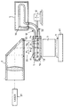
- a DUV excimer laser 21 with a wavelength of 157 nm forms an illumination system with optics 2, which is supplemented by a radial polarizer 22 according to DE 195 35 392 A. This produces a light beam 20 with radial polarization - indicated by the vectors P L and P R - and the optical axis A.
- This is formed here from M g F 2 with an orientation of the main axis in the direction of the optical axis A.
- the structures 11 are then created by the projection objective 3, for example a mirror objective, is imaged on the wafer 4, which is positioned on a support device 41.
- the structures 11 are arranged on the side of the carrier 10 facing the projection objective 3, since then the carrier material 10 is not arranged in the actual imaging beam path.
- the reticle 1 is attached to a positioning device 12.
- the reticle 1 is arranged between two plane-parallel cover plates (pellicles) 13, 14 made of material of suitable transparency, for example CaF 2 , BaF 2 or of the same orientation MgF 2 , which are connected to a line system 51, 52 and a cooling system 5.
- a fluid 50 preferably a gas, most suitably helium, can flow around the reticle 1. This enables effective temperature compensation between regions of the reticle 1 which are occupied differently by structure 11 or are irradiated differently by the light bundle 20, and overall cooling and temperature stabilization.
- Counter-current cooling of the front and back of reticle 1 is preferably used, as in the example.
- Fluoride crystal pellicles 13, 14 are also advantageous in connection with reticles made of other material, with or without Fluid cooling.
- Manufacturing is preferably 111-oriented Crystal plates made of classic and / or with ion beam be polished.
- the reticle according to the invention, the pellicle and the system are also suitable for a contact exposure system.
- the reticle according to the invention is useful. If circular polarization of light is introduced are all Effects of birefringence rotationally symmetrical to the optical Axis A and therefore tolerable in many ways.
Landscapes
- General Physics & Mathematics (AREA)
- Physics & Mathematics (AREA)
- Health & Medical Sciences (AREA)
- Epidemiology (AREA)
- Public Health (AREA)
- Environmental & Geological Engineering (AREA)
- Engineering & Computer Science (AREA)
- Life Sciences & Earth Sciences (AREA)
- Atmospheric Sciences (AREA)
- Toxicology (AREA)
- Exposure And Positioning Against Photoresist Photosensitive Materials (AREA)
- Crystals, And After-Treatments Of Crystals (AREA)
- Polarising Elements (AREA)
- Exposure Of Semiconductors, Excluding Electron Or Ion Beam Exposure (AREA)
- Preparing Plates And Mask In Photomechanical Process (AREA)
Abstract
Description
- Figur 1
- zeigt schematisch eine Projektionsbelichtungsanlage der erfindungsgemäßen Art.
Claims (12)
- Retikel mit Trägermaterial (10) aus transparentem optisch einachsigem Kristall, dadurch gekennzeichnet, daß die Hauptachse (A) des Kristalls nahezu senkrecht zur Fläche des Retikels (1) steht.
- Retikel aufbauend auf MgF2 als Trägermaterial (10), dadurch gekennzeichnet, daß die Hauptachse (A) des MgF2 nahezu senkrecht zur Retikel-Fläche (1) orientiert ist.
- Retikel nach Anspruch 1 oder Anspruch 2, dadurch gekennzeichnet, daß die Hauptachse mit ± 5° senkrecht zur Fläche des Retikels (1) orientiert ist.
- Retikel nach mindestens einem der Ansprüche 1-3, dadurch gekennzeichnet, daß es mit einer Kühlvorrichtung (5, 13, 14, 50, 51, 52) versehen ist.
- Retikel nach Anspruch 4, dadurch gekennzeichnet, daß die Kühlvorrichtung (5, 13, 14, 50, 51, 52) ein strömendes Fluid (50) aufweist.
- Belichtungsanlage der Mikrolithographie mit einem Beleuchtungssystem (2) und einem Retikel (1) mit Magnesiumfluorid als Trägermaterial (10), dadurch gekennzeichnet, daß das Beleuchtungssystem (2) radial polarisiertes Licht (20, PL, PR) bereitstellt und das Magnesiumfluorid mit seiner Kristall-Hauptachse nahezu in Richtung der optischen Achse (A) am Retikel (1) orientiert ist.
- Belichtungsanlage der Mikrolithographie mit einem Beleuchtungssystem (2), einem Retikel (1) mit Trägermaterial (10) aus transparentem optisch einachsigem Kristall, dadurch gekennzeichnet, daß das Beleuchtungssystem radial polarisiertes Licht (20, PL, PR) bereitstellt und das Trägermaterial (10) mit seiner Hauptachse nahezu in Richtung der optischen Achse (A) am Retikel (1) orientiert ist.
- Belichtungsanlage nach Anspruch 6 oder 7 mit einem Retikel nach mindestens einem der Ansprüche 3-5.
- Retikel (1) mit Trägermaterial (10) aus Kristall, gekennzeichnet durch eine Fluidkühlung.
- Retikel (1) nach Anspruch 9, dadurch gekennzeichnet, daß mindestens eine Planplatte (13, 14) parallel am Retikel (1) angeordnet ist und zwischen Retikel (1) und Planplatte (13, 14) ein Fluid (50) strömt.
- Retikel (1) nach Anspruch 10, dadurch gekennzeichnet, daß die Planplatte (13, 14) aus Kristall, insbesondere CaF2 oder MgF2 besteht.
- Pellicle (13, 14) aus Fluoridkristall, insbesondere CaF2, BaF2 oder MgF2.
Applications Claiming Priority (2)
| Application Number | Priority Date | Filing Date | Title |
|---|---|---|---|
| DE19808461A DE19808461A1 (de) | 1998-03-02 | 1998-03-02 | Retikel mit Kristall-Trägermaterial |
| DE19808461 | 1998-03-02 |
Publications (2)
| Publication Number | Publication Date |
|---|---|
| EP0940718A2 true EP0940718A2 (de) | 1999-09-08 |
| EP0940718A3 EP0940718A3 (de) | 2001-09-05 |
Family
ID=7859199
Family Applications (1)
| Application Number | Title | Priority Date | Filing Date |
|---|---|---|---|
| EP99102323A Withdrawn EP0940718A3 (de) | 1998-03-02 | 1999-02-06 | Retikel mit Kristall-Trägermaterial und Pellicle |
Country Status (6)
| Country | Link |
|---|---|
| US (1) | US6825913B1 (de) |
| EP (1) | EP0940718A3 (de) |
| JP (1) | JPH11316455A (de) |
| KR (1) | KR19990077475A (de) |
| DE (1) | DE19808461A1 (de) |
| TW (1) | TW538305B (de) |
Cited By (6)
| Publication number | Priority date | Publication date | Assignee | Title |
|---|---|---|---|---|
| WO2002059694A1 (en) * | 2001-01-26 | 2002-08-01 | Advanced Micro Devices, Inc. | A pellicle for use in small wavelength lithography and a method for making such a pellicule |
| EP1248148A1 (de) * | 2001-04-05 | 2002-10-09 | Asm Lithography B.V. | Lithographische Maske mit Schutzschicht |
| US6566626B2 (en) | 2001-07-03 | 2003-05-20 | Laserglass Ltd. | Method and apparatus for generating color images in a transparent medium |
| US6593035B1 (en) | 2001-01-26 | 2003-07-15 | Advanced Micro Devices, Inc. | Pellicle for use in small wavelength lithography and a method for making such a pellicle using polymer films |
| WO2011018418A1 (de) | 2009-08-11 | 2011-02-17 | Süss Microtec Lithography Gmbh | Verfahren und vorrichtung zum konstanthalten der maskenabmessungen |
| DE102009036953A1 (de) | 2009-08-11 | 2011-02-24 | Süss Micro Tec Lithography GmbH | Verfahren und Vorrichtung zum Konstanthalten der Maskenabmessungen in der Maskenebene bei der Lithografie |
Families Citing this family (3)
| Publication number | Priority date | Publication date | Assignee | Title |
|---|---|---|---|---|
| US20080186466A1 (en) * | 2005-04-12 | 2008-08-07 | Sirat Gabriel Y | Element for defocusing tm mode for lithography |
| KR101968675B1 (ko) * | 2010-06-25 | 2019-04-12 | 에이에스엠엘 네델란즈 비.브이. | 리소그래피 장치 및 방법 |
| WO2014067802A1 (en) * | 2012-10-31 | 2014-05-08 | Asml Holding N.V. | Patterning device support, lithographic apparatus, and method of controlling patterning device temperature |
Family Cites Families (22)
| Publication number | Priority date | Publication date | Assignee | Title |
|---|---|---|---|---|
| JPS5023595B1 (de) * | 1970-03-19 | 1975-08-08 | ||
| GB2139781B (en) * | 1983-05-13 | 1986-09-10 | American Telephone & Telegraph | Mask structure for vacuum ultraviolet lithography |
| US4604292A (en) | 1985-04-26 | 1986-08-05 | Spire Corporation | X-ray mask blank process |
| US4735877A (en) * | 1985-10-07 | 1988-04-05 | Canon Kabushiki Kaisha | Lithographic mask structure and lithographic process |
| JP2642637B2 (ja) * | 1987-08-18 | 1997-08-20 | 三井石油化学工業 株式会社 | 防塵膜 |
| JPH02166447A (ja) | 1988-12-20 | 1990-06-27 | Fujitsu Ltd | 露光用マスクおよびその製造方法 |
| US5088006A (en) | 1991-04-25 | 1992-02-11 | International Business Machines Corporation | Liquid film interface cooling system for semiconductor wafer processing |
| US5168001A (en) * | 1991-05-20 | 1992-12-01 | E. I. Du Pont De Nemours And Company | Perfluoropolymer coated pellicle |
| JP2945201B2 (ja) * | 1992-01-31 | 1999-09-06 | 信越化学工業株式会社 | ペリクル |
| JP2796005B2 (ja) * | 1992-02-10 | 1998-09-10 | 三菱電機株式会社 | 投影露光装置及び偏光子 |
| US5536604A (en) * | 1992-07-17 | 1996-07-16 | Kabushiki Kaisha Toshiba | Exposure mask |
| JP3244869B2 (ja) * | 1993-06-29 | 2002-01-07 | キヤノン株式会社 | 露光装置 |
| KR0166612B1 (ko) * | 1993-10-29 | 1999-02-01 | 가나이 쓰토무 | 패턴노광방법 및 그 장치와 그것에 이용되는 마스크와 그것을 이용하여 만들어진 반도체 집적회로 |
| JP3089153B2 (ja) * | 1993-12-13 | 2000-09-18 | 信越化学工業株式会社 | リソグラフィー用ペリクル |
| JP3445685B2 (ja) * | 1994-08-11 | 2003-09-08 | 三井化学株式会社 | マスク保護装置 |
| US5590148A (en) * | 1994-08-24 | 1996-12-31 | Duke University | Birefringent beamsplitter for high power lasers and laser applications |
| JP3290861B2 (ja) * | 1995-09-18 | 2002-06-10 | 株式会社東芝 | 露光用マスクとパターン形成方法 |
| US5935733A (en) * | 1996-04-05 | 1999-08-10 | Intel Corporation | Photolithography mask and method of fabrication |
| JPH1131647A (ja) * | 1997-07-11 | 1999-02-02 | Oki Electric Ind Co Ltd | 投影露光装置 |
| CA2283403C (en) * | 1998-01-22 | 2009-05-19 | Dai Nippon Printing Co., Ltd. | Diffraction grating-fabricating phase mask, and its fabrication method |
| US6197454B1 (en) * | 1998-12-29 | 2001-03-06 | Intel Corporation | Clean-enclosure window to protect photolithographic mask |
| US6150060A (en) * | 1999-01-11 | 2000-11-21 | The Regents Of The University Of California | Defect tolerant transmission lithography mask |
-
1998
- 1998-03-02 DE DE19808461A patent/DE19808461A1/de not_active Withdrawn
-
1999
- 1999-02-06 EP EP99102323A patent/EP0940718A3/de not_active Withdrawn
- 1999-02-25 TW TW088102804A patent/TW538305B/zh not_active IP Right Cessation
- 1999-02-25 KR KR1019990006261A patent/KR19990077475A/ko not_active Abandoned
- 1999-03-02 US US09/261,080 patent/US6825913B1/en not_active Expired - Fee Related
- 1999-03-02 JP JP5412399A patent/JPH11316455A/ja active Pending
Cited By (7)
| Publication number | Priority date | Publication date | Assignee | Title |
|---|---|---|---|---|
| WO2002059694A1 (en) * | 2001-01-26 | 2002-08-01 | Advanced Micro Devices, Inc. | A pellicle for use in small wavelength lithography and a method for making such a pellicule |
| US6544693B2 (en) | 2001-01-26 | 2003-04-08 | Advanced Micro Devices, Inc. | Pellicle for use in small wavelength lithography and a method for making such a pellicle |
| US6593035B1 (en) | 2001-01-26 | 2003-07-15 | Advanced Micro Devices, Inc. | Pellicle for use in small wavelength lithography and a method for making such a pellicle using polymer films |
| EP1248148A1 (de) * | 2001-04-05 | 2002-10-09 | Asm Lithography B.V. | Lithographische Maske mit Schutzschicht |
| US6566626B2 (en) | 2001-07-03 | 2003-05-20 | Laserglass Ltd. | Method and apparatus for generating color images in a transparent medium |
| WO2011018418A1 (de) | 2009-08-11 | 2011-02-17 | Süss Microtec Lithography Gmbh | Verfahren und vorrichtung zum konstanthalten der maskenabmessungen |
| DE102009036953A1 (de) | 2009-08-11 | 2011-02-24 | Süss Micro Tec Lithography GmbH | Verfahren und Vorrichtung zum Konstanthalten der Maskenabmessungen in der Maskenebene bei der Lithografie |
Also Published As
| Publication number | Publication date |
|---|---|
| EP0940718A3 (de) | 2001-09-05 |
| DE19808461A1 (de) | 1999-09-09 |
| TW538305B (en) | 2003-06-21 |
| US6825913B1 (en) | 2004-11-30 |
| JPH11316455A (ja) | 1999-11-16 |
| KR19990077475A (ko) | 1999-10-25 |
Similar Documents
| Publication | Publication Date | Title |
|---|---|---|
| EP0937999B1 (de) | Optisches System mit Polarisationskompensator | |
| EP1480082B1 (de) | Ringfeld-4-Spiegelsysteme mit konvexem Primärspiegel für die EUV-Lithographie | |
| EP1122608B1 (de) | Projektionsbelichtungsanlage mit reflektivem Retikel | |
| DE69531153T3 (de) | Optisches Projektionssystem mit Belichtungsgerät | |
| DE10127227A1 (de) | Katadioptrisches Reduktionsobjektiv | |
| DE102019217530A1 (de) | Optisches element und verfahren zum herstellen eines optischen elements | |
| EP1097404A1 (de) | Projektionsobjektiv für die mikrolithographie | |
| DE102007055567A1 (de) | Optisches System | |
| DE102010029905A1 (de) | Optisches System einer mikrolithographischen Projektionsbelichtungsanlage | |
| DE102012211256A1 (de) | Projektionsbelichtungsanlage für die Projektionslithographie | |
| DE102008040613A1 (de) | Optisches System einer mikrolithographischen Projektionsbelichtungsanlage | |
| EP1390783A2 (de) | Objektiv mit fluorid-kristall-linsen | |
| DE102007042047A1 (de) | Teilsystem einer Beleuchtungseinrichtung einer mikrolithographischen Projektionsbelichtungsanlage | |
| DE102016205619A1 (de) | Abschwächungsfilter für Projektionsobjektiv, Projektionsobjektiv mit Abschwächungsfilter für Projektionsbelichtungsanlage und Projektionsbelichtungsanlage mit Projektionsobjektiv | |
| DE10210782A1 (de) | Objektiv mit Kristall-Linsen | |
| DE102010041502A1 (de) | Spiegel, Projektionsobjektiv mit einem solchen Spiegel und Projektionsbelichtungs-anlage für die Mikrolithographie mit einem solchen Projektionsobjektiv | |
| WO2005040925A1 (de) | Euv-projektionsobjektiv mit spiegeln aus materialien mit unterschiedlichem vorzeichen der steigung der temperaturabhängigkeit des wärmeausdehnungskoeffizienten nahe der nulldurchgangstemperatur | |
| DE19808461A1 (de) | Retikel mit Kristall-Trägermaterial | |
| DE102021200790A1 (de) | Verfahren zum Betreiben eines optischen Systems, sowie Spiegel und optisches System | |
| DE102011003035A1 (de) | Polarisationsbeeinflussende optische Anordnung, sowie optisches System einer mikrolithographischen Projektionsbelichtungsanlage | |
| DE102006038454A1 (de) | Projektionsobjektiv einer mikrolithographischen Projektionsbelichtungsanlage | |
| DE102008054737A1 (de) | Mikrolithographische Projektionsbelichtungsanlage sowie Objektiv hierfür | |
| DE10127320A1 (de) | Objektiv mit Fluorid-Kristall-Linsen | |
| DE102012213553A1 (de) | Optisches System, insbesondere einer mikrolithographischen Projektionsbelichtungsanlage | |
| DE102022204833A1 (de) | Optisches system, lithographieanlage und verfahren zum herstellen eines optischen systems |
Legal Events
| Date | Code | Title | Description |
|---|---|---|---|
| PUAI | Public reference made under article 153(3) epc to a published international application that has entered the european phase |
Free format text: ORIGINAL CODE: 0009012 |
|
| AK | Designated contracting states |
Kind code of ref document: A2 Designated state(s): AT BE CH CY DE DK ES FI FR GB GR IE IT LI LU MC NL PT SE |
|
| AX | Request for extension of the european patent |
Free format text: AL;LT;LV;MK;RO;SI |
|
| PUAL | Search report despatched |
Free format text: ORIGINAL CODE: 0009013 |
|
| AK | Designated contracting states |
Kind code of ref document: A3 Designated state(s): AT BE CH CY DE DK ES FI FR GB GR IE IT LI LU MC NL PT SE |
|
| AX | Request for extension of the european patent |
Free format text: AL;LT;LV;MK;RO;SI |
|
| 17P | Request for examination filed |
Effective date: 20020129 |
|
| AKX | Designation fees paid |
Free format text: DE FR GB IE IT NL |
|
| RAP1 | Party data changed (applicant data changed or rights of an application transferred) |
Owner name: CARL ZEISS SMT AG |
|
| RAP1 | Party data changed (applicant data changed or rights of an application transferred) |
Owner name: CARL ZEISS SMT AG |
|
| RAP1 | Party data changed (applicant data changed or rights of an application transferred) |
Owner name: CARL ZEISS SMT AG |
|
| STAA | Information on the status of an ep patent application or granted ep patent |
Free format text: STATUS: THE APPLICATION IS DEEMED TO BE WITHDRAWN |
|
| 18D | Application deemed to be withdrawn |
Effective date: 20070901 |