EP0933802A1 - Process for the production of semiconductor device - Google Patents
Process for the production of semiconductor device Download PDFInfo
- Publication number
- EP0933802A1 EP0933802A1 EP97911513A EP97911513A EP0933802A1 EP 0933802 A1 EP0933802 A1 EP 0933802A1 EP 97911513 A EP97911513 A EP 97911513A EP 97911513 A EP97911513 A EP 97911513A EP 0933802 A1 EP0933802 A1 EP 0933802A1
- Authority
- EP
- European Patent Office
- Prior art keywords
- film
- plasma
- etching
- containing carbon
- fluorine containing
- Prior art date
- Legal status (The legal status is an assumption and is not a legal conclusion. Google has not performed a legal analysis and makes no representation as to the accuracy of the status listed.)
- Granted
Links
Images


Classifications
-
- H—ELECTRICITY
- H01—ELECTRIC ELEMENTS
- H01L—SEMICONDUCTOR DEVICES NOT COVERED BY CLASS H10
- H01L21/00—Processes or apparatus adapted for the manufacture or treatment of semiconductor or solid state devices or of parts thereof
- H01L21/02—Manufacture or treatment of semiconductor devices or of parts thereof
- H01L21/04—Manufacture or treatment of semiconductor devices or of parts thereof the devices having at least one potential-jump barrier or surface barrier, e.g. PN junction, depletion layer or carrier concentration layer
- H01L21/18—Manufacture or treatment of semiconductor devices or of parts thereof the devices having at least one potential-jump barrier or surface barrier, e.g. PN junction, depletion layer or carrier concentration layer the devices having semiconductor bodies comprising elements of Group IV of the Periodic System or AIIIBV compounds with or without impurities, e.g. doping materials
- H01L21/30—Treatment of semiconductor bodies using processes or apparatus not provided for in groups H01L21/20 - H01L21/26
- H01L21/302—Treatment of semiconductor bodies using processes or apparatus not provided for in groups H01L21/20 - H01L21/26 to change their surface-physical characteristics or shape, e.g. etching, polishing, cutting
- H01L21/306—Chemical or electrical treatment, e.g. electrolytic etching
- H01L21/3065—Plasma etching; Reactive-ion etching
-
- H—ELECTRICITY
- H01—ELECTRIC ELEMENTS
- H01L—SEMICONDUCTOR DEVICES NOT COVERED BY CLASS H10
- H01L21/00—Processes or apparatus adapted for the manufacture or treatment of semiconductor or solid state devices or of parts thereof
- H01L21/02—Manufacture or treatment of semiconductor devices or of parts thereof
- H01L21/04—Manufacture or treatment of semiconductor devices or of parts thereof the devices having at least one potential-jump barrier or surface barrier, e.g. PN junction, depletion layer or carrier concentration layer
- H01L21/18—Manufacture or treatment of semiconductor devices or of parts thereof the devices having at least one potential-jump barrier or surface barrier, e.g. PN junction, depletion layer or carrier concentration layer the devices having semiconductor bodies comprising elements of Group IV of the Periodic System or AIIIBV compounds with or without impurities, e.g. doping materials
- H01L21/30—Treatment of semiconductor bodies using processes or apparatus not provided for in groups H01L21/20 - H01L21/26
- H01L21/31—Treatment of semiconductor bodies using processes or apparatus not provided for in groups H01L21/20 - H01L21/26 to form insulating layers thereon, e.g. for masking or by using photolithographic techniques; After treatment of these layers; Selection of materials for these layers
- H01L21/3105—After-treatment
- H01L21/311—Etching the insulating layers by chemical or physical means
- H01L21/31144—Etching the insulating layers by chemical or physical means using masks
-
- H—ELECTRICITY
- H01—ELECTRIC ELEMENTS
- H01L—SEMICONDUCTOR DEVICES NOT COVERED BY CLASS H10
- H01L21/00—Processes or apparatus adapted for the manufacture or treatment of semiconductor or solid state devices or of parts thereof
- H01L21/02—Manufacture or treatment of semiconductor devices or of parts thereof
- H01L21/04—Manufacture or treatment of semiconductor devices or of parts thereof the devices having at least one potential-jump barrier or surface barrier, e.g. PN junction, depletion layer or carrier concentration layer
- H01L21/18—Manufacture or treatment of semiconductor devices or of parts thereof the devices having at least one potential-jump barrier or surface barrier, e.g. PN junction, depletion layer or carrier concentration layer the devices having semiconductor bodies comprising elements of Group IV of the Periodic System or AIIIBV compounds with or without impurities, e.g. doping materials
- H01L21/30—Treatment of semiconductor bodies using processes or apparatus not provided for in groups H01L21/20 - H01L21/26
- H01L21/31—Treatment of semiconductor bodies using processes or apparatus not provided for in groups H01L21/20 - H01L21/26 to form insulating layers thereon, e.g. for masking or by using photolithographic techniques; After treatment of these layers; Selection of materials for these layers
- H01L21/3105—After-treatment
- H01L21/311—Etching the insulating layers by chemical or physical means
- H01L21/31127—Etching organic layers
- H01L21/31133—Etching organic layers by chemical means
- H01L21/31138—Etching organic layers by chemical means by dry-etching
-
- H—ELECTRICITY
- H01—ELECTRIC ELEMENTS
- H01L—SEMICONDUCTOR DEVICES NOT COVERED BY CLASS H10
- H01L21/00—Processes or apparatus adapted for the manufacture or treatment of semiconductor or solid state devices or of parts thereof
- H01L21/70—Manufacture or treatment of devices consisting of a plurality of solid state components formed in or on a common substrate or of parts thereof; Manufacture of integrated circuit devices or of parts thereof
- H01L21/71—Manufacture of specific parts of devices defined in group H01L21/70
- H01L21/768—Applying interconnections to be used for carrying current between separate components within a device comprising conductors and dielectrics
- H01L21/76801—Applying interconnections to be used for carrying current between separate components within a device comprising conductors and dielectrics characterised by the formation and the after-treatment of the dielectrics, e.g. smoothing
- H01L21/76802—Applying interconnections to be used for carrying current between separate components within a device comprising conductors and dielectrics characterised by the formation and the after-treatment of the dielectrics, e.g. smoothing by forming openings in dielectrics
-
- H—ELECTRICITY
- H01—ELECTRIC ELEMENTS
- H01L—SEMICONDUCTOR DEVICES NOT COVERED BY CLASS H10
- H01L23/00—Details of semiconductor or other solid state devices
- H01L23/52—Arrangements for conducting electric current within the device in operation from one component to another, i.e. interconnections, e.g. wires, lead frames
- H01L23/522—Arrangements for conducting electric current within the device in operation from one component to another, i.e. interconnections, e.g. wires, lead frames including external interconnections consisting of a multilayer structure of conductive and insulating layers inseparably formed on the semiconductor body
- H01L23/5226—Via connections in a multilevel interconnection structure
-
- H—ELECTRICITY
- H01—ELECTRIC ELEMENTS
- H01L—SEMICONDUCTOR DEVICES NOT COVERED BY CLASS H10
- H01L23/00—Details of semiconductor or other solid state devices
- H01L23/52—Arrangements for conducting electric current within the device in operation from one component to another, i.e. interconnections, e.g. wires, lead frames
- H01L23/522—Arrangements for conducting electric current within the device in operation from one component to another, i.e. interconnections, e.g. wires, lead frames including external interconnections consisting of a multilayer structure of conductive and insulating layers inseparably formed on the semiconductor body
- H01L23/532—Arrangements for conducting electric current within the device in operation from one component to another, i.e. interconnections, e.g. wires, lead frames including external interconnections consisting of a multilayer structure of conductive and insulating layers inseparably formed on the semiconductor body characterised by the materials
- H01L23/5329—Insulating materials
-
- H—ELECTRICITY
- H01—ELECTRIC ELEMENTS
- H01L—SEMICONDUCTOR DEVICES NOT COVERED BY CLASS H10
- H01L2924/00—Indexing scheme for arrangements or methods for connecting or disconnecting semiconductor or solid-state bodies as covered by H01L24/00
- H01L2924/0001—Technical content checked by a classifier
- H01L2924/0002—Not covered by any one of groups H01L24/00, H01L24/00 and H01L2224/00
Definitions
- the present invention relates generally to a method for producing a semiconductor device using a fluorine containing carbon film.
- the relative dielectric constant of SiO 2 is about 4, and it has been diligently studied to dig up materials having a smaller relative dielectric constant than that of SiO 2 .
- SiOF having a relative dielectric constant of 3.5 into practice.
- the inventor has taken notice of a fluorine containing carbon film (for example, such as a fluorocarbon film) having a still smaller relative dielectric constant.
- the fluorine containing carbon film has many unknown factors, and a method for producing the fluorine containing carbon film itself has been searched.
- the fluorine containing carbon film can not be etched with a CF gas, such as CF 4 , which is used as an etching gas for a SiO 2 film, since the film itself to be etched is a CF material.
- the conventional processes can not be applied directly to the fluorine containing carbon film. Therefore, although the fluorine containing carbon film is suitable for an interlayer insulator film, there are many problems in order to put an interlayer insulator film of a fluorine containing carbon film into practice.
- the first invention of the present application is characterized by the steps of: depositing an insulator film of a fluorine containing carbon film on an object to be treated; forming a pattern of a resist film on the insulator film; and removing the resist film while etching the insulator film by an oxide plasma.
- this invention includes the following steps. When a predetermined recessed portion is formed on the insulator film by etching, the resist film may remain on the insulator film.
- the etch rate of the fluorine containing carbon film etched by the oxide plasma may be equal to the etch rate of the resist film etched by the oxide plasma.
- the second invention of the present invention is characterized by the steps of: depositing an insulator film of a fluorine containing carbon film on an object to be treated; forming a pattern of a resist film on the insulator film; and producing a plasma of a treatment gas containing an oxygen plasma producing gas and a silane compound gas, and removing the resist film while etching the fluorine containing carbon film by the produced plasma.
- the third invention of the present application is characterized by the steps of: depositing an insulator film of a fluorine containing carbon film on an object to be treated; depositing a protective coat resistant to an oxygen plasma, on the insulator film; forming a pattern of a resist film on the protective coat; etching the protective coat, which is exposed so as to correspond to the pattern of the resist film, to remove the protective coat; and removing the resist film while etching the fluorine containing carbon film by an oxygen plasma.
- the protective coat may be an insulator film or a conductive film.
- the fourth invention of the present application is characterized by the stops of: depositing an insulator film of a fluorine containing carbon film on an object to be treated; depositing a titanium nitride film on the insulator film; forming a pattern of a resist film on the insulator film; etching the titanium nitride film, which is exposed so as to correspond to the pattern of the resist film, to remove the titanium nitride film; and removing the resist film while etching the fluorine containing carbon film by an oxygen plasma.
- oxide on the metal layer is preferably removed by argon plasma after the fluorine containing carbon film is etched to expose the metal layer.
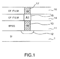
- FIGS. 1(a) and 1(b) an example of the structure of a semiconductor device produced by utilizing a method according to the present invention is shown in FIGS. 1(a) and 1(b).
- Reference number 1 denotes a silicon substrate
- 11 denotes a BPSG film (a film obtained by doping P and B into SiO 2 ).
- Reference number 12 is an n-type semiconductor region, and 13 denotes an electrode of, e.g., W (tungsten), which is embedded into a through hole of the BPSG film 11. These correspond to a part of a principal part of a circuit.
- an interconnection layer 15 of, e.g., aluminum is formed as a multilayer.
- the lower interconnection layer 15 is connected to an upper interconnection layer 15 (not shown) by means of a conductive layer 17 of, e.g., W, which is embedded into a via hole formed in an interlayer insulator film 16.
- FIG. 2(a) shows the state where, e.g., a number n interconnection layer of aluminum, is formed.
- a first interlayer insulator film 16 of a CF film is formed on an insulator film 14.
- the CF film can be deposited by the plasma CVD (Chemical Vapor Deposition) method using, e.g., a CF gas and a CH gas, as thin film deposition gases.
- a CF film having a thickness of, e.g., 0.7 ⁇ m, is deposited with gas and C 2 H 4 gas by means of an ECR (Electron Cyclotron Resonance) plasma treatment system, which also serves as an etching system and which will be described later.
- ECR Electro Cyclotron Resonance
- a resist film 18 of a predetermined pattern is formed on the surface of the CF film (the interlayer film 16).
- This resist film 18 is formed by applying a resist solution on the surface of the wafer using, e.g., the spin coating method, and then, carrying out exposure and development processes.
- the materials of the resist include organic materials, such as azide compounds, polyvinyl phenols, methacrylic acid compounds, novolak resins and polystyrene resins.
- the surface of the wafer is irradiated with O 2 plasma (oxygen plasma) to etch the CF film.
- O 2 plasma oxygen plasma
- an active species of O 2 cuts C-F bonds and C-C bonds to scatter as CO or CO 2 , and F also scatters as F 2 and so forth.
- the CF film is chemically etched with the O 2 plasma.
- the resist film 18 is an organic material
- the resist film 18 is also chemically etched with the O 2 plasma. Therefore, the etching of the CF film and the removing of the resist film 18 during the etching progress simultaneously.
- a predetermined via hole 19 is formed as shown in FIG.2(d). In order to accomplish this, the rate for removing the resist film 18 by the etching and the etch rate of the CF film may be previously recognized to set the thickness of the resist film 18.
- the rate for removing the resist film 18 by the etching is equal to the etch rate of the CF film, the surface of the CF film is planarized.
- a mechanical polishing process called CMP is generally carried out.
- CMP a mechanical polishing process
- the resist film 18 remains when the hole is formed, it is possible to remove the resist film and to form the hole without changing the thickness of the CF film by detecting the etching end time of the resist film 18 on the basis of, e.g., the quantity of emission of CO and CO 2 .
- the CF film is etched with O 2 gas and a silane gas, such as SiH 4 or gas, as shown in FIG. 3.
- a silane gas such as SiH 4 or gas
- FIG. 3 shows the state of such an etching.
- a protective coat 19a of SiO 2 is formed on the side wall of the hole 19 by the reaction of SiH 4 with O 2 , and the etching of the wide walls is inhibited.
- the side wall of the recessed portion 19 is also etched so that the recessed portion 19 expands laterally as shown in FIG, 4. This state is called bowing. Therefore, it is conceived that it is difficult to etch the recessed portion 19 of a high aspect ratio. According to the above technique, it is possible to etch a via hole or a through hole, which have a high aspect ratio. In this case, if the ratio of the silane gas to the O 2 gas is great, the protective coat grows excessively to deteriorate the shape of the recessed portion, so that it is required to set the mixing ratio of the silane gas in accordance with the etching conditions.
- This method may be combined with a method for forming an insulator film or a conductive film, which will be described later, on the surface of a CF film to be carried out.
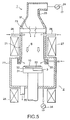
- the method of the present invention may be carried out by means of a plasma treatment system shown in FIG. 5.
- This system has a vacuum vessel 2 formed of aluminum or the like,
- the vacuum vessel 2 comprises: a cylindrical plasma chamber 21, which is arranged at an upper position, for producing plasma; and a cylindrical treatment chamber 22, which is arranged below the plasma chamber 21 to be communicated therewith and which has a larger diameter than that that of the plasma chamber 21. Furthermore, the vacuum vessel 2 is grounded to have zero potential.
- a transmission window 23 of a material capable of transmitting a micro wave e.g., quartz, is airtightly provided so as to maintain the vacuum state in the vacuum vessel 2.
- a waveguide 25 which is connected to a high-frequency power supply part 24 serving as a high-frequency supplying means for producing plasma of, e.g., 2.45 GHz.
- the micro wave M Produced by the high-frequency power supply part 24 is guided by the waveguide 25 to be introduced from the transmission window 23 into the plasma chamber 21.
- plasma gas nozzles 26 are arranged, e.g., at regular intervals in the circumferential directions thereof.
- a magnetic field forming means e.g., a ring-shaped main electromagnetic coil 27, is arranged so as to adjacent to the outer periphery of the side wall.
- a ring-shaped auxiliary electromagnetic coil 28 is arranged below the thin film deposition chamber 22 .
- a magnetic field extending downwards from the plasma chamber 21 to the treatment chamber 22, e.g., a magnetic field B of 875 gausses, can be formed so as to meet the ECR plasma conditions.
- permanent magnets may be substituted for the electromagnetic coils.
- the micro wave M having a controlled frequency and the magnetic field B are formed in the plasma chamber 21 to produce the ECR plasma by the interaction between the micro wave M and the magnetic field B.
- the resonance function occurs in the introduced gases at the aforementioned frequency to form a plasma at a high density. That is, this system forms an electron cyclotron resonance (ECR) plasma treatment system.
- ECR electron cyclotron resonance
- the mounting table 3 comprises a body 31 of, e.g. aluminum, and a ceramics body 33, which has a heater 32 therein and which is arranged on the body 31.
- the mounting surface functions as an electrostatic chuck.
- a high-frequency power supply part 34 for applying a bias voltage to draw ions into the wafer W is connected to the body 31 of the mounting table 3.
- An electrode for the bias voltage also serves as, e.g., an electrode for the electrostatic chuck.
- an exhaust pipe 35 is connected to the bottom of the vacuum vessel 2.
- reference number 30 denotes a ring-shaped thin film deposition gas supplying part for use in the thin film deposition treatment.
- a method for etching the wafer 10 serving as an object to be treated, using the above described system, will be described below.
- a gate valve (not shown) provided in the side wall of the vacuum vessel 2 is open, and the wafer 10 is introduced from a load-lock chamber (not shown) to be transferred onto the mounting table 3 by means of a transport arm (not shown).
- the internal atmosphere is exhausted through the exhaust pipe 35 to evacuate the interior of the vacuum vessel 2 to a predetermined degree of vacuum, and O 2 gas is introduced into the plasma chamber 21 from the plasma gas nozzle 26 as well as a silane gas, e.g., SiH 4 gas, is introduced into the plasma chamber 21 from the thin film deposition gas supplying part 30.
- a silane gas e.g., SiH 4 gas
- the pressure in the vacuum vessel 2 is maintained to be a predetermined process pressure, and a bias voltage of 13.56 MHz is applied to the mounting table 3 by means of the high-frequency power supply part 34.
- a high frequency wave (microwave) of 2.45 GHz produced from the plasma producing high-frequency power supply part 24 is carried in the waveguide 25 to reach the ceiling part of the vacuum vessel 2 to pass through the transmission window 23, so that the micro wave M is introduced into the plasma chamber 21.
- a magnetic field B of, e.g., 875 gausses , which is produced by the electromagnetic-coils 27 and 28, is applied from top to bottom.
- E electric field
- ⁇ B magnetic field
- the plasma flow which has flowed into the treatment chamber 22 from the plasma production chamber 21, is drawn into the wafer 10 by the bias voltage, so that the surface of the wafer 10 is etched.
- the inventor used the plasma treatment system, shown in FIG. 5 to prepare the wafer 10, on which a CF film was formed using C 4 F 8 gas and C 2 H 4 gas as thin film deposition gases and Ar gas as a plasma gas to form a pattern on the CF film by a resist film of an azide compound by means of a resist treatment system and an exposure system.
- O 2 gas was supplied to the wafer 10 from the plasma nozzle 26 at a flow rate of 100 sccm to form a hole having a width of 0.3 ⁇ m and an aspect ratio of 1 and simultaneously to etch the resist film.
- the process pressure was 0.2 Pa
- the micro wave power was 2500 W.
- the bias voltage was 1500 W
- the surface temperature of the mounting table 3 was 270 °C.
- Etching was carried out on the same conditions except that SiH 4 gas was supplied at 2 sccm, so that a good hole having an aspect ratio of 2 was formed.
- a conductive film, e.g., TiN (titanium nitride) film 41 which has a thickness of, e.g., 300 angstrom, is formed on the surface of a CF film 4 having a thickness D of, e.g., 8000 angstrom, as shown in FIG. 6(a).
- This TiN film 41 can be deposited with Ar gas and N 2 gas by the reactive sputtering using, e.g., Ti, as a target.
- a mask is formed on the surface of the TiN film 41 by the resist film 42 (FIG. 6(b)). Furthermore, the swell of the CF film is omitted in FIG. 6. Thereafter, the TiN film 41 is etched to the surface of the CF film 4 with a plasma of, e.g., BCl 3 , gas, as shown in FIG.6(c). This etching can be carried out by means of, e.g., the above described plasma treatment system. Then, the surface of the wafer is irradiated with O 2 plasma to etch the CF film 4 as well as to remove the resist film 42 by the etching (FIG. 6(d)).
- the TiN film 41 can function as a mask to etch only a region of the CF film corresponding to the pattern, so as to a predetermined via hole and a predetermined through hole (FIG. 7(a)).
- O 2 gas is switched to Ar gas to remove oxide from the surface of the interconnection layer of aluminum by the sputter etching using Ar ions (FIG. 7(b)).
- a metal 43 such as tungsten (W)
- W is embedded into the hole to form an interconnection layer as well as to form, e.g., a second interconnection layer (FIG. 7(c)).
- the embedding into the hole and the deposition of the interconnection layer may be carried out by the sputtering using aluminum.
- the CF film can be etched even if both of the resist film and the CF film do not resist to the O 2 plasma since the TiN film 41 functions as a so-called hard mask.
- the resist film 42 is removed during the etching of the CF film, it is required to carry out a process for removing the resist film 42 by the O 2 ashing serving as a post-treatment.
- the TiN film 41 functions as an adhesion layer for causing these metal layers to adhere to the CF film. Therefore, the resist film 42 does not have bad influence, so that it is not required to remove the resist film 42.
- undesired portions of the TiN film 41 can be removed simultaneously with the deposition of the interconnection layer, i.e., the etching of the metal layer.
- the adhesion layer is originally required, and TiN is conventionally used as the adhesion layer. Therefore, the method using TiN as a hard mask is an effective method since the method also forms the adhesion layer simultaneously.
- TiN is a conductive layer, it can be regarded as a part of the interconnection layer without being contained on the side of the interlayer insulator film, so that it is possible to prevent the relative dielectric constant of the interlayer insulator film from increasing.
- the waveguide is insured by the TiN film underlying the interconnection layer, so that it is possible to prevent the defective operation of the device.
- the conductive film may be made of any one of Al, W, Ti, TiW, TiWN and polysilicon, in addition to TiN.
- an insulator film may be used as the hard mask in place of the conductive film.
- the material of the insulator film may be, e.g., SiO 2 , SiOF or Si 3 N 4 .
- the insulator film is etched with, e.g., fluorine radicals using CF 4 gas.
- the next step e.g., the step of embedding aluminum and tungsten, may be carried out without removing the hard mask.
- all of the insulator film may be removed by, e.g., the wet etching using HF solution.
- the insulator film functions as a hard mask if the thickness thereof is not less than, eg., 100 angstrom.
- the thickness of the insulator film is preferably less than or equal to about one-third of the thickness of the CF film.
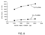
- FIG. 8 shows the results of the etching characteristics when etching the CF film with O 2 plasma and NF 3 plasma by means of the system shown in FIG. 5. It can be understood from this figure that O 2 plasma is effective for the etching of the CF film.
Abstract
Description
- The present invention relates generally to a method for producing a semiconductor device using a fluorine containing carbon film.
- In order to achieve high integration of a semiconductor device, it has been developed to provide devices, such as scale down of a pattern and multilayering of a circuit. As one of such devices, there is a technique for multilayering interconnection layers. In order to provide a multi layer metallization structure, a number n interconnection layer and a number (n+1) interconnection layer are connected to each other by means of a conductive layer, and a thin film called an interlayer insulator film is formed in a region other than the conductive layer.
- As one of typical interlayer insulator films, there is a SiO2 film. In recent years, in order to more accelerate operation of a device, it has been required to reduce the relative dielectric constant of the interlayer insulator film, and the material of the interlayer insulator film has been examined. That is, the relative dielectric constant of SiO2 is about 4, and it has been diligently studied to dig up materials having a smaller relative dielectric constant than that of SiO2. As one of such materials, it has been studied to put SiOF having a relative dielectric constant of 3.5 into practice. The inventor has taken notice of a fluorine containing carbon film (for example, such as a fluorocarbon film) having a still smaller relative dielectric constant.
- By the way, the fluorine containing carbon film has many unknown factors, and a method for producing the fluorine containing carbon film itself has been searched. For example, in conventional etching processes, the fluorine containing carbon film can not be etched with a CF gas, such as CF4, which is used as an etching gas for a SiO2 film, since the film itself to be etched is a CF material. Thus, the conventional processes can not be applied directly to the fluorine containing carbon film. Therefore, although the fluorine containing carbon film is suitable for an interlayer insulator film, there are many problems in order to put an interlayer insulator film of a fluorine containing carbon film into practice.
- It is therefore a principal object of the present invention to eliminate problems in an etching process and to enable to etch a fluorine containing carbon film to put an interlayer insulator film of a fluorine containing carbon film into practice.
- The first invention of the present application is characterized by the steps of: depositing an insulator film of a fluorine containing carbon film on an object to be treated; forming a pattern of a resist film on the insulator film; and removing the resist film while etching the insulator film by an oxide plasma. Specifically, this invention includes the following steps. When a predetermined recessed portion is formed on the insulator film by etching, the resist film may remain on the insulator film. The etch rate of the fluorine containing carbon film etched by the oxide plasma may be equal to the etch rate of the resist film etched by the oxide plasma.
- The second invention of the present invention is characterized by the steps of: depositing an insulator film of a fluorine containing carbon film on an object to be treated; forming a pattern of a resist film on the insulator film; and producing a plasma of a treatment gas containing an oxygen plasma producing gas and a silane compound gas, and removing the resist film while etching the fluorine containing carbon film by the produced plasma.
- The third invention of the present application is characterized by the steps of: depositing an insulator film of a fluorine containing carbon film on an object to be treated; depositing a protective coat resistant to an oxygen plasma, on the insulator film; forming a pattern of a resist film on the protective coat; etching the protective coat, which is exposed so as to correspond to the pattern of the resist film, to remove the protective coat; and removing the resist film while etching the fluorine containing carbon film by an oxygen plasma. In this case, the protective coat may be an insulator film or a conductive film.
- The fourth invention of the present application is characterized by the stops of: depositing an insulator film of a fluorine containing carbon film on an object to be treated; depositing a titanium nitride film on the insulator film; forming a pattern of a resist film on the insulator film; etching the titanium nitride film, which is exposed so as to correspond to the pattern of the resist film, to remove the titanium nitride film; and removing the resist film while etching the fluorine containing carbon film by an oxygen plasma.
- In the above cases, when a metal layer is formed below the fluorine containing carbon film, oxide on the metal layer is preferably removed by argon plasma after the fluorine containing carbon film is etched to expose the metal layer.
-
- FIG. 1 is a schematic diagram drawing showing a part of a semiconductor device produced by a method according to the present invention;
- FIG. 2 is a schematic diagram showing a preferred embodiment of a method according to the present invention;
- FIG. 3 is a schematic diagram showing another preferred embodiment of a method according to the present invention;
- FIG. 4 is a schematic diagram showing a method compared with a method according to the present invention;
- FIG. 5 is a longitudinal section of an example of a plasma treatment system for carrying out a method according to the present invention;
- FIG. 6 is a schematic diagram showing another preferred embodiment of the present invention;
- FIG. 7 is a schematic diagram showing another preferred embodiment of the present invention; and
- FIG. 8 is a characteristic diagram showing etching characteristics of a CF film.
-
- Although the preferred embodiments of the present invention are characterized by a process for etching a fluorine containing carbon film (for example, such as a fluorocarbon film) (which will be hereinafter referred to as a "CF film"), an example of the structure of a semiconductor device produced by utilizing a method according to the present invention is shown in FIGS. 1(a) and 1(b).
Reference number 1 denotes a silicon substrate, and 11 denotes a BPSG film (a film obtained by doping P and B into SiO2).Reference number 12 is an n-type semiconductor region, and 13 denotes an electrode of, e.g., W (tungsten), which is embedded into a through hole of the BPSG film 11.These correspond to a part of a principal part of a circuit. On the principal part of the circuit, aninterconnection layer 15 of, e.g., aluminum, is formed as a multilayer. Thelower interconnection layer 15 is connected to an upper interconnection layer 15 (not shown) by means of aconductive layer 17 of, e.g., W, which is embedded into a via hole formed in aninterlayer insulator film 16. - In order to produce such a semiconductor device, a process for etching the interlayer film will be described below. FIG. 2(a) shows the state where, e.g., a number n interconnection layer of aluminum, is formed. As shown in FIG. 2(b),a first
interlayer insulator film 16 of a CF film is formed on aninsulator film 14. The CF film can be deposited by the plasma CVD (Chemical Vapor Deposition) method using, e.g., a CF gas and a CH gas, as thin film deposition gases. For example, a CF film having a thickness of, e.g., 0.7 µm, is deposited withgas and C2H4 gas by means of an ECR (Electron Cyclotron Resonance) plasma treatment system, which also serves as an etching system and which will be described later.
- Then, as shown in FIG. 2(c), a
resist film 18 of a predetermined pattern is formed on the surface of the CF film (the interlayer film 16). This resistfilm 18 is formed by applying a resist solution on the surface of the wafer using, e.g., the spin coating method, and then, carrying out exposure and development processes. The materials of the resist include organic materials, such as azide compounds, polyvinyl phenols, methacrylic acid compounds, novolak resins and polystyrene resins. - Thereafter, the surface of the wafer is irradiated with O2 plasma (oxygen plasma) to etch the CF film. When the O2 plasma strikes the CF film, an active species of O2 cuts C-F bonds and C-C bonds to scatter as CO or CO2, and F also scatters as F2 and so forth. Thus, the CF film is chemically etched with the O2 plasma.
- By the way, since the
resist film 18 is an organic material, theresist film 18 is also chemically etched with the O2 plasma. Therefore, the etching of the CF film and the removing of theresist film 18 during the etching progress simultaneously. However, if the etching from the surface of the CF film to thealuminum interconnection layer 15 is completed before all theresist film 18 is removed by the etching, a predetermined viahole 19 is formed as shown in FIG.2(d). In order to accomplish this, the rate for removing theresist film 18 by the etching and the etch rate of the CF film may be previously recognized to set the thickness of theresist film 18. - If the rate for removing the
resist film 18 by the etching is equal to the etch rate of the CF film, the surface of the CF film is planarized. In order to planarize the surface of the interlayer insulator film after removing theresist film 18, a mechanical polishing process called CMP is generally carried out. However, in the above case, there is an advantage in that it is not required to carry out the CMP process. When the rate for removing the resist film by the etching is different from the etch rate or the CF film, it is desired to prevent all theresist film 18 from being removed before a predetermined hole is formed (before the surface of aluminum is etched). If theresist film 18 remains when the hole is formed, it is possible to remove the resist film and to form the hole without changing the thickness of the CF film by detecting the etching end time of theresist film 18 on the basis of, e.g., the quantity of emission of CO and CO2. - In another preferred embodiment of the present invention, the CF film is etched with O2 gas and a silane gas, such as SiH4 orgas, as shown in FIG. 3. FIG. 3 shows the state of such an etching. Simultaneously with the etching, a

protective coat 19a of SiO2 is formed on the side wall of thehole 19 by the reaction of SiH4 with O2, and the etching of the wide walls is inhibited. - When the etching is carried out by only O2 gas, the side wall of the
recessed portion 19 is also etched so that therecessed portion 19 expands laterally as shown in FIG, 4. This state is called bowing. Therefore, it is conceived that it is difficult to etch the recessedportion 19 of a high aspect ratio. According to the above technique, it is possible to etch a via hole or a through hole, which have a high aspect ratio. In this case, if the ratio of the silane gas to the O2 gas is great, the protective coat grows excessively to deteriorate the shape of the recessed portion, so that it is required to set the mixing ratio of the silane gas in accordance with the etching conditions. This method may be combined with a method for forming an insulator film or a conductive film, which will be described later, on the surface of a CF film to be carried out. - The method of the present invention may be carried out by means of a plasma treatment system shown in FIG. 5. This system has a
vacuum vessel 2 formed of aluminum or the like, Thevacuum vessel 2 comprises: acylindrical plasma chamber 21, which is arranged at an upper position, for producing plasma; and acylindrical treatment chamber 22, which is arranged below theplasma chamber 21 to be communicated therewith and which has a larger diameter than that that of theplasma chamber 21. Furthermore, thevacuum vessel 2 is grounded to have zero potential. - The upper end of the
vacuum vessel 2 is open. In this portion, atransmission window 23 of a material capable of transmitting a micro wave, e.g., quartz, is airtightly provided so as to maintain the vacuum state in thevacuum vessel 2. Outside of thetransmission window 23, there is provided awaveguide 25 which is connected to a high-frequencypower supply part 24 serving as a high-frequency supplying means for producing plasma of, e.g., 2.45 GHz. The micro wave M Produced by the high-frequencypower supply part 24 is guided by thewaveguide 25 to be introduced from thetransmission window 23 into theplasma chamber 21. On the side wall for dividing theplasma chamber 21,plasma gas nozzles 26 are arranged, e.g., at regular intervals in the circumferential directions thereof. - Around the outer periphery of the side wall far dividing the
plasma chamber 21, a magnetic field forming means, e.g., a ring-shaped mainelectromagnetic coil 27, is arranged so as to adjacent to the outer periphery of the side wall. Below the thinfilm deposition chamber 22, a ring-shaped auxiliaryelectromagnetic coil 28 is arranged. Thus, a magnetic field extending downwards from theplasma chamber 21 to thetreatment chamber 22, e.g., a magnetic field B of 875 gausses, can be formed so as to meet the ECR plasma conditions. Furthermore, permanent magnets may be substituted for the electromagnetic coils. - Thus, the micro wave M having a controlled frequency and the magnetic field B are formed in the
plasma chamber 21 to produce the ECR plasma by the interaction between the micro wave M and the magnetic field B. At this time, the resonance function occurs in the introduced gases at the aforementioned frequency to form a plasma at a high density. That is, this system forms an electron cyclotron resonance (ECR) plasma treatment system. - The mounting table 3 comprises a
body 31 of, e.g. aluminum, and aceramics body 33, which has aheater 32 therein and which is arranged on thebody 31. The mounting surface functions as an electrostatic chuck. To thebody 31 of the mounting table 3, e.g., a high-frequencypower supply part 34 for applying a bias voltage to draw ions into the wafer W is connected. An electrode for the bias voltage also serves as, e.g., an electrode for the electrostatic chuck. To the bottom of thevacuum vessel 2, anexhaust pipe 35 is connected. Furthermore,reference number 30 denotes a ring-shaped thin film deposition gas supplying part for use in the thin film deposition treatment. - A method for etching the
wafer 10 serving as an object to be treated, using the above described system, will be described below. First, a gate valve (not shown) provided in the side wall of thevacuum vessel 2 is open, and thewafer 10 is introduced from a load-lock chamber (not shown) to be transferred onto the mounting table 3 by means of a transport arm (not shown). - Subsequently, after the gate valve is closed to seal the interior of the
vacuum vessel 2, the internal atmosphere is exhausted through theexhaust pipe 35 to evacuate the interior of thevacuum vessel 2 to a predetermined degree of vacuum, and O2 gas is introduced into theplasma chamber 21 from theplasma gas nozzle 26 as well as a silane gas, e.g., SiH4 gas, is introduced into theplasma chamber 21 from the thin film depositiongas supplying part 30. Then, the pressure in thevacuum vessel 2 is maintained to be a predetermined process pressure, and a bias voltage of 13.56 MHz is applied to the mounting table 3 by means of the high-frequencypower supply part 34. - A high frequency wave (microwave) of 2.45 GHz produced from the plasma producing high-frequency
power supply part 24 is carried in thewaveguide 25 to reach the ceiling part of thevacuum vessel 2 to pass through thetransmission window 23, so that the micro wave M is introduced into theplasma chamber 21. In theplasma chamber 21, a magnetic field B of, e.g., 875 gausses , which is produced by the electromagnetic-coils - The plasma flow, which has flowed into the
treatment chamber 22 from theplasma production chamber 21, is drawn into thewafer 10 by the bias voltage, so that the surface of thewafer 10 is etched. - The inventor used the plasma treatment system, shown in FIG. 5 to prepare the
wafer 10, on which a CF film was formed using C4F8 gas and C2H4 gas as thin film deposition gases and Ar gas as a plasma gas to form a pattern on the CF film by a resist film of an azide compound by means of a resist treatment system and an exposure system. Using the plasma treatment system, O2 gas was supplied to thewafer 10 from theplasma nozzle 26 at a flow rate of 100 sccm to form a hole having a width of 0.3 µm and an aspect ratio of 1 and simultaneously to etch the resist film. In this case, the process pressure was 0.2 Pa, and the micro wave power was 2500 W. In addition, the bias voltage was 1500 W, and the surface temperature of the mounting table 3 was 270 °C. - Etching was carried out on the same conditions except that SiH4 gas was supplied at 2 sccm, so that a good hole having an aspect ratio of 2 was formed.
- Another preferred embodiment of the present invention will be described below. In this preferred embodiment, a conductive film, e.g., TiN (titanium nitride)
film 41, which has a thickness of, e.g., 300 angstrom, is formed on the surface of aCF film 4 having a thickness D of, e.g., 8000 angstrom, as shown in FIG. 6(a). ThisTiN film 41 can be deposited with Ar gas and N2 gas by the reactive sputtering using, e.g., Ti, as a target. - Subsequently, a mask is formed on the surface of the
TiN film 41 by the resist film 42 (FIG. 6(b)). Furthermore, the swell of the CF film is omitted in FIG. 6. Thereafter, theTiN film 41 is etched to the surface of theCF film 4 with a plasma of, e.g., BCl3, gas, as shown in FIG.6(c). This etching can be carried out by means of, e.g., the above described plasma treatment system. Then, the surface of the wafer is irradiated with O2 plasma to etch theCF film 4 as well as to remove the resistfilm 42 by the etching (FIG. 6(d)). - After the resist
film 42 is removed, theTiN film 41 can function as a mask to etch only a region of the CF film corresponding to the pattern, so as to a predetermined via hole and a predetermined through hole (FIG. 7(a)). When the etching of the CF film is completed to expose the surface of the interconnection layer of aluminum, O2 gas is switched to Ar gas to remove oxide from the surface of the interconnection layer of aluminum by the sputter etching using Ar ions (FIG. 7(b)). Thereafter, ametal 43, such as tungsten (W), is embedded into the hole to form an interconnection layer as well as to form, e.g., a second interconnection layer (FIG. 7(c)). The embedding into the hole and the deposition of the interconnection layer may be carried out by the sputtering using aluminum. - According to such a method, the CF film can be etched even if both of the resist film and the CF film do not resist to the O2 plasma since the
TiN film 41 functions as a so-called hard mask. In addition, since the resistfilm 42 is removed during the etching of the CF film, it is required to carry out a process for removing the resistfilm 42 by the O2 ashing serving as a post-treatment. When the tungsten layer and the aluminum layer are formed on the CF film, theTiN film 41 functions as an adhesion layer for causing these metal layers to adhere to the CF film. Therefore, the resistfilm 42 does not have bad influence, so that it is not required to remove the resistfilm 42. Furthermore, when undesired portions of theTiN film 41 can be removed simultaneously with the deposition of the interconnection layer, i.e., the etching of the metal layer. - When the metal layer is formed on the surface of the insulator film, the adhesion layer is originally required, and TiN is conventionally used as the adhesion layer. Therefore, the method using TiN as a hard mask is an effective method since the method also forms the adhesion layer simultaneously. In addition, since TiN is a conductive layer, it can be regarded as a part of the interconnection layer without being contained on the side of the interlayer insulator film, so that it is possible to prevent the relative dielectric constant of the interlayer insulator film from increasing. Moreover, even if the interconnection layer of aluminum is broken, the waveguide is insured by the TiN film underlying the interconnection layer, so that it is possible to prevent the defective operation of the device. The conductive film may be made of any one of Al, W, Ti, TiW, TiWN and polysilicon, in addition to TiN.
- According to the present invention, an insulator film may be used as the hard mask in place of the conductive film. The material of the insulator film may be, e.g., SiO2, SiOF or Si3N4. In this case, at a step of etching the insulator film (the above described step corresponding to FIG. 6(c)), the insulator film is etched with, e.g., fluorine radicals using CF4 gas.
- Since the hard mask is a part of the interlayer insulator film, the next step, e.g., the step of embedding aluminum and tungsten, may be carried out without removing the hard mask. Alternatively, all of the insulator film may be removed by, e.g., the wet etching using HF solution. When the insulator film is used as a hard mask, the insulator film functions as a hard mask if the thickness thereof is not less than, eg., 100 angstrom. However, if the thickness is too great when the insulator film remains in the device, the total relative dielectric constant of the interlayer insulator film including the insulator film is great, so that it is conceived that the thickness of the insulator film is preferably less than or equal to about one-third of the thickness of the CF film.
- FIG. 8 shows the results of the etching characteristics when etching the CF film with O2 plasma and NF3 plasma by means of the system shown in FIG. 5. It can be understood from this figure that O2 plasma is effective for the etching of the CF film.
- As described above, according to the present invention, it is possible to carry out the pattern etching of a CF film and to put an interlayer insulator film of, e.g., a CF film, into practice.
Claims (9)
- A method for producing a semiconductor device, which comprises the steps of:depositing an insulator film of a fluorine containing carbon film on an object to be treated;forming a pattern of a resist film on said insulator film; andremoving said resist film while etching said insulator film by an oxide plasma.
- A method for producing a semiconductor device, as set forth in claim 1, wherein said resist film remains on said insulator film when a predetermined recessed portion is formed on said insulator film by etching.
- A method for producing a semi conductor device, as set forth in claim 1, wherein an etch rate of said fluorine containing carbon film etched by the oxide plasma is equal to an etch rate of said resist film etched by the oxide plasma.
- A method for producing a semiconductor device, which comprises the steps of:depositing an insulator film of a fluorine containing carbon film on an object to be treated;forming a pattern of a resist film on said insulator film; andproducing a plasma of a treatment gas containing an oxygen plasma producing gas and a silane compound gas, and removing said resist film while etching said fluorine containing carbon film by the produced plasma.
- A method for producing a semiconductor device, which comprises the steps of:depositing an insulator film of a fluorine containing carbon film on an object to be treated;depositing a protective coat resistant to an oxygen plasma, on said insulator film;forming a pattern of a resist film on said protective coat;etching said protective coat, which is exposed so as to correspond to the pattern of the resist film, to remove the protective coat; andremoving said resist film while etching said fluorine containing carbon film by an oxygen plasma.
- A method for producing a semiconductor device, as set forth in claim 5, wherein said protective coat is an insulator film.
- A method for producing a semiconductor device, as set forth in claim 5, wherein said protective coat is a conductive film.
- A method for producing a semiconductor device, which comprises the steps of:depositing an insulator film of a fluorine containing carbon film on an object to be treated;depositing a titanium nitride film on said insulator film;forming a pattern of a resist film on said insulator film;etching said titanium nitride film, which is exposed so as to correspond to the pattern of the resist film, to remove the titanium nitride film; andremoving said resist film while etching said fluorine containing carbon film by an oxygen plasma.
- A method for producing a semiconductor device, as set forth in any one of claims 1 through 8, wherein a metal layer is formed below said fluorine containing carbon film, and after said fluorine containing carbon film is etched to expose said metal layer, oxide on the metal layer is removed by argon plasma.
Applications Claiming Priority (3)
| Application Number | Priority Date | Filing Date | Title |
|---|---|---|---|
| JP32091296A JP3400918B2 (en) | 1996-11-14 | 1996-11-14 | Method for manufacturing semiconductor device |
| JP32091296 | 1996-11-14 | ||
| PCT/JP1997/004099 WO1998021745A1 (en) | 1996-11-14 | 1997-11-11 | Process for the production of semiconductor device |
Publications (3)
| Publication Number | Publication Date |
|---|---|
| EP0933802A1 true EP0933802A1 (en) | 1999-08-04 |
| EP0933802A4 EP0933802A4 (en) | 1999-10-27 |
| EP0933802B1 EP0933802B1 (en) | 2002-04-17 |
Family
ID=18126663
Family Applications (1)
| Application Number | Title | Priority Date | Filing Date |
|---|---|---|---|
| EP97911513A Expired - Lifetime EP0933802B1 (en) | 1996-11-14 | 1997-11-11 | Process for the production of semiconductor device |
Country Status (7)
| Country | Link |
|---|---|
| US (1) | US6727182B2 (en) |
| EP (1) | EP0933802B1 (en) |
| JP (1) | JP3400918B2 (en) |
| KR (1) | KR100563610B1 (en) |
| DE (1) | DE69712080T2 (en) |
| TW (1) | TW349241B (en) |
| WO (1) | WO1998021745A1 (en) |
Cited By (4)
| Publication number | Priority date | Publication date | Assignee | Title |
|---|---|---|---|---|
| EP1035568A1 (en) * | 1997-11-20 | 2000-09-13 | Tokyo Electron Limited | Method of plasma processing |
| WO2001001471A1 (en) * | 1999-06-28 | 2001-01-04 | Lam Research Corporation | A method and apparatus for side wall passivation for organic etch |
| EP1146555A1 (en) * | 1999-03-09 | 2001-10-17 | Tokyo Electron Limited | Semiconductor device and production method therefor |
| US7838426B2 (en) | 2007-08-20 | 2010-11-23 | Lam Research Corporation | Mask trimming |
Families Citing this family (13)
| Publication number | Priority date | Publication date | Assignee | Title |
|---|---|---|---|---|
| KR100464384B1 (en) * | 1997-05-31 | 2005-02-28 | 삼성전자주식회사 | Method for forming VIA hole in semiconductor device |
| JP4260764B2 (en) * | 1999-03-09 | 2009-04-30 | 東京エレクトロン株式会社 | Manufacturing method of semiconductor device |
| KR100414611B1 (en) | 1999-03-09 | 2004-01-07 | 동경 엘렉트론 주식회사 | Production method for semiconductor device |
| JP3803523B2 (en) * | 1999-12-28 | 2006-08-02 | 株式会社東芝 | Dry etching method and semiconductor device manufacturing method |
| JP2001274143A (en) * | 2000-03-28 | 2001-10-05 | Tdk Corp | Dry etching method, micromachining method and mask for dry etching |
| JP3770790B2 (en) * | 2000-11-15 | 2006-04-26 | シャープ株式会社 | Ashing method |
| US6835663B2 (en) * | 2002-06-28 | 2004-12-28 | Infineon Technologies Ag | Hardmask of amorphous carbon-hydrogen (a-C:H) layers with tunable etch resistivity |
| US6865939B2 (en) * | 2002-09-16 | 2005-03-15 | Sandia Naitonal Laboratories | Fluorinated silica microchannel surfaces |
| JP4413556B2 (en) | 2003-08-15 | 2010-02-10 | 東京エレクトロン株式会社 | Film forming method, semiconductor device manufacturing method |
| JP2005123406A (en) * | 2003-10-16 | 2005-05-12 | Tokyo Electron Ltd | Plasma etching method |
| KR100780944B1 (en) * | 2005-10-12 | 2007-12-03 | 삼성전자주식회사 | Method for etching carbon-containing layer and method for manufacturing semiconductor device |
| JP4919871B2 (en) | 2007-02-09 | 2012-04-18 | 東京エレクトロン株式会社 | Etching method, semiconductor device manufacturing method, and storage medium |
| JP5261964B2 (en) * | 2007-04-10 | 2013-08-14 | 東京エレクトロン株式会社 | Manufacturing method of semiconductor device |
Citations (3)
| Publication number | Priority date | Publication date | Assignee | Title |
|---|---|---|---|---|
| US5442237A (en) * | 1991-10-21 | 1995-08-15 | Motorola Inc. | Semiconductor device having a low permittivity dielectric |
| WO1996012048A2 (en) * | 1994-10-11 | 1996-04-25 | Gelest, Inc. | Conformal titanium-based films and method for their preparation |
| WO1996019826A1 (en) * | 1994-12-20 | 1996-06-27 | National Semiconductor Corporation | A method of fabricating integrated circuits using bilayer dielectrics |
Family Cites Families (28)
| Publication number | Priority date | Publication date | Assignee | Title |
|---|---|---|---|---|
| JPS55107781A (en) | 1979-02-13 | 1980-08-19 | Fujitsu Ltd | Etching method for metal film |
| JPS6199332A (en) * | 1984-10-19 | 1986-05-17 | Fujitsu Ltd | Plasma etching method |
| JPH0697660B2 (en) | 1985-03-23 | 1994-11-30 | 日本電信電話株式会社 | Thin film formation method |
| JPS6243335A (en) | 1985-08-21 | 1987-02-25 | Arita Seisakusho:Kk | Open-door indicator for vehicle |
| JPS63233549A (en) | 1987-03-20 | 1988-09-29 | Nippon Telegr & Teleph Corp <Ntt> | Thin film formation |
| JPH033380A (en) | 1989-05-31 | 1991-01-09 | Mitsubishi Electric Corp | Gas laser device |
| JPH04271122A (en) | 1991-02-27 | 1992-09-28 | Fuji Electric Co Ltd | Plasma processing equipment |
| JPH0555575A (en) * | 1991-08-29 | 1993-03-05 | Sharp Corp | Semiconductor device |
| JPH05151619A (en) * | 1991-10-01 | 1993-06-18 | Ricoh Co Ltd | Optical information recording medium and recording method |
| US5417826A (en) | 1992-06-15 | 1995-05-23 | Micron Technology, Inc. | Removal of carbon-based polymer residues with ozone, useful in the cleaning of plasma reactors |
| US5489538A (en) * | 1992-08-21 | 1996-02-06 | Lsi Logic Corporation | Method of die burn-in |
| JPH06163479A (en) | 1992-11-17 | 1994-06-10 | Sony Corp | Dry etching method |
| JPH06196421A (en) | 1992-12-23 | 1994-07-15 | Sumitomo Metal Ind Ltd | Plasma device |
| JPH06264270A (en) * | 1993-03-09 | 1994-09-20 | Citizen Watch Co Ltd | Method for patterning hard carbon film |
| US5498657A (en) * | 1993-08-27 | 1996-03-12 | Asahi Glass Company Ltd. | Fluorine-containing polymer composition |
| JPH083842A (en) | 1994-06-15 | 1996-01-09 | Toyota Autom Loom Works Ltd | Monitoring device for loom |
| JP2748864B2 (en) | 1994-09-12 | 1998-05-13 | 日本電気株式会社 | Semiconductor device, method of manufacturing the same, method of manufacturing amorphous carbon film, and plasma CVD apparatus |
| JP2748879B2 (en) | 1995-02-23 | 1998-05-13 | 日本電気株式会社 | Method for producing fluorinated amorphous carbon film material |
| CA2157257C (en) * | 1994-09-12 | 1999-08-10 | Kazuhiko Endo | Semiconductor device with amorphous carbon layer and method of fabricating the same |
| US5654228A (en) * | 1995-03-17 | 1997-08-05 | Motorola | VCSEL having a self-aligned heat sink and method of making |
| US5905517A (en) * | 1995-04-12 | 1999-05-18 | Eastman Kodak Company | Heater structure and fabrication process for monolithic print heads |
| US5840455A (en) * | 1995-05-24 | 1998-11-24 | Ricoh Company, Ltd. | Electrophotographic photoconductor |
| JP3274324B2 (en) * | 1995-09-01 | 2002-04-15 | 株式会社東芝 | Method for manufacturing semiconductor device |
| US5733808A (en) * | 1996-01-16 | 1998-03-31 | Vanguard International Semiconductor Corporation | Method for fabricating a cylindrical capacitor for a semiconductor device |
| JP2956571B2 (en) * | 1996-03-07 | 1999-10-04 | 日本電気株式会社 | Semiconductor device |
| JP3228183B2 (en) * | 1996-12-02 | 2001-11-12 | 日本電気株式会社 | Insulating film, semiconductor device having the insulating film, and method of manufacturing the same |
| US5854134A (en) * | 1997-05-05 | 1998-12-29 | Taiwan Semiconductor Manufacturing Company Ltd. | Passivation layer for a metal film to prevent metal corrosion |
| US6066893A (en) * | 1997-09-24 | 2000-05-23 | Texas Instruments Incorporated | Contaminant resistant barriers to prevent outgassing |
-
1996
- 1996-11-14 JP JP32091296A patent/JP3400918B2/en not_active Expired - Fee Related
-
1997
- 1997-11-11 WO PCT/JP1997/004099 patent/WO1998021745A1/en active IP Right Grant
- 1997-11-11 DE DE69712080T patent/DE69712080T2/en not_active Expired - Lifetime
- 1997-11-11 US US09/101,308 patent/US6727182B2/en not_active Expired - Fee Related
- 1997-11-11 EP EP97911513A patent/EP0933802B1/en not_active Expired - Lifetime
- 1997-11-11 KR KR1019980705381A patent/KR100563610B1/en not_active IP Right Cessation
- 1997-11-13 TW TW086116927A patent/TW349241B/en not_active IP Right Cessation
Patent Citations (3)
| Publication number | Priority date | Publication date | Assignee | Title |
|---|---|---|---|---|
| US5442237A (en) * | 1991-10-21 | 1995-08-15 | Motorola Inc. | Semiconductor device having a low permittivity dielectric |
| WO1996012048A2 (en) * | 1994-10-11 | 1996-04-25 | Gelest, Inc. | Conformal titanium-based films and method for their preparation |
| WO1996019826A1 (en) * | 1994-12-20 | 1996-06-27 | National Semiconductor Corporation | A method of fabricating integrated circuits using bilayer dielectrics |
Non-Patent Citations (4)
| Title |
|---|
| H. V. JANSEN ET AL.: "Applications of fluorocarbons polymers in micromechanics and micromachining" SENSORS AND ACTUATORS A, vol. 41-42, 1 April 1994 (1994-04-01), pages 136-140, XP002112288 Switzerland * |
| PATENT ABSTRACTS OF JAPAN vol. 010, no. 279 (E-439), 20 September 1986 (1986-09-20) & JP 61 099332 A (FUJITSU LTD), 17 May 1986 (1986-05-17) * |
| PATENT ABSTRACTS OF JAPAN vol. 018, no. 678 (C-1290), 20 December 1994 (1994-12-20) & JP 06 264270 A (CITIZEN WATCH CO LTD), 20 September 1994 (1994-09-20) * |
| See also references of WO9821745A1 * |
Cited By (8)
| Publication number | Priority date | Publication date | Assignee | Title |
|---|---|---|---|---|
| EP1035568A1 (en) * | 1997-11-20 | 2000-09-13 | Tokyo Electron Limited | Method of plasma processing |
| EP1035568A4 (en) * | 1997-11-20 | 2001-01-31 | Tokyo Electron Ltd | Method of plasma processing |
| US6773762B1 (en) | 1997-11-20 | 2004-08-10 | Tokyo Electron Limited | Plasma treatment method |
| EP1146555A1 (en) * | 1999-03-09 | 2001-10-17 | Tokyo Electron Limited | Semiconductor device and production method therefor |
| EP1146555A4 (en) * | 1999-03-09 | 2004-12-29 | Tokyo Electron Ltd | Semiconductor device and production method therefor |
| WO2001001471A1 (en) * | 1999-06-28 | 2001-01-04 | Lam Research Corporation | A method and apparatus for side wall passivation for organic etch |
| US7838426B2 (en) | 2007-08-20 | 2010-11-23 | Lam Research Corporation | Mask trimming |
| US8864931B2 (en) | 2007-08-20 | 2014-10-21 | Lam Research Corporation | Mask trimming |
Also Published As
| Publication number | Publication date |
|---|---|
| EP0933802B1 (en) | 2002-04-17 |
| JP3400918B2 (en) | 2003-04-28 |
| TW349241B (en) | 1999-01-01 |
| US6727182B2 (en) | 2004-04-27 |
| DE69712080T2 (en) | 2002-11-14 |
| KR100563610B1 (en) | 2006-06-15 |
| EP0933802A4 (en) | 1999-10-27 |
| DE69712080D1 (en) | 2002-05-23 |
| KR19990077239A (en) | 1999-10-25 |
| JPH10144676A (en) | 1998-05-29 |
| WO1998021745A1 (en) | 1998-05-22 |
| US20010001741A1 (en) | 2001-05-24 |
Similar Documents
| Publication | Publication Date | Title |
|---|---|---|
| US6727182B2 (en) | Process for the production of semiconductor device | |
| KR100530246B1 (en) | Self-cleaning etch process | |
| JP4361625B2 (en) | Semiconductor device and manufacturing method thereof | |
| US6489248B2 (en) | Method and apparatus for etch passivating and etching a substrate | |
| EP1100119A1 (en) | Plasma processing method | |
| US6149730A (en) | Apparatus for forming films of a semiconductor device, a method of manufacturing a semiconductor device, and a method of forming thin films of a semiconductor | |
| US20070000870A1 (en) | Plasma processing method | |
| KR20020070255A (en) | Multiple stage cleaning for plasma etching chambers | |
| US6737350B1 (en) | Method of manufacturing semiconductor device | |
| KR100430807B1 (en) | Method of plasma-assisted film deposition | |
| US5916820A (en) | Thin film forming method and apparatus | |
| US6121154A (en) | Techniques for etching with a photoresist mask | |
| KR20190132948A (en) | Substrate processing method and substrate processing apparatus | |
| KR100838502B1 (en) | Method of producing semiconductor device | |
| JPH11154672A (en) | Plasma processing method | |
| JP2004363558A (en) | Manufacturing method of semiconductor device, and cleaning method of plasma etching device | |
| JP3961247B2 (en) | Plasma processing method, plasma processing apparatus, and semiconductor device manufacturing method | |
| US6492279B1 (en) | Plasma etching methods | |
| JP4381526B2 (en) | Plasma etching method | |
| JP4060450B2 (en) | Dry etching method | |
| US6329294B1 (en) | Method for removing photoresist mask used for etching of metal layer and other etching by-products | |
| WO2000017917A1 (en) | Plasma film forming method | |
| JPH11220024A (en) | Method and device for manufacturing semiconductor integrated circuit | |
| JPH11330063A (en) | Method for cleaning plasma processor | |
| JPH0927479A (en) | Dry etching method |
Legal Events
| Date | Code | Title | Description |
|---|---|---|---|
| PUAI | Public reference made under article 153(3) epc to a published international application that has entered the european phase |
Free format text: ORIGINAL CODE: 0009012 |
|
| 17P | Request for examination filed |
Effective date: 19981221 |
|
| AK | Designated contracting states |
Kind code of ref document: A1 Designated state(s): DE FR GB IT NL |
|
| RIC1 | Information provided on ipc code assigned before grant |
Free format text: 6H 01L 21/3065 A, 6H 01L 21/311 B |
|
| A4 | Supplementary search report drawn up and despatched |
Effective date: 19990913 |
|
| AK | Designated contracting states |
Kind code of ref document: A4 Designated state(s): DE FR GB IT NL |
|
| 17Q | First examination report despatched |
Effective date: 20000117 |
|
| GRAG | Despatch of communication of intention to grant |
Free format text: ORIGINAL CODE: EPIDOS AGRA |
|
| GRAG | Despatch of communication of intention to grant |
Free format text: ORIGINAL CODE: EPIDOS AGRA |
|
| GRAH | Despatch of communication of intention to grant a patent |
Free format text: ORIGINAL CODE: EPIDOS IGRA |
|
| REG | Reference to a national code |
Ref country code: GB Ref legal event code: IF02 |
|
| GRAH | Despatch of communication of intention to grant a patent |
Free format text: ORIGINAL CODE: EPIDOS IGRA |
|
| GRAA | (expected) grant |
Free format text: ORIGINAL CODE: 0009210 |
|
| STAA | Information on the status of an ep patent application or granted ep patent |
Free format text: STATUS: THE PATENT HAS BEEN GRANTED |
|
| AK | Designated contracting states |
Kind code of ref document: B1 Designated state(s): DE FR GB IT NL |
|
| RIN1 | Information on inventor provided before grant (corrected) |
Inventor name: HIRATA, TADASHI, 1004, DRAGON MANSION Inventor name: AOKI, TAKESHI Inventor name: ENDO, SHUNICHI Inventor name: ISHIZUKA, SHUICHI, 202, SHIROYAMA NEW HEIGHTS Inventor name: AKAHORI, TAKASHI |
|
| REF | Corresponds to: |
Ref document number: 69712080 Country of ref document: DE Date of ref document: 20020523 |
|
| ET | Fr: translation filed | ||
| PG25 | Lapsed in a contracting state [announced via postgrant information from national office to epo] |
Ref country code: GB Free format text: LAPSE BECAUSE OF NON-PAYMENT OF DUE FEES Effective date: 20021111 |
|
| PLBE | No opposition filed within time limit |
Free format text: ORIGINAL CODE: 0009261 |
|
| 26N | No opposition filed |
Effective date: 20030120 |
|
| GBPC | Gb: european patent ceased through non-payment of renewal fee | ||
| PGFP | Annual fee paid to national office [announced via postgrant information from national office to epo] |
Ref country code: NL Payment date: 20061115 Year of fee payment: 10 |
|
| PGFP | Annual fee paid to national office [announced via postgrant information from national office to epo] |
Ref country code: IT Payment date: 20061130 Year of fee payment: 10 |
|
| NLV4 | Nl: lapsed or anulled due to non-payment of the annual fee |
Effective date: 20080601 |
|
| PG25 | Lapsed in a contracting state [announced via postgrant information from national office to epo] |
Ref country code: NL Free format text: LAPSE BECAUSE OF NON-PAYMENT OF DUE FEES Effective date: 20080601 |
|
| PGFP | Annual fee paid to national office [announced via postgrant information from national office to epo] |
Ref country code: FR Payment date: 20081112 Year of fee payment: 12 |
|
| PG25 | Lapsed in a contracting state [announced via postgrant information from national office to epo] |
Ref country code: IT Free format text: LAPSE BECAUSE OF NON-PAYMENT OF DUE FEES Effective date: 20071111 |
|
| PGFP | Annual fee paid to national office [announced via postgrant information from national office to epo] |
Ref country code: DE Payment date: 20091105 Year of fee payment: 13 |
|
| REG | Reference to a national code |
Ref country code: FR Ref legal event code: ST Effective date: 20100730 |
|
| PG25 | Lapsed in a contracting state [announced via postgrant information from national office to epo] |
Ref country code: FR Free format text: LAPSE BECAUSE OF NON-PAYMENT OF DUE FEES Effective date: 20091130 |
|
| REG | Reference to a national code |
Ref country code: DE Ref legal event code: R119 Ref document number: 69712080 Country of ref document: DE Effective date: 20110601 Ref country code: DE Ref legal event code: R119 Ref document number: 69712080 Country of ref document: DE Effective date: 20110531 |
|
| PG25 | Lapsed in a contracting state [announced via postgrant information from national office to epo] |
Ref country code: DE Free format text: LAPSE BECAUSE OF NON-PAYMENT OF DUE FEES Effective date: 20110531 |