JP2005123406A - Plasma etching method - Google Patents
Plasma etching method Download PDFInfo
- Publication number
- JP2005123406A JP2005123406A JP2003356880A JP2003356880A JP2005123406A JP 2005123406 A JP2005123406 A JP 2005123406A JP 2003356880 A JP2003356880 A JP 2003356880A JP 2003356880 A JP2003356880 A JP 2003356880A JP 2005123406 A JP2005123406 A JP 2005123406A
- Authority
- JP
- Japan
- Prior art keywords
- etching
- gas
- film
- plasma
- fluorine
- Prior art date
- Legal status (The legal status is an assumption and is not a legal conclusion. Google has not performed a legal analysis and makes no representation as to the accuracy of the status listed.)
- Pending
Links
Images


Classifications
-
- H—ELECTRICITY
- H01—ELECTRIC ELEMENTS
- H01J—ELECTRIC DISCHARGE TUBES OR DISCHARGE LAMPS
- H01J37/00—Discharge tubes with provision for introducing objects or material to be exposed to the discharge, e.g. for the purpose of examination or processing thereof
- H01J37/32—Gas-filled discharge tubes
- H01J37/32009—Arrangements for generation of plasma specially adapted for examination or treatment of objects, e.g. plasma sources
- H01J37/32192—Microwave generated discharge
-
- H—ELECTRICITY
- H01—ELECTRIC ELEMENTS
- H01L—SEMICONDUCTOR DEVICES NOT COVERED BY CLASS H10
- H01L21/00—Processes or apparatus adapted for the manufacture or treatment of semiconductor or solid state devices or of parts thereof
- H01L21/02—Manufacture or treatment of semiconductor devices or of parts thereof
- H01L21/04—Manufacture or treatment of semiconductor devices or of parts thereof the devices having at least one potential-jump barrier or surface barrier, e.g. PN junction, depletion layer or carrier concentration layer
- H01L21/18—Manufacture or treatment of semiconductor devices or of parts thereof the devices having at least one potential-jump barrier or surface barrier, e.g. PN junction, depletion layer or carrier concentration layer the devices having semiconductor bodies comprising elements of Group IV of the Periodic System or AIIIBV compounds with or without impurities, e.g. doping materials
- H01L21/30—Treatment of semiconductor bodies using processes or apparatus not provided for in groups H01L21/20 - H01L21/26
- H01L21/31—Treatment of semiconductor bodies using processes or apparatus not provided for in groups H01L21/20 - H01L21/26 to form insulating layers thereon, e.g. for masking or by using photolithographic techniques; After treatment of these layers; Selection of materials for these layers
- H01L21/3105—After-treatment
- H01L21/311—Etching the insulating layers by chemical or physical means
- H01L21/31105—Etching inorganic layers
- H01L21/31111—Etching inorganic layers by chemical means
- H01L21/31116—Etching inorganic layers by chemical means by dry-etching
-
- H—ELECTRICITY
- H01—ELECTRIC ELEMENTS
- H01L—SEMICONDUCTOR DEVICES NOT COVERED BY CLASS H10
- H01L21/00—Processes or apparatus adapted for the manufacture or treatment of semiconductor or solid state devices or of parts thereof
- H01L21/02—Manufacture or treatment of semiconductor devices or of parts thereof
- H01L21/04—Manufacture or treatment of semiconductor devices or of parts thereof the devices having at least one potential-jump barrier or surface barrier, e.g. PN junction, depletion layer or carrier concentration layer
- H01L21/18—Manufacture or treatment of semiconductor devices or of parts thereof the devices having at least one potential-jump barrier or surface barrier, e.g. PN junction, depletion layer or carrier concentration layer the devices having semiconductor bodies comprising elements of Group IV of the Periodic System or AIIIBV compounds with or without impurities, e.g. doping materials
- H01L21/30—Treatment of semiconductor bodies using processes or apparatus not provided for in groups H01L21/20 - H01L21/26
- H01L21/31—Treatment of semiconductor bodies using processes or apparatus not provided for in groups H01L21/20 - H01L21/26 to form insulating layers thereon, e.g. for masking or by using photolithographic techniques; After treatment of these layers; Selection of materials for these layers
- H01L21/3105—After-treatment
- H01L21/311—Etching the insulating layers by chemical or physical means
- H01L21/31127—Etching organic layers
- H01L21/31133—Etching organic layers by chemical means
- H01L21/31138—Etching organic layers by chemical means by dry-etching
-
- H—ELECTRICITY
- H01—ELECTRIC ELEMENTS
- H01L—SEMICONDUCTOR DEVICES NOT COVERED BY CLASS H10
- H01L21/00—Processes or apparatus adapted for the manufacture or treatment of semiconductor or solid state devices or of parts thereof
- H01L21/02—Manufacture or treatment of semiconductor devices or of parts thereof
- H01L21/04—Manufacture or treatment of semiconductor devices or of parts thereof the devices having at least one potential-jump barrier or surface barrier, e.g. PN junction, depletion layer or carrier concentration layer
- H01L21/18—Manufacture or treatment of semiconductor devices or of parts thereof the devices having at least one potential-jump barrier or surface barrier, e.g. PN junction, depletion layer or carrier concentration layer the devices having semiconductor bodies comprising elements of Group IV of the Periodic System or AIIIBV compounds with or without impurities, e.g. doping materials
- H01L21/30—Treatment of semiconductor bodies using processes or apparatus not provided for in groups H01L21/20 - H01L21/26
- H01L21/31—Treatment of semiconductor bodies using processes or apparatus not provided for in groups H01L21/20 - H01L21/26 to form insulating layers thereon, e.g. for masking or by using photolithographic techniques; After treatment of these layers; Selection of materials for these layers
- H01L21/3105—After-treatment
- H01L21/311—Etching the insulating layers by chemical or physical means
- H01L21/31144—Etching the insulating layers by chemical or physical means using masks
Abstract
Description
本発明は、半導体装置を製造するための基板上に形成されたフッ素添加カーボン膜をプラズマによりエッチングする方法に関する。 The present invention relates to a method for etching a fluorine-added carbon film formed on a substrate for manufacturing a semiconductor device by plasma.
半導体装置の高集積化を図るための手法の一つとして配線を多層化する技術があり、多層配線構造をとるためには、n番目の配線層と(n+1)番目の配線層とを導電層で接続すると共に導電層以外の領域は層間絶縁膜と呼ばれる薄膜が形成される。この層間絶縁膜の代表的なものとしてSiO2膜があるが、近年デバイスの動作についてより一層の高速化を図るために層間絶縁膜の比誘電率を低くすることが要求されている。 As a technique for achieving high integration of semiconductor devices, there is a technique of multilayering wiring. In order to take a multilayer wiring structure, an nth wiring layer and an (n + 1) th wiring layer are connected to a conductive layer. In addition, a thin film called an interlayer insulating film is formed in the region other than the conductive layer. A typical example of the interlayer insulating film is a SiO2 film. In recent years, it has been required to lower the relative dielectric constant of the interlayer insulating film in order to further increase the operation speed of the device.
このような要請により、炭素(C)及びフッ素(F)の化合物であるフッ素添加カーボン膜(フロロカーボン膜)が注目されている。SiO2膜の比誘電率が4付近であるのに対して、フッ素添加カーボン膜は、原料ガスの種類を選定すれば比誘電率が例えば2.5以下になることから層間絶縁膜として極めて有効な膜である。そしてその成膜方法についても、原料ガスの選定が進み、また高密度で低電子温度のプラズマを発生させるCVD装置の開発により良質な膜が得られる見通しが立ってきており、低誘電率の絶縁膜としてフッ素添加カーボン膜の実用化が期待されている。 Due to such a demand, a fluorine-added carbon film (fluorocarbon film) which is a compound of carbon (C) and fluorine (F) has attracted attention. Whereas the relative dielectric constant of the SiO2 film is around 4, the fluorine-added carbon film is extremely effective as an interlayer insulating film because the relative dielectric constant is, for example, 2.5 or less if the type of source gas is selected. It is a membrane. As for the film formation method, the selection of source gases has progressed, and the development of CVD equipment that generates high-density, low-electron-temperature plasma is expected to provide a high-quality film. A practical application of a fluorine-added carbon film is expected as the film.
一方フッ素添加カーボン膜をエッチングする方法としては、酸素ガス及び窒素ガスをプラズマ化し、そのプラズマによりエッチングする方法が知られているが(特許文献1)、この場合酸素ラジカルと炭素とが反応して膜がいわば燃焼された格好になって側壁が除去され、そのためエッチング後の溝の断面形状が横に膨らんだ(アンダーカット)形状になってしまう課題がある。 On the other hand, as a method for etching a fluorine-added carbon film, a method is known in which oxygen gas and nitrogen gas are turned into plasma and etching is performed using the plasma (Patent Document 1). In this case, oxygen radicals react with carbon. There is a problem that the side wall is removed because the film is in a so-called burned state, and therefore the cross-sectional shape of the groove after etching becomes a shape that swells laterally (undercut).
またその他の方法としては、水素ガス及び窒素ガスをプラズマ化し、そのプラズマによりエッチングする方法が知られているが(非特許文献2)、この場合エッチングされたフッ素添加カーボン膜の側壁部に水素が入り込み、この水素が膜中のフッ素と結合してフッ化水素を生成してしまう。エッチングされた凹部内には、次工程でバリアメタル膜が形成されるかメタルが埋め込まれるが、フッ化水素が生成されると、バリアメタル膜あるいはメタルを腐食してダメージを与え、その結果これら膜との密着性が悪くなるという課題がある。 As another method, there is known a method in which hydrogen gas and nitrogen gas are turned into plasma and etching is performed using the plasma (Non-Patent Document 2). In this case, hydrogen is added to the side wall of the etched fluorine-added carbon film. The hydrogen enters and combines with fluorine in the film to generate hydrogen fluoride. In the etched recess, a barrier metal film is formed or metal is embedded in the next process. However, when hydrogen fluoride is generated, the barrier metal film or metal is corroded and damaged, and as a result, There is a problem that adhesion with the film is deteriorated.
本発明はこのような背景に基づいてなされたものであり、その目的は、フッ素添加カーボン膜に対して良好なエッチングを行うことができ、またエッチング後に他の膜にダメージを与えることのないプラズマエッチング方法を提供することにある。 The present invention has been made on the basis of such a background, and an object of the present invention is to make it possible to perform good etching on a fluorine-added carbon film and to prevent damage to other films after etching. It is to provide an etching method.
本発明は、半導体装置を製造するための基板上に形成されたフッ素添加カーボン膜をCxFy(x、yは自然数)ガスを含む処理ガスのプラズマによりエッチングすることを特徴とするプラズマエッチング方法である。CxFyガスとしては、例えばCF4ガス、C2F6ガス、C4F6ガス、C3F8ガス及びC4F8ガスなどを用いることができる。 The present invention is a plasma etching method characterized in that a fluorine-added carbon film formed on a substrate for manufacturing a semiconductor device is etched by plasma of a processing gas containing CxFy (x and y are natural numbers) gas. . As the CxFy gas, for example, CF4 gas, C2F6 gas, C4F6 gas, C3F8 gas, C4F8 gas and the like can be used.
本発明のプラズマエッチング方法の具体的な方法は、フッ素添加カーボン膜、ハードマスク及びパターンを形成するレジスト膜がこの順に積層され、半導体装置を製造するための基板をエッチングする方法において、
前記ハードマスクをエッチングして除去する工程と、
次いでCxFy(x、yは自然数)ガスを含む処理ガスのプラズマにより前記フッ素添加カーボン膜をエッチングして除去する工程と、
前記レジスト膜をエッチングして除去する工程と、を含むことを特徴とする。ハードマスクは、レジスト膜を例えば酸素の活性種によりエッチングするときにレジスト膜が除去された後、続いてフッ素添加カーボン膜もエッチングされてしまうことから、エッチングを止めるために用いられるものである。この方法において、ハードマスクをエッチングする工程は、例えばCxFy(x、yは自然数)ガスを含む処理ガスのプラズマが用いられるが、その他のガスのプラズマを用いてもよい。また前記ハードマスクをエッチングして除去する工程は、ハードマスクをエッチングしてハードマスクの一部を残す第1の段階と、残りのハードマスクをエッチングして除去する第2の段階と、に分け、前記レジスト膜をエッチングする工程は、第1の段階と第2の段階との間に行われるようにしてもよい。前記レジスト膜をエッチングする工程は、例えば酸素の活性種を含むプラズマにより行われる。
A specific method of the plasma etching method of the present invention is a method in which a fluorine-added carbon film, a hard mask, and a resist film for forming a pattern are laminated in this order, and a substrate for manufacturing a semiconductor device is etched.
Etching and removing the hard mask;
Next, etching and removing the fluorine-added carbon film with plasma of a processing gas containing CxFy (x and y are natural numbers) gas;
And a step of removing the resist film by etching. The hard mask is used to stop etching since the resist film is removed when the resist film is etched by, for example, active species of oxygen, and then the fluorine-added carbon film is also etched. In this method, the process of etching the hard mask uses, for example, plasma of a processing gas containing CxFy (x and y are natural numbers) gas, but plasma of other gases may be used. The process of removing the hard mask by etching is divided into a first stage in which the hard mask is etched to leave a part of the hard mask and a second stage in which the remaining hard mask is removed by etching. The step of etching the resist film may be performed between the first stage and the second stage. The step of etching the resist film is performed by, for example, plasma containing oxygen active species.
更に前記レジスト膜をエッチングする工程は、フッ素添加カーボン膜をエッチングして除去した後、酸素の活性種を含むプラズマを用いると共に、基板にバイアス電力を印加して下地膜であるハードマスクをプラズマ中の活性種によりスパッタしながら行われるようにしてもよく、この場合にはスパッタ物がフッ素添加カーボン膜の側壁の保護層の役割を果たし、このためレジスト膜のエッチング時(アッシング時)にフッ素添加カーボン膜の側壁がエッチングされることを抑制できる。またフッ素添加カーボン膜のエッチングは、処理ガスであるCxFy(x、yは自然数)ガスのプラズマのみにより行うようにしてもよいが、更に希ガスを添加した処理ガスのプラズマにより行うことが好ましい。 Further, in the step of etching the resist film, after removing the fluorine-added carbon film by etching, a plasma containing active species of oxygen is used, and a bias power is applied to the substrate so that the hard mask which is the base film is exposed to the plasma. In this case, the sputtered material serves as a protective layer for the side wall of the fluorine-added carbon film, so that fluorine is added during etching (ashing) of the resist film. It can suppress that the side wall of a carbon film is etched. Etching of the fluorine-added carbon film may be performed only with plasma of a processing gas CxFy (x and y are natural numbers), but is preferably performed with plasma of a processing gas to which a rare gas is added.
本発明によれば、フッ素添加カーボン膜を良好な形状でエッチングすることができ、また処理ガスとして水素を用いていないので、エッチングを行うことにより表面部に水素が入り込むことがなく、次工程で形成される膜に対してダメージを与えるおそれがない。 According to the present invention, the fluorine-added carbon film can be etched in a good shape, and since hydrogen is not used as a processing gas, hydrogen does not enter the surface portion by performing etching, and in the next step There is no risk of damaging the formed film.
本発明のプラズマエッチング方法の実施の形態を説明するにあたり、先ずこの方法に用いられる好ましいプラズマ処理装置について図1〜図3を参照しながら述べておく。図中1は、例えばアルミニウムからなる処理容器(真空チャンバ)であり、この処理容器1内には、載置台2が設けられている。この載置台2は表面部に静電チャック21が設けられており、この静電チャック21の電極は、スイッチ22を介して直流電源23に接続されている。また載置台2の内部には、温調手段である温調媒体の流路24が設けられており、流入路25からの温調媒体である冷媒が流路24内を通って流出路26から排出され、これにより載置台2上の基板である半導体ウエハ(以下ウエハという)Wが所定温度に維持されることとなる。また載置台2には例えば13.56MHzのバイアス用高周波電源27が接続されている。
In describing an embodiment of the plasma etching method of the present invention, a preferred plasma processing apparatus used in this method will be described with reference to FIGS. In the figure,
また載置台2の上方には、例えば平面形状が略円形状に構成された導電体からなるガス供給部3が設けられ、このガス供給部3における載置台2と対向する面には多数のガス供給孔31が形成されている。このガス供給部3の内部には、例えば図2に示すようにガス供給孔31と連通する格子状のガス流路32が形成されており、このガス流路32にはガス供給路33が接続されている。このガス供給路33には、図示しないガス供給源が接続されており、各ガス供給源からCxFy(x、yは自然数)ガスである例えばCF4ガス、希ガスである例えばAr(アルゴン)ガス、O2(酸素)ガス及びN2(窒素)ガスが当該ガス供給路33及びガス供給孔31を通じて処理容器1内に供給されることとなる。
Further, a
またガス供給部3には、図2に示すように当該ガス供給部3を貫通するように、多数の開口部34が形成されている。この開口部34は、プラズマを当該ガス供給部3の下方側の空間に通過させるためのものであり、例えば隣接するガス流路32同士の間に形成されている。また処理容器1の底部には排気管11が接続されており、この排気管11の基端側には図示しない真空排気手段が接続されている。更にまた処理容器1の内壁の内面側には、加熱手段であるヒータ12が設けられた囲い部材(ウオール部)13が設けられている。
In addition, a large number of
前記ガス供給部3の上部側には、誘電体例えば石英からなるプレート(マイクロ波透過窓)4が設けられ、この石英プレート4の上部側には、当該石英プレート4と密接するようにアンテナ部5が設けられている。この誘電体のプレートは石英に限らず例えばアルミナなどであってもよい。前記アンテナ部5は、図3にもに示すように、平面形状が円形の扁平なアンテナ本体50と、このアンテナ本体50の下面側に設けられ、多数のスロットが形成された円板状の平面アンテナ部材(スロット板)51とを備えている。これらアンテナ本体50と平面アンテナ部材51とは導体により構成されており、同軸導波管41に接続されている。アンテナ本体50は、この例では2つの部材に分割された構成となっており、図示しない外部からの冷媒流路を介して冷媒が通流する冷媒溜52が内部に形成されている。
A plate (microwave transmission window) 4 made of a dielectric material such as quartz is provided on the upper side of the
また前記平面アンテナ部材51とアンテナ本体50との間には、例えばアルミナや酸化ケイ素、窒化ケイ素等の低損失誘電体材料により構成された遅相板53が設けられている。この遅相板53はマイクロ波の波長を短くして前記導波管41内の管内波長を短くするためのものである。この実施の形態では、これらアンテナ本体50、平面アンテナ部材51及び遅相板53によりラジアルラインスロットアンテナ(RLSA)が構成されている。
Further, between the
このように構成されたアンテナ部5は、前記平面アンテナ部材51が石英プレート4に密接するように図示しないシール部材を介して処理容器1に装着されている。そしてこのアンテナ部5は同軸導波管41を介して外部のマイクロ波発生手段42と接続され、例えば周波数が2.45GHzあるいは8.4GHzのマイクロ波が供給されるようになっている。そして同軸導波管41の外側の導波管41Aはアンテナ本体50に接続され、中心導体41Bは遅相板53に形成された開口部を介して平面アンテナ部材51に接続されている。
The
前記平面アンテナ部材51は例えば厚さ0.3〜1mm程度の銅板からなり、図3に示すように例えば円偏波を発生させるための多数のスロット54が形成されている。このスロット54は略T字状に僅かに離間させて配置した一対のスロット54a,54bを1組として、当該平面アンテナ部材51の中央部を中心として周方向に沿って例えば同心円状や渦巻き状に形成されている。なおこのスロット54は略八字状に僅かに離間させて配置させてもよい。このようにスロット54aとスロット54bとを相互に略直交するような関係で配列しているので、2つの直交する偏波成分を含む円偏波が放射されることになる。この際スロット対54a,54bを遅相板53により圧縮されたマイクロ波の波長に対応した間隔で配列することにより、マイクロ波が平面アンテナ部材51から略平面波として放射される。
The
より具体的にはこの例では、各スロット54a,54bのスロット長が平面アンテナ部材51における同軸導波管41側のマイクロ波の波長の1/2以上の大きさであって、かつ平面アンテナ部材51におけるプラズマ発生空間(処理容器2内)側のマイクロ波の波長の1/2よりも小さい寸法に設定され、マイクロ波がスロット54を通ってプラズマ空間に入り、プラズマ空間からは同軸導波管41側に戻らないようになっている。なおスロットは、マイクロ波が円偏波ではなく直線偏波で放射されるように形成してもよい。
More specifically, in this example, the slot length of each of the slots 54a and 54b is equal to or greater than 1/2 the wavelength of the microwave on the
続いて半導体装置の製造プロセスの一部である、上記のプラズマ処理装置により実施されるエッチングプロセスの一例について説明する。半導体装置を製造するための基板であるウエハWは、図4(a)に示すように、エッチングの対象となっているフッ素添加カーボン膜(CF膜)61の上に例えばSiCNからなるハードマスク62が積層され、その上にパターンを形成するレジスト膜(レジストパターン)63が形成されている。またフッ素添加カーボン膜61の下にはハードマスク64を介してフッ素添加カーボン膜65が形成されている。即ちこの例では、フッ素添加カーボン膜65及び61が夫々n段目及びn+1段目の層間絶縁膜に相当する。フッ素添加カーボン膜65、61及びハードマスク62は、いずれもマイクロ波により発生させたプラズマを用いてCVDにより成膜されたものであり、フッ素添加カーボン膜65、61の膜厚は例えば5000Å、またハードマスク62の膜厚は例えば1000Åである。
Next, an example of an etching process performed by the plasma processing apparatus, which is a part of the semiconductor device manufacturing process, will be described. As shown in FIG. 4A, a wafer W, which is a substrate for manufacturing a semiconductor device, has a
先ず前記ウエハWを図示しないロードロック室から図1では見えない搬送口を介して処理容器1内に搬入し載置台2上に載置する。続いてガス供給部3からCF4ガス及びArガスを所定の流量で供給しながら、処理容器1の内部を真空排気して所定の圧力に維持すると共に、マイクロ波発生手段42から例えば2.45GHz、1500Wの高周波(マイクロ波)を供給すると共に高周波電源部27から例えば13.56MHz、1250Wののバイアス用高周波電力を載置台2に供給する。
First, the wafer W is loaded into the
前記マイクロ波は、TMモード或いはTEモード或いはTEMモードで同軸導波管41内を伝搬してアンテナ部5の平面アンテナ部材51に到達し、同軸導波管41の中心導体42Bを介して、平面アンテナ部材51の中心部から周縁領域に向けて放射状に伝搬される間に、スロット対54a,54bからマイクロ波が石英プレート4を介して下方側の空間に向けて放出される。
The microwave propagates in the
このとき既述のようにスロット対54a、54bを配列したので、円偏波が平面アンテナ部材51の平面に亘って均一に放出され、この下方の処理空間の電界密度が均一化される。一方ガス供給部3から処理容器1内に流出したCF4ガス及びArガスは、ガス供給部3の開口部34(図2参照)を通って上部側に拡散し、前記マイクロ波のエネルギ−によりプラズマが励起される。そしてこのプラズマは、前記開口部34を介してガス供給部3の下方側の処理空間に流れ込んで行き、露出しているハードマスク62が先ずプラズマ中の活性種によりエッチングされる。このハードマスク62のエッチングは、後述の実験例からも推測されるように、CF化合物が表面に付着してこの化合物と共に除去されていくものと考えられる。
At this time, since the slot pairs 54a and 54b are arranged as described above, circularly polarized waves are uniformly emitted over the plane of the
そして図4(b)に示すように、ハードマスク62が全部エッチングされる前において例えばハードマスク62の膜厚が元の膜厚の1/4程度になったときにガスの供給及び電力の供給を止めてプロセスを一旦停止し、レジスト膜63のエッチング(アッシング)プロセスに切り替える。このエッチングプロセスは、Arガス、O2ガス及びN2ガスをガス供給部3から処理容器1内に供給すると共に平面アンテナ部材51からマイクロ波を放出し、また載置台2に高周波バイアスを供給して行われる。混合ガスはマイクロ波のエネルギーによりプラズマ化され、そのプラズマ中の酸素活性種である酸素ラジカルによりレジスト膜63が灰化されて除去される(図4(c))。
Then, as shown in FIG. 4B, before all the
しかる後、ガスの供給及び電力の供給を止めてプロセスを一旦停止し、フッ素添加カーボン膜61のエッチングプロセスに切り替える。このエッチングプロセスは先のハードマスク62をエッチングしたときと同じ条件で行われる。エッチングのメカニズムは、後述の実験例から推測すると、プラズマ中にFの活性種やCFの活性種が発生し、これらの活性種がフッ素添加カーボン膜61と反応し、膜がCF2やCF3といった揮発性のガスとなって除去されていくものと考えられる。こうしてフッ素添加カーボン膜61がエッチングされ、図4(d)に示すように下地のハードマスク64が露出する。
Thereafter, the gas supply and power supply are stopped, the process is temporarily stopped, and the process is switched to the etching process of the fluorine-added
上述の実施の形態によれば、後述の実験例からも明らかなようにフッ素添加カーボン膜61のエッチング形状として良好な形状つまり垂直性の高いエッチング形状が得られる。そしてCxFyガスである例えばCF4ガスを用いており、水素ガスを使用していないので、エッチングにより形成されるフッ素添加カーボン膜の凹部の側壁面に、エッチングを行ったことに起因して水素が入り込むということがない。このため次工程で凹部に形成されるバリアメタル膜や凹部に埋め込まれるメタル膜にダメージを与えるおそれがなく、予定通りの電気的特性が得られる。
According to the above-described embodiment, as will be apparent from experimental examples described later, a favorable shape, that is, an etching shape with high perpendicularity, can be obtained as the etching shape of the fluorine-added
またハードマスクであるSiCN膜62のエッチング速度に対するフッ素添加カーボン膜61のエッチング速度の比である選択比を大きくとれることから、露出しているハードマスク62を全部エッチングせずに薄く残した後、レジスト膜63をエッチングし、その後残りのハードマスク62及びフッ素添加カーボン膜61をエッチングするという手法を採用できる。このためレジスト膜63のエッチング時に酸素ガスのプラズマがフッ素添加カーボン膜61に照射されないので、既述のアンダーカット(側壁が膨らんでエッチングされること)が起こらず、
従ってより一層垂直性の高い良好なエッチング形状が得られる。
In addition, since the selection ratio which is the ratio of the etching rate of the fluorine-added
Therefore, it is possible to obtain a good etching shape with higher verticality.
そしてまた上述のプラズマ処理装置によれば、円偏波が平面アンテナ部材51の平面に亘って均一に放出され、この下方の処理空間の電界密度が均一化されると共に、マイクロ波のエネルギーにより広い処理空間の全域に亘って高密度で欽一なプラズマが励起され、従って早いエッチング速度で均一な処理を行うことができる。
In addition, according to the plasma processing apparatus described above, circularly polarized waves are emitted uniformly over the plane of the
更に本発明の他の実施の形態について図5を参照しながら述べる。この実施の形態では、先の実施の形態で用いたと同様の表面構造(図5(a))を備えたウエハを用い、CF4ガス及びArガスをプラズマ化してエッチングする点では先の実施の形態と同様であるが、ハードマスク62のエッチングを途中で止めずに全部エッチングし(図5(b))、更に連続してフッ素添加カーボン膜61をエッチングして除去する(図5(c))。しかる後、酸素の活性種を含むプラズマを発生させながら、例えばArガス、N2ガス及びO2ガスのプラズマを発生させながら、載置台2に例えば500W〜1000W程度のバイアス電力を印加してレジスト膜63のエッチングを行う。
Further, another embodiment of the present invention will be described with reference to FIG. In this embodiment, a wafer having a surface structure similar to that used in the previous embodiment (FIG. 5A) is used, and CF4 gas and Ar gas are converted into plasma and etched. However, the etching of the
この実施の形態では、酸素の活性種によりレジスト膜63がエッチング(アッシング)されて除去される。またArイオンがフッ素添加カーボン膜61の下地膜であるハードマスク64をスパッタし、そのスパッタ物がフッ素添加カーボン膜61の凹部の側壁に付着していわば保護膜の役割を果たし、これにより酸素ラジカルが当該側壁をエッチングする作用が抑えられる、この結果凹部がアンダーカット形状にならずに良好な形状を維持できる。なおこの実施の形態において、Arガスの代わりに他の希ガスを添加してもよい。
In this embodiment, the resist
以上において、本発明にて用いられるCxFyガスとしては、CF4ガスに限らずC2F6ガス、C3F8ガス、C3F9ガス及びC4F8ガスなどを用いることができる。またハードマスクとしては、SiCN膜に限らず、SiO2膜、SiOF膜SiCO、SiCOHあるいはSi3N4膜などの絶縁膜であってもよく、これら絶縁膜はCF4ガスなどのCxFyガスによりエッチングすることができる。更にまたハードマスクは絶縁膜の代わりにTiNやTiWなどの導電膜であってもよく、この場合例えばハードマスクのエッチングを行うためのガスとしてBCl3ガスのプラズマを用いることができる。
In the above, the CxFy gas used in the present invention is not limited to CF4 gas, and C2F6 gas, C3F8 gas, C3F9 gas, C4F8 gas, and the like can be used. The hard mask is not limited to the SiCN film but may be an insulating film such as a
そしてレジスト膜63をエッチングして除去する工程は、ハードマスク62が残っている状態で行うことが好ましいが、ハードマスク62を除去し更にフッ素添加カーボン膜61をエッチングにより除去した後に行うようにしてもよい。なおフッ素添加カーボン膜61をエッチングするときに用いられる希ガスとしては、Arガスに限らずXeガスやKrガスなどであってもよい。
The step of removing the resist
本発明の効果を確認するために行った実験結果について以下に説明する。
(A.プラズマ処理装置における電子密度)
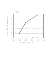
図1のプラズマ処理装置の処理容器1内にArガスを供給して圧力を夫々6.7Pa、67Pa及び133Paに設定し、マイクロ波パワーを2000Wに設定して石英プレート4の下方60mmの位置にてラングミュアプローブを用いて電子密度を計測した。結果は図6に示すとおりである。なお横軸のゼロは、載置台2上の中心位置に相当する。この結果から分かるように、電子密度がおよそ1×10¹² (個/cm3)であり、平行平板型プラズマ装置に比べておよそ10倍の大きさになっている。また電子温度は同位置において1.5eVであり、従って高密度、低電子温度のプラズマが得られることが分かる。
(B.エッチングによるフッ素添加カーボン膜の組成変化)
フッ素添加カーボン膜をエッチングするための処理ガスとして、CF4ガス及びArガスの混合ガス(Arガス/CF4ガス)を用いた場合と、既述の非特許文献2に記載されているH2ガス及びN2ガスの混合ガス(H2ガス/N2ガス)を用いた場合とについて、エッチングにより形成された凹部の側壁面の組成の違いを評価した。評価の方法は、図4に示した積層膜を備えたウエハを用いるのではなく、ウエハ表面全体にフッ素添加カーボン膜を成膜し、この基板を上記のプラズマ処理装置内に搬入し、バイアスは印加せずに2通りの処理ガスを用いてプラズマを発生させ、夫々フッ素添加カーボン膜のエッチングを行った。処理ガスとしては、流量を200/200sccmに設定したH2ガス/N2ガスと、流量を400/100sccmに設定したArガス/CF4ガスと、を用いた。このときのマイクロ波パワーは2000Wに設定し、圧力は1.33Pa(10mTorr)に設定し、プラズマの照射時間は30秒である。実際のエッチングにより形成される凹部の側壁には、加速されたイオンは衝突しないので、この側壁をモデル化するために載置台2に高周波バイアスを印加せずにエッチングを行った。
The results of experiments conducted to confirm the effects of the present invention will be described below.
(A. Electron density in plasma processing equipment)
Ar gas is supplied into the
(B. Composition change of fluorine-added carbon film by etching)
The case where a mixed gas of CF4 gas and Ar gas (Ar gas / CF4 gas) is used as a processing gas for etching the fluorine-added carbon film, and the H2 gas and N2 described in
そしてエッチングを行う前のフッ素添加カーボン膜の表面部、(H2ガス/N2ガス)によりエッチングを行ったときのフッ素添加カーボン膜の表面部、及び(Arガス/CF4ガス)によりエッチングを行ったときのフッ素添加カーボン膜の表面部について夫々XPS(X線光電子分光装置)によりCFの結合状態を調べたところ、図7(a)〜(c)に示す結果が得られた。 Then, the surface portion of the fluorine-added carbon film before etching, the surface portion of the fluorine-added carbon film when etched with (H2 gas / N2 gas), and the etching with (Ar gas / CF4 gas) When the bonding state of CF was examined by XPS (X-ray photoelectron spectrometer) on the surface portion of each of the fluorine-added carbon films, the results shown in FIGS. 7A to 7C were obtained.
H2ガス/N2ガスを用いた場合には、図7(a)に示す処理前のプロファイルに対し、図7(b)に示すようにCF2、CF3が減少する一方、C−CあるいはC−Hの結合が増加していることが分かる。そこでその表面部について、RBS(ラザフォードバックスキャッタリング)により膜中へのH(水素)の侵入深さを調べたところ、図8に示す結果が得られた。この結果からわかるように、H2ガス/N2ガスのプラズマを照射することで最表面から1000Å程度の深さにおいて、H原子の濃度がおよそ2.5倍増加している。なお図8には示されていないが、N(窒素)原子に関しては最表面で観察されるだけでフッ素添加カーボン膜中には侵入していなかった。これに対して水素は原子半径が小さいため膜中に容易に侵入し、拡散していると推察される。従ってフッ素添加カーボン膜に水素プラズマを照射するだけで水素が膜中深く侵入し、膜組成を変化させてしまうことが分かった。 When H2 gas / N2 gas is used, CF2 and CF3 decrease as shown in FIG. 7B, whereas CC or C-H, as compared to the profile before processing shown in FIG. 7A. It can be seen that the coupling of increases. Therefore, when the penetration depth of H (hydrogen) into the film was examined on the surface portion by RBS (Rutherford backscattering), the result shown in FIG. 8 was obtained. As can be seen from this result, the concentration of H atoms is increased by about 2.5 times at a depth of about 1000 mm from the outermost surface by irradiation with H2 gas / N2 gas plasma. Although not shown in FIG. 8, N (nitrogen) atoms were only observed on the outermost surface and did not penetrate into the fluorine-added carbon film. On the other hand, since hydrogen has a small atomic radius, it is assumed that hydrogen easily enters and diffuses into the film. Therefore, it was found that hydrogen can penetrate deeply into the film by simply irradiating the fluorine-added carbon film with hydrogen plasma and change the film composition.
一方Arガス/CF4ガスのプラズマを照射した場合には、図7(c)に示すように膜表面部のCF結合状態のプロファイルはほとんど変化しておらず、エッチングに形成される膜に対して水素によるダメージのおそれのないことが確認された。
(C.Arガス/CF4ガスの流量比とエッチング特性との関係)
CF4ガスによるフッ素添加カーボン膜のエッチングのメカニズムを調べるために、先ずArガス/CF4ガスの流量比とエッチング速度との関係を調べたところ、図9に示す結果が得られた。その他のプロセス条件については、マイクロ波パワー及びバイアスパワーが夫々1500W及び1250Wであり、圧力が1.33Paであり、ウエハ温度が40℃である。
On the other hand, when Ar gas / CF 4 plasma is irradiated, the profile of the CF bonding state on the surface of the film hardly changes as shown in FIG. It was confirmed that there was no risk of hydrogen damage.
(C. Relationship between flow ratio of Ar gas / CF4 gas and etching characteristics)
In order to investigate the etching mechanism of the fluorine-added carbon film with CF4 gas, first, the relationship between the flow rate ratio of Ar gas / CF4 gas and the etching rate was examined, and the result shown in FIG. 9 was obtained. For other process conditions, the microwave power and bias power are 1500 W and 1250 W, respectively, the pressure is 1.33 Pa, and the wafer temperature is 40 ° C.
図9から分かるように、CF4ガスの流量が少ないとエッチング速度が遅く、CF4ガスの添加量を増やしていくと、エッチング速度は急激に増加している。Arガスだけではスパッタ作用しかなく、ケミカルな反応によるエッチングは全く起こらず、また一般にC(炭素)は吸着係数が高く、F(フッ素)は揮発性が高いことが知られており、今回用いたフッ素添加カーボン膜はC/F比が1程度とCの比率が高いことから、スパッタだけではガス化が起こらないと考えられる。そしてCF4を添加していくことで、プラズマ中にFやCFといったエッチング種が発生してフッ素添加カーボン膜をエッチングし、膜表面部がCF2やCF3といった揮発性のガスとなって脱離し、エッチングが促進されたと推測される。
(D.高周波電力とエッチング特性との関係)
マイクロ波パワーとバイアスパワーとを変えながらフッ素添加カーボン膜のエッチング速度について等速度となるポイントをプロットして等速度線を求めたところ、図10に示す結果が得られた。その他のプロセス条件は、上記の項目C.D.に記載した条件と同じである。この結果から分かるように、エッチング速度は、マイクロ波パワー及びバイアスパワーのいずれを大きくしても増加し、特にマイクロ波パワーを大きくすることで、急激に増加している。これは、高密度プラズマによってCF4の解離が促進され、エッチング種の量が増加したことによると考えられる。
As can be seen from FIG. 9, the etching rate is slow when the flow rate of CF4 gas is small, and the etching rate increases rapidly as the amount of CF4 gas added is increased. Ar gas alone has only a sputtering effect, etching by chemical reaction does not occur at all, and C (carbon) is generally known to have a high adsorption coefficient and F (fluorine) is highly volatile. Since the fluorine-added carbon film has a C / F ratio of about 1 and a high C ratio, it is considered that gasification does not occur only by sputtering. By adding CF4, etching species such as F and CF are generated in the plasma and the fluorine-added carbon film is etched, and the film surface part is desorbed as a volatile gas such as CF2 and CF3. Is presumed to have been promoted.
(D. Relationship between high frequency power and etching characteristics)
When the constant velocity line was obtained by plotting the point at which the etching rate of the fluorine-added carbon film was equal while changing the microwave power and the bias power, the result shown in FIG. 10 was obtained. Other process conditions are described in item C.1 above. D. The conditions are the same as described in. As can be seen from this result, the etching rate increases when either the microwave power or the bias power is increased, and in particular, increases rapidly when the microwave power is increased. This is considered to be due to the fact that the dissociation of CF4 is promoted by the high-density plasma and the amount of etching species is increased.
また同様にしてハードマスクであるSiCN膜についてもエッチング速度の等速度線を求めたところ、図11に示す結果が得られた。SiCN膜のエッチング速度は、フッ素添加カーボン膜と異なり、プラズマ密度にはあまり依存せずにバイアスパワーに大きく依存していることが分かる。この結果からSiCN膜のエッチングはイオンの密度よりもイオンスパッタのエネルギーに支配されているといえる。また図12は、図10及び図11の関係から導き出した選択比(フッ素添加カーボン膜のエッチング速度/SiCN膜のエッチング速度)について等選択比となるポイント群を結んだマップであり、この結果からフッ素添加カーボン膜のエッチングを高速で行いかつ高選択比を得るための条件は、マイクロ波パワー、即ち高密度プラズマが必要で、バイアスパワーにはほとんど依存しないことが分かった。従って図6の結果から記述の図1に示したプラズマ処理装置は、フッ素添加カーボン膜のエッチングを行うための装置として有効であることが理解される。 Similarly, when an isokinetic line of the etching rate was obtained for the SiCN film as a hard mask, the result shown in FIG. 11 was obtained. It can be seen that the etching speed of the SiCN film differs greatly from the plasma density and greatly depends on the bias power, unlike the fluorine-added carbon film. From this result, it can be said that the etching of the SiCN film is dominated by the ion sputtering energy rather than the ion density. FIG. 12 is a map connecting point groups that are equal in selectivity ratio (etching rate of fluorine-added carbon film / etching rate of SiCN film) derived from the relationship of FIGS. 10 and 11. It has been found that the conditions for etching the fluorine-added carbon film at high speed and obtaining a high selectivity require microwave power, that is, high-density plasma, and hardly depend on the bias power. Therefore, it can be understood from the result of FIG. 6 that the plasma processing apparatus shown in FIG. 1 is effective as an apparatus for etching the fluorine-added carbon film.
(E.ウエハ温度とエッチング特性との関係)
マイクロ波パワー及びバイアスパワーを夫々1500W及び1250Wに設定し、圧力を1.33Paに設定し、Arガス/CF4ガスの流量を400/100sccmに設定し、ウエハの温度を0℃と40℃との2通りに設定して前記選択比及びエッチングされた凹部の側壁の角度に対する影響について調べたところ、図13及び図14に示す結果が得られた。
(E. Relationship between wafer temperature and etching characteristics)
The microwave power and bias power are set to 1500 W and 1250 W, respectively, the pressure is set to 1.33 Pa, the flow rate of Ar gas / CF 4 gas is set to 400/100 sccm, and the wafer temperature is set to 0 ° C. and 40 ° C. When the effect on the selection ratio and the angle of the side wall of the etched recess was examined with two settings, the results shown in FIGS. 13 and 14 were obtained.
図13から分かるように、ウエハの温度を高くすると選択比が向上する。これはSiCN膜のエッチング速度がウエハの温度上昇に伴って減少したためである。即ち、ウエハ温度の上昇に伴いエッチング時におけるSiCN膜表面のデポジション(堆積物)の量が減少し、それによってエッチング反応が抑制されたためと考えられる。ここでもし堆積物が保護膜として働くならばウエハ温度の上昇により堆積物が薄くなってSiCN膜のエッチング速度が大きくなり、選択比は小さくなるはずである。従ってSiCN膜のエッチングのメカニズムは、SiCN膜の表面に付着した堆積物が保護膜として働くのではなく、SiO2のエッチングのメカニズムのように、SiCN膜の表面にCF化合物が堆積し、その堆積物と一緒にSiCN膜が剥がれていくものと推測される。 As can be seen from FIG. 13, the selectivity increases as the wafer temperature increases. This is because the etching rate of the SiCN film decreases as the wafer temperature rises. That is, it is considered that the amount of deposition (deposits) on the surface of the SiCN film at the time of etching decreased with the increase in wafer temperature, thereby suppressing the etching reaction. Here, if the deposit acts as a protective film, the deposit becomes thinner and the etching rate of the SiCN film increases as the wafer temperature rises, and the selectivity should decrease. Therefore, the etching mechanism of the SiCN film is not the deposit attached to the surface of the SiCN film acting as a protective film, but the CF compound is deposited on the surface of the SiCN film like the etching mechanism of SiO2, and the deposit It is presumed that the SiCN film is peeled off together with the substrate.
また図14から分かるようにウエハ温度が高くなると凹部の側壁のウエハ表面に対する角度が垂直に近付いてくる。これは温度が上昇することでエッチング生成物がエッチングされた部分の側壁に吸着せずに排気されるという一般的な反応であると思われる。
(F.エッチング形状の観察及び他の処理ガスによるエッチング)
マイクロ波パワー及びバイアスパワーを夫々1500W及び1250Wに設定し、圧力を1.33Paに設定し、Arガス/CF4ガスの流量を400/100sccmに設定し、ウエハの温度を40℃に設定して、先ずフッ素添加カーボン膜の上に形成されているハードマスクであるSiCN膜をエッチングして除去し、次いでフッ素添加カーボン膜をエッチングした。フッ素添加カーボン膜及びハードマスクの膜厚は夫々5000Å及び1000Åである。このプロセスを実施例F−1とする。
As can be seen from FIG. 14, when the wafer temperature increases, the angle of the side wall of the recess with respect to the wafer surface approaches perpendicularly. This seems to be a general reaction in which the etching product is exhausted without being adsorbed on the side wall of the etched portion as the temperature rises.
(F. Observation of etching shape and etching with other processing gas)
The microwave power and bias power were set to 1500 W and 1250 W, respectively, the pressure was set to 1.33 Pa, the Ar gas / CF 4 gas flow rate was set to 400/100 sccm, and the wafer temperature was set to 40 ° C. First, the SiCN film, which is a hard mask formed on the fluorine-added carbon film, was removed by etching, and then the fluorine-added carbon film was etched. The film thicknesses of the fluorine-added carbon film and the hard mask are 5000 mm and 1000 mm, respectively. This process is referred to as Example F-1.
CF4ガスの代わりにC4F8ガスを用い、更にArガス及びO2ガスを用い、Arガス/C4F8ガス/O2ガスの流量を1000/15/10sccmに設定すると共に圧力を2.66Paに設定し、その他は実施例F−1と同様にしてエッチングを行った。このプロセスを実施例F−2とする。 C4F8 gas is used instead of CF4 gas, Ar gas and O2 gas are used, the flow rate of Ar gas / C4F8 gas / O2 gas is set to 1000/15/10 sccm and the pressure is set to 2.66 Pa. Etching was performed in the same manner as in Example F-1. This process is referred to as Example F-2.
O2ガスの代わりにN2ガスを用いた他は実施例F−2と同様にしてエッチングを行った。このプロセスを実施例F−3とする。 Etching was performed in the same manner as in Example F-2 except that N2 gas was used instead of O2 gas. This process is referred to as Example F-3.
実施例F−1において得られた凹部の断面をSEM(走査型電子顕微鏡)で確認したところ、図15に示す形状であり、側壁の角度θは87度と高い垂直性が得られた。また実施例F−2及び実施例F−3についても同等の結果であった。各例におけるエッチング速度(エッチレート)及び前記選択比については以下の通りであった。エッチングの単位はÅ/分である。 When the cross section of the recess obtained in Example F-1 was confirmed by SEM (scanning electron microscope), the shape shown in FIG. 15 was obtained, and the side wall angle θ was as high as 87 degrees. Moreover, it was the same result also about Example F-2 and Example F-3. The etching rate (etch rate) and the selection ratio in each example were as follows. The unit of etching is Å / min.
CF膜のエッチレート SiCN膜のエッチレート 選択比
実施例F−1 10040 2090 4.8
実施例F−2 3274 496 6.6
実施例F−3 2301 318 7.2
(G.レジスト膜のエッチングによるフッ素添加カーボン膜への影響)
実施例F−1のようにしてフッ素添加カーボン膜を除去した後、Arガス、N2ガス及びO2ガスを夫々400sccm、100sccm及び50sccmの流量で処理容器内に供給すると共に圧力を2.66Paに設定し、更にマイクロ波パワー及びバイアスパワーを夫々1500W及び500Wに設定し、かつウエハの温度を40℃に設定してレジスト膜をエッチングし除去した。フッ素添加カーボン膜の凹部について形状を調べたところ、レジスト膜のエッチング前とほぼ同じ形状であり、アンダーカットは起こっていなかった。この例は、図5に示す他の実施の形態に対応する実験であり、レジスト膜のエッチング時にバイアス電力を載置台に印加することが有効であることが分かる。
Etch rate of CF film Etch rate of SiCN film Selectivity Example F-1 10040 2090 4.8
Example F-2 3274 496 6.6
Example F-3 2301 318 7.2
(G. Effect of resist film etching on fluorine-added carbon film)
After removing the fluorine-added carbon film as in Example F-1, Ar gas, N2 gas, and O2 gas were supplied into the processing vessel at flow rates of 400 sccm, 100 sccm, and 50 sccm, respectively, and the pressure was set to 2.66 Pa. Then, the microwave power and the bias power were set to 1500 W and 500 W, respectively, and the temperature of the wafer was set to 40 ° C., and the resist film was etched and removed. When the shape of the concave portion of the fluorine-added carbon film was examined, the shape was almost the same as that before etching of the resist film, and no undercut occurred. This example is an experiment corresponding to another embodiment shown in FIG. 5, and it can be seen that it is effective to apply a bias power to the mounting table during etching of the resist film.
以上の実験結果から、フッ素添加カーボン膜をCxFy(x、yは自然数)ガスのプラズマによりエッチングすれば、良好な凹部の形状が得られ、また水素の混入による問題もなく、更にハードマスクに対しても高い選択比が得られることが裏付けられている。 From the above experimental results, if the fluorine-added carbon film is etched with plasma of CxFy (x and y are natural numbers) gas, a good recess shape can be obtained, and there is no problem due to the mixing of hydrogen. However, it is proved that a high selection ratio can be obtained.
1 処理容器
2 載置台
27 バイアス用の高周波電源部
3 ガス供給部
31 ガス供給孔
4 石英プレート
41 同軸導波管
42 マイクロ波発生手段
5 アンテナ部
51 平面アンテナ部材
61、65 フッ素添加カーボン膜
62、64 ハードマスク
63 レジスト膜
DESCRIPTION OF
Claims (7)
前記ハードマスクをエッチングして除去する工程と、
次いでCxFy(x、yは自然数)ガスを含む処理ガスのプラズマにより前記フッ素添加カーボン膜をエッチングして除去する工程と、
前記レジスト膜をエッチングして除去する工程と、を含むことを特徴とするプラズマエッチング方法。 In the method of etching a substrate for manufacturing a semiconductor device, a fluorine-added carbon film, a hard mask and a resist film for forming a pattern are laminated in this order.
Etching and removing the hard mask;
Next, etching and removing the fluorine-added carbon film with plasma of a processing gas containing CxFy (x and y are natural numbers) gas;
And a step of etching and removing the resist film.
前記レジスト膜をエッチングする工程は、第1の段階と第2の段階との間に行われることを特徴とする請求項2または3記載のプラズマエッチング方法。 The process of removing the hard mask by etching is divided into a first stage in which the hard mask is etched to leave a part of the hard mask, and a second stage in which the remaining hard mask is removed by etching. And
4. The plasma etching method according to claim 2, wherein the step of etching the resist film is performed between the first stage and the second stage.
7. The plasma etching method according to claim 1, wherein the etching of the fluorine-added carbon film is performed by plasma in which a rare gas is added to CxFy (x and y are natural numbers) gas.
Priority Applications (2)
| Application Number | Priority Date | Filing Date | Title |
|---|---|---|---|
| JP2003356880A JP2005123406A (en) | 2003-10-16 | 2003-10-16 | Plasma etching method |
| PCT/JP2004/015256 WO2005038896A1 (en) | 2003-10-16 | 2004-10-15 | Plasma etching method |
Applications Claiming Priority (1)
| Application Number | Priority Date | Filing Date | Title |
|---|---|---|---|
| JP2003356880A JP2005123406A (en) | 2003-10-16 | 2003-10-16 | Plasma etching method |
Publications (1)
| Publication Number | Publication Date |
|---|---|
| JP2005123406A true JP2005123406A (en) | 2005-05-12 |
Family
ID=34463228
Family Applications (1)
| Application Number | Title | Priority Date | Filing Date |
|---|---|---|---|
| JP2003356880A Pending JP2005123406A (en) | 2003-10-16 | 2003-10-16 | Plasma etching method |
Country Status (2)
| Country | Link |
|---|---|
| JP (1) | JP2005123406A (en) |
| WO (1) | WO2005038896A1 (en) |
Cited By (4)
| Publication number | Priority date | Publication date | Assignee | Title |
|---|---|---|---|---|
| WO2008096752A1 (en) * | 2007-02-09 | 2008-08-14 | Tokyo Electron Limited | Etching method and recording medium |
| JP2008218959A (en) * | 2007-02-09 | 2008-09-18 | Tokyo Electron Ltd | Etching method and recording medium |
| JP2009231271A (en) * | 2008-02-27 | 2009-10-08 | Tokyo Electron Ltd | Plasma treatment device |
| KR101094953B1 (en) | 2005-06-02 | 2011-12-15 | 주식회사 하이닉스반도체 | Method for forming micropattern in semiconductor device |
Family Cites Families (5)
| Publication number | Priority date | Publication date | Assignee | Title |
|---|---|---|---|---|
| JP2748879B2 (en) * | 1995-02-23 | 1998-05-13 | 日本電気株式会社 | Method for producing fluorinated amorphous carbon film material |
| JP2956571B2 (en) * | 1996-03-07 | 1999-10-04 | 日本電気株式会社 | Semiconductor device |
| JP3400918B2 (en) * | 1996-11-14 | 2003-04-28 | 東京エレクトロン株式会社 | Method for manufacturing semiconductor device |
| EP0895278A3 (en) * | 1997-08-01 | 2000-08-23 | Siemens Aktiengesellschaft | Patterning process |
| JPH11340217A (en) * | 1998-05-22 | 1999-12-10 | Tokyo Electron Ltd | Plasma film formation method |
-
2003
- 2003-10-16 JP JP2003356880A patent/JP2005123406A/en active Pending
-
2004
- 2004-10-15 WO PCT/JP2004/015256 patent/WO2005038896A1/en active Application Filing
Cited By (6)
| Publication number | Priority date | Publication date | Assignee | Title |
|---|---|---|---|---|
| KR101094953B1 (en) | 2005-06-02 | 2011-12-15 | 주식회사 하이닉스반도체 | Method for forming micropattern in semiconductor device |
| WO2008096752A1 (en) * | 2007-02-09 | 2008-08-14 | Tokyo Electron Limited | Etching method and recording medium |
| JP2008218959A (en) * | 2007-02-09 | 2008-09-18 | Tokyo Electron Ltd | Etching method and recording medium |
| KR101179111B1 (en) * | 2007-02-09 | 2012-09-07 | 도쿄엘렉트론가부시키가이샤 | Etching method and recording medium |
| US8383519B2 (en) | 2007-02-09 | 2013-02-26 | Tokyo Electron Limited | Etching method and recording medium |
| JP2009231271A (en) * | 2008-02-27 | 2009-10-08 | Tokyo Electron Ltd | Plasma treatment device |
Also Published As
| Publication number | Publication date |
|---|---|
| WO2005038896A1 (en) | 2005-04-28 |
Similar Documents
| Publication | Publication Date | Title |
|---|---|---|
| JP4256763B2 (en) | Plasma processing method and plasma processing apparatus | |
| JP5233975B2 (en) | Manufacturing method of semiconductor device | |
| KR100854609B1 (en) | A method of etching a feature | |
| US8383519B2 (en) | Etching method and recording medium | |
| JP4715207B2 (en) | Semiconductor device manufacturing method and film forming system | |
| US8138096B2 (en) | Plasma etching method | |
| JP4825911B2 (en) | Plasma etching and photoresist strip process with defluorination and wafer defluorination steps in intervening chamber | |
| JP2005050908A (en) | Method and apparatus for etching lsi device | |
| JPH05308062A (en) | Dry etching method | |
| Oehrlein et al. | Surface science issues in plasma etching | |
| JP2988455B2 (en) | Plasma etching method | |
| EP0596593B1 (en) | Plasma etch process | |
| KR100382387B1 (en) | Method of plasma processing | |
| KR20050117576A (en) | Plasma film-forming method and plasma film-forming apparatus | |
| JP5119606B2 (en) | Semiconductor device and manufacturing method of semiconductor device | |
| JP2004111779A (en) | Method of etching organic insulating film and method of manufacturing semiconductor device | |
| US20100043821A1 (en) | method of photoresist removal in the presence of a low-k dielectric layer | |
| JP3472196B2 (en) | Etching method and method of manufacturing semiconductor device using the same | |
| JP4827567B2 (en) | Plasma etching method and computer-readable storage medium | |
| JP2005123406A (en) | Plasma etching method | |
| JP4577328B2 (en) | Manufacturing method of semiconductor device | |
| JPH1197415A (en) | Method and equipment for dry etching | |
| Kojima et al. | Dual-frequency superimposed RF capacitive-coupled plasma etch process | |
| JP2004022974A (en) | Etching processing method | |
| US20070218699A1 (en) | Plasma etching method and computer-readable storage medium |