EP0930690A2 - Getaktete Stromversorgung - Google Patents
Getaktete Stromversorgung Download PDFInfo
- Publication number
- EP0930690A2 EP0930690A2 EP99100713A EP99100713A EP0930690A2 EP 0930690 A2 EP0930690 A2 EP 0930690A2 EP 99100713 A EP99100713 A EP 99100713A EP 99100713 A EP99100713 A EP 99100713A EP 0930690 A2 EP0930690 A2 EP 0930690A2
- Authority
- EP
- European Patent Office
- Prior art keywords
- power supply
- voltage
- switch
- stand
- supply according
- Prior art date
- Legal status (The legal status is an assumption and is not a legal conclusion. Google has not performed a legal analysis and makes no representation as to the accuracy of the status listed.)
- Withdrawn
Links
Images

Classifications
-
- H—ELECTRICITY
- H02—GENERATION; CONVERSION OR DISTRIBUTION OF ELECTRIC POWER
- H02J—CIRCUIT ARRANGEMENTS OR SYSTEMS FOR SUPPLYING OR DISTRIBUTING ELECTRIC POWER; SYSTEMS FOR STORING ELECTRIC ENERGY
- H02J9/00—Circuit arrangements for emergency or stand-by power supply, e.g. for emergency lighting
- H02J9/005—Circuit arrangements for emergency or stand-by power supply, e.g. for emergency lighting using a power saving mode
-
- H—ELECTRICITY
- H02—GENERATION; CONVERSION OR DISTRIBUTION OF ELECTRIC POWER
- H02M—APPARATUS FOR CONVERSION BETWEEN AC AND AC, BETWEEN AC AND DC, OR BETWEEN DC AND DC, AND FOR USE WITH MAINS OR SIMILAR POWER SUPPLY SYSTEMS; CONVERSION OF DC OR AC INPUT POWER INTO SURGE OUTPUT POWER; CONTROL OR REGULATION THEREOF
- H02M1/00—Details of apparatus for conversion
- H02M1/0003—Details of control, feedback or regulation circuits
- H02M1/0032—Control circuits allowing low power mode operation, e.g. in standby mode
-
- H—ELECTRICITY
- H02—GENERATION; CONVERSION OR DISTRIBUTION OF ELECTRIC POWER
- H02M—APPARATUS FOR CONVERSION BETWEEN AC AND AC, BETWEEN AC AND DC, OR BETWEEN DC AND DC, AND FOR USE WITH MAINS OR SIMILAR POWER SUPPLY SYSTEMS; CONVERSION OF DC OR AC INPUT POWER INTO SURGE OUTPUT POWER; CONTROL OR REGULATION THEREOF
- H02M1/00—Details of apparatus for conversion
- H02M1/42—Circuits or arrangements for compensating for or adjusting power factor in converters or inverters
- H02M1/4208—Arrangements for improving power factor of AC input
- H02M1/4225—Arrangements for improving power factor of AC input using a non-isolated boost converter
-
- Y—GENERAL TAGGING OF NEW TECHNOLOGICAL DEVELOPMENTS; GENERAL TAGGING OF CROSS-SECTIONAL TECHNOLOGIES SPANNING OVER SEVERAL SECTIONS OF THE IPC; TECHNICAL SUBJECTS COVERED BY FORMER USPC CROSS-REFERENCE ART COLLECTIONS [XRACs] AND DIGESTS
- Y02—TECHNOLOGIES OR APPLICATIONS FOR MITIGATION OR ADAPTATION AGAINST CLIMATE CHANGE
- Y02B—CLIMATE CHANGE MITIGATION TECHNOLOGIES RELATED TO BUILDINGS, e.g. HOUSING, HOUSE APPLIANCES OR RELATED END-USER APPLICATIONS
- Y02B70/00—Technologies for an efficient end-user side electric power management and consumption
- Y02B70/10—Technologies improving the efficiency by using switched-mode power supplies [SMPS], i.e. efficient power electronics conversion e.g. power factor correction or reduction of losses in power supplies or efficient standby modes
-
- Y—GENERAL TAGGING OF NEW TECHNOLOGICAL DEVELOPMENTS; GENERAL TAGGING OF CROSS-SECTIONAL TECHNOLOGIES SPANNING OVER SEVERAL SECTIONS OF THE IPC; TECHNICAL SUBJECTS COVERED BY FORMER USPC CROSS-REFERENCE ART COLLECTIONS [XRACs] AND DIGESTS
- Y02—TECHNOLOGIES OR APPLICATIONS FOR MITIGATION OR ADAPTATION AGAINST CLIMATE CHANGE
- Y02B—CLIMATE CHANGE MITIGATION TECHNOLOGIES RELATED TO BUILDINGS, e.g. HOUSING, HOUSE APPLIANCES OR RELATED END-USER APPLICATIONS
- Y02B70/00—Technologies for an efficient end-user side electric power management and consumption
- Y02B70/30—Systems integrating technologies related to power network operation and communication or information technologies for improving the carbon footprint of the management of residential or tertiary loads, i.e. smart grids as climate change mitigation technology in the buildings sector, including also the last stages of power distribution and the control, monitoring or operating management systems at local level
-
- Y—GENERAL TAGGING OF NEW TECHNOLOGICAL DEVELOPMENTS; GENERAL TAGGING OF CROSS-SECTIONAL TECHNOLOGIES SPANNING OVER SEVERAL SECTIONS OF THE IPC; TECHNICAL SUBJECTS COVERED BY FORMER USPC CROSS-REFERENCE ART COLLECTIONS [XRACs] AND DIGESTS
- Y04—INFORMATION OR COMMUNICATION TECHNOLOGIES HAVING AN IMPACT ON OTHER TECHNOLOGY AREAS
- Y04S—SYSTEMS INTEGRATING TECHNOLOGIES RELATED TO POWER NETWORK OPERATION, COMMUNICATION OR INFORMATION TECHNOLOGIES FOR IMPROVING THE ELECTRICAL POWER GENERATION, TRANSMISSION, DISTRIBUTION, MANAGEMENT OR USAGE, i.e. SMART GRIDS
- Y04S20/00—Management or operation of end-user stationary applications or the last stages of power distribution; Controlling, monitoring or operating thereof
- Y04S20/20—End-user application control systems
Definitions
- the invention relates to a power supply for supply a main circuit during normal operation and one Auxiliary circuit in stand-by mode.
- Modern electronic devices such as PC, fax or TV devices usually have a standby or standby function today on.
- TV set in stand-by mode the device is “switched off” and can, for example, via a remote control is switched back to normal operation become.
- a fax machine the machine is ready to receive and is, for example, by an incoming fax signal switched on.
- the different device states “Stand-by operation” or “normal operation” therefore often require separate power supply requirements.
- the current consumption should be as low as possible be.
- only such device functions should be used are supplied for a quick operational readiness necessary and for the detection of a start signal like e.g.
- the infrared signal from a remote control or the reception signal a fax modem are required.
- the auxiliary power supply must be switched off also have a high efficiency.
- the power supply is common today realized in such a way that a main power supply for the nominal / maximum load and an additional auxiliary power supply for the minimal load such as in stand-by mode a PC device is required.
- PFC Power Factor Correction
- the PFC converter serves the prescribed improvement of the power factor, while the classic pulse width modulation converter Transformation and network separation.
- the power factor is defined as the relationship between recorded Active power and apparent power absorbed. Ideally the power factor is 1. In this case there are none Reactive power.
- the PFC converter is typically used for cost reasons and because of its high efficiency as Step-up converter executed. Alternatively, the PFC converter for example, can also be designed as a flyback converter.
- Such power supplies of a switching power supply are, for example, "power factor controllers TDA 4815/19 improves power factor of switching power supplies " by Werner Schott, in Siemens Components 31 (1993), No. 2, pages 46 to 50.
- Power supplies of the type in question for example in the data sheets for module TK 84 819 from Toko, for Module LT 1509 from Linear Technology and the module ML 4824 from Microlinear.
- a disadvantage here is, however, that a base load is required to operate the PFC converter is required, which must be greater, the higher the input voltage and the output current are. This will only make one very unfavorable efficiency achieved.
- the object of the invention is therefore to provide a power supply Supply of a main circuit during normal operation and one Auxiliary circuit to indicate in stand-by mode, the achieves higher efficiency in stand-by mode.
- the power supply according to the invention comprises in particular a clocked power converter between an input voltage and the main circuit is connected and one Choke, a controllable switch, a first rectifier unit and has a control unit for the switch.
- a second rectifier unit for coupling the voltage drop across the choke in the auxiliary circuit provided, the in stand-by mode Control unit controls the switch so that the clocked Power converter is operated in resonance mode. Through resonance operation the switching losses of the clocked power converter minimized. But this also makes the Efficiency of the power supply in stand-by mode is essential raised.
- the switch In order to achieve the resonance mode, preference is given to standby mode the switch is only switched on by the control unit, if previous due to decay processes Switching operations the voltage at the switch is zero.
- PFC step-up switching regulator
- the output voltage of the step-up switching regulator is at least twice as high as its input voltage. According to the invention is therefore used for auxiliary power supply Step-up switching regulator in resonance mode according to the course of the sine half-waves on the network side only in time periods operated in which the instantaneous value of the input voltage less than the nominal output voltage of the step-up switching regulator is. If the input voltage is higher than that Half of the nominal output voltage of the power converter, then the switch is not turned on.
- the invention is between the throttle and second Rectifier switched a capacitor.
- capacitive Coupling of the second rectification unit can be done on the basis of the high operating frequency in the resonance mode a relative transmit high power, so that a burst operation possible becomes.
- a rectifying capacitor in the second rectifying unit stores enough energy for the breaks the burst pulses.
- the burst pulses are the cheapest at the time when the instantaneous value of the Input voltage about half the DC output voltage of the power converter. In this mode there is no power transmission to the output of the Power converter and thus to the main circuit, so that - if anything, only a minimal base load is required.
- the regulation of the output voltage at the second rectification unit can, for example, by modulating the width the burst pulses occur. So with little funds regulation of the supply voltage in the auxiliary circuit is achieved.
- the voltage across the choke is preferably by means of a with the choke inductively coupled auxiliary winding. This is an optimal impedance matching of the Auxiliary circuit to the choke possible.
- the power converter is preferably used in stand-by mode operated at a frequency which is substantially equal to the resonance frequency from the inductor and the sum of all parallel capacities.
- the operating frequencies for normal operation and stand-by operation be the same or differ.
- FIG. 1 is a sinusoidal Mains voltage U to the two input nodes 1 and 2 of one Bridge rectifier 3 created at its output node 4 and 5 accordingly a pulsating DC voltage N is removable.
- a connection to the output node 5 a choke 6 connected, the other connection with the Drain connection of a MOS field-effect transistor 7 of the n-channel type and connected to a terminal of a diode 8.
- the other connection of the Smoothing capacitor 9 is connected to the other terminal of the diode 8 coupled.
- the one falling over the smoothing capacitor 9 Voltage is used to supply a main circuit with a switching power supply connected downstream of the smoothing capacitor 9 10, at its output a voltage M for supply further not shown circuit parts of the Main circuit is present.
- the control of the MOS field effect transistor 7 takes place on the gate side by means of a Driver circuit 11, which in turn by a PFC control circuit 12 is controlled.
- the input of the PFC control circuit 12 is with the output node 5 of the Bridge rectifier 3 connected.
- the PFC control circuit 12 acts in connection with the choke 6, the MOS field effect transistor 7, the diode 8 and the smoothing capacitor 9 serves as a step-up converter in a known manner as an active harmonic filter for the downstream Switching power supply 10.
- An auxiliary circuit is by a falling over a smoothing capacitor 13 Voltage A fed.
- the voltage A is by means of a auxiliary winding 14 and inductively coupled to the choke 6 one via a coupling capacitor 15 of this auxiliary winding 14 downstream bridge rectifier 10, which in turn the smoothing capacitor 13 is connected downstream.
- Switch 7 is controlled in stand-by mode by means of an oscillator 17, which in turn by a Burst generator 18 is controlled.
- the burst signals of the Burst generator 18 for controlling the oscillator 17 depending on the voltage A and the output voltage N generated on the rectifier 3.
- a switch 19 is provided in both modes, by means of which the input of the driver circuit 11 in dependence from a control signal E optionally to the output of the PFC control circuit 12 and the output of the oscillator 17 can be switched on is.
- the control signal E means a switch 20, the switching power supply 10 in stand-by mode can be switched off.
- the switching losses are in the power supply according to the invention in stand-by mode the least because the Input part is operated in resonance mode. For example, this will achieved by being switched on only at times will, due to decay processes previous switching operations, the voltage at switch 7 is 0.
- This is a requirement in the case of a PFC controller such as. a step-up switching regulator that the output voltage is at least twice as high as the input voltage.
- the PFC controller is therefore according to the invention as auxiliary power supply in resonance mode in the course of sine half-waves on the network side only in time periods operated in which the instantaneous value of the input voltage is less than the DC output voltage of the PFC controller.
- the capacitive coupling of the Auxiliary winding 14 to the rectifier 16 at a high operating frequency relatively high performance in resonance mode transmitted so that only burst operation is necessary.
- the smoothing capacitor 13 stores enough energy for that Pauses between the burst pulses.
- the burst pulses occur the cheapest time is when the instantaneous value the input voltage is about half as high as the output DC voltage of the PFC controller. In this case there is no power transmission to the smoothing capacitor 9 at the output of the PFC controller, so that - if at all - only a minimal base load is required.
- the regulation of Output voltage of the auxiliary power supply can, for example by modulating the width of the burst pulses.
- the PFC controller works on one Frequency that is approximately equal to the resonance frequency Inductor and the relevant capacities such as Throttle stray capacitance, junction capacitance of the switch and the rectifier 16. It works the PFC controller depends on the instantaneous value of the mains voltage not if these are significantly higher than half the Is the nominal compensation voltage of the PFC controller.
- the oscillator 17 then switches the switch 7 on, when the switch voltage reaches a minimum. Farther the burst generator 18 switches the oscillator 17 depending on the mains voltage and depending on the auxiliary output voltage A on and off.
Landscapes
- Business, Economics & Management (AREA)
- Emergency Management (AREA)
- Engineering & Computer Science (AREA)
- Power Engineering (AREA)
- Dc-Dc Converters (AREA)
- Rectifiers (AREA)
Abstract
Description
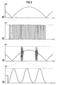
- Figur 1
- das Schaltbild einer Ausführungsform einer erfindungsgemäßen Stromversorgung und
- Figur 2
- den Verlauf ausgewählter Signale bei der Stromversorgung nach Figur 1.
Claims (10)
- Stromversorgung zur Versorgung eines Hauptstromkreises bei Normalbetrieb und eines Hilfsstromkreises bei Stand-By-Betrieb mit:einem geschalteten Leistungswandler, der zwischen eine Eingangsspannung und dem Hauptstromkreis geschaltet ist und der eine Drossel (6), einen steuerbaren Schalter (7), eine erste Gleichrichteinheit (8) sowie eine Steuereinheit (11, 12, 17, 18, 19) für den Schalter aufweist, undeiner zweiten Gleichrichteinheit (16) zur Einkopplung der über der Drossel (6) abfallenden Spannung in den Hilfsstromkreis,wobei im Stand-by-Betrieb die Steuereinheit (11, 12, 17, 18, 19) den Schalter (7) derart steuert, daß der geschaltete Leistungswandler in Resonanzmodus betrieben wird.
- Stromversorgung nach Anspruch 1, bei der im Stand-By-Betrieb die Steuereinheit (11, 12, 17, 18, 19) den Schalter (7) nur dann einschaltet, wenn die Spannung am Schalter näherungsweise Null ist.
- Stromversorgung nach Anspruch 1 oder 2, bei der zwischen Drossel (6) und zweiter Gleichrichteinheit (16) ein Kondensator (15) geschaltet ist.
- Stromversorgung nach einem der vorherigen Ansprüche, bei der die Spannung über der Drossel (6) mittels einer mit der Drossel (6) induktiv gekoppelten Hilfswicklung (14) abgenommen wird.
- Stromversorgung nach einem der vorherigen Ansprüche, bei der der Leistungswandler im Stand-By-Betrieb mit einer Frequenz betrieben wird, die im wesentlichen gleich der Resonanzfrequenz aus Drosselinduktivität und der Summe aller dazu parallel liegenden Kapazitäten ist.
- Stromversorgung nach einem der vorherigen Ansprüche, bei der im Stand-By-Betrieb der Schalter (7) durch die Steuereinheit (11, 12, 17, 18, 19) nicht eingeschaltet wird, wenn die Eingangsspannung höher ist als die Hälfte der Nennausgangsspannung des Leistungswandlers.
- Stromversorgung nach einem der vorherigen Ansprüche, bei der der geschaltete Leistungswandler ein Hochsetzsteller ist.
- Stromversorgung nach einem der vorherigen Ansprüche, bei der im Stand-By-Betrieb der Schalter (7) durch die Steuereinheit in Form einer Folge von kurzzeitigen Impulsen eingeschaltet wird.
- Stromversorgung nach Anspruch 8, bei der die Folgen von Impulsen zu Zeitpunkten erfolgen, an denen der Momentanwert der Eingangsspannung im wesentlichen halb so groß ist wie die Spannung am Hilfsstromkreis.
- Stromversorgung nach Anspruch 8 oder 9, bei der die Steuereinrichtung die Anzahl der Impulse innerhalb einer Folge in Abhängigkeit von der Spannung am Hilfsstromkreis regelt.
Applications Claiming Priority (2)
| Application Number | Priority Date | Filing Date | Title |
|---|---|---|---|
| DE19801499 | 1998-01-16 | ||
| DE19801499A DE19801499C2 (de) | 1998-01-16 | 1998-01-16 | Getaktete Stromversorgung |
Publications (2)
| Publication Number | Publication Date |
|---|---|
| EP0930690A2 true EP0930690A2 (de) | 1999-07-21 |
| EP0930690A3 EP0930690A3 (de) | 1999-11-17 |
Family
ID=7854825
Family Applications (1)
| Application Number | Title | Priority Date | Filing Date |
|---|---|---|---|
| EP99100713A Withdrawn EP0930690A3 (de) | 1998-01-16 | 1999-01-15 | Getaktete Stromversorgung |
Country Status (3)
| Country | Link |
|---|---|
| EP (1) | EP0930690A3 (de) |
| JP (1) | JP3615668B2 (de) |
| DE (1) | DE19801499C2 (de) |
Families Citing this family (2)
| Publication number | Priority date | Publication date | Assignee | Title |
|---|---|---|---|---|
| DE102006007169A1 (de) * | 2006-02-08 | 2007-08-09 | E.G.O. Elektro-Gerätebau GmbH | Vorrichtung und Verfahren zum Betrieb eines Elektrogerätes mit einer außen ansetzbaren Bedieneinrichtung |
| CN102751793B (zh) * | 2012-07-06 | 2014-08-06 | 重庆大学 | 基于双边功率流控制的无线电能传输系统及其控制方法 |
Citations (2)
| Publication number | Priority date | Publication date | Assignee | Title |
|---|---|---|---|---|
| EP0490639A2 (de) * | 1990-12-10 | 1992-06-17 | Nec Corporation | Schaltenergiequelle |
| US5691889A (en) * | 1995-12-13 | 1997-11-25 | Unitrode Corporation | Controller having feed-forward and synchronization features |
Family Cites Families (3)
| Publication number | Priority date | Publication date | Assignee | Title |
|---|---|---|---|---|
| JPH10501960A (ja) * | 1995-04-05 | 1998-02-17 | フィリップス エレクトロニクス ネムローゼ フェンノートシャップ | 切替モード電源 |
| DE19641299C2 (de) * | 1996-10-07 | 2000-08-03 | Siemens Ag | Getaktete Stromversorgung von Schaltnetzteilen |
| US5812383A (en) * | 1997-07-31 | 1998-09-22 | Philips Electronics North North America Corporation | Low power stand-by for switched-mode power supply circuit with burst mode operation |
-
1998
- 1998-01-16 DE DE19801499A patent/DE19801499C2/de not_active Expired - Fee Related
-
1999
- 1999-01-14 JP JP00793799A patent/JP3615668B2/ja not_active Expired - Fee Related
- 1999-01-15 EP EP99100713A patent/EP0930690A3/de not_active Withdrawn
Patent Citations (2)
| Publication number | Priority date | Publication date | Assignee | Title |
|---|---|---|---|---|
| EP0490639A2 (de) * | 1990-12-10 | 1992-06-17 | Nec Corporation | Schaltenergiequelle |
| US5691889A (en) * | 1995-12-13 | 1997-11-25 | Unitrode Corporation | Controller having feed-forward and synchronization features |
Also Published As
| Publication number | Publication date |
|---|---|
| DE19801499A1 (de) | 1999-07-22 |
| EP0930690A3 (de) | 1999-11-17 |
| JP3615668B2 (ja) | 2005-02-02 |
| JPH11262249A (ja) | 1999-09-24 |
| DE19801499C2 (de) | 2000-05-18 |
Similar Documents
| Publication | Publication Date | Title |
|---|---|---|
| DE69826172T2 (de) | Stromversorgungsgerät | |
| DE69632439T2 (de) | Unterbrechungsfreies Schaltreglersystem | |
| DE69400323T2 (de) | Mehrschleifensteuereinrichtung und Verfahren für Leistungsschaltwandler mit Bandpass Stromsteuerung | |
| DE2756799A1 (de) | Impulsgesteuertes stromversorgungsgeraet | |
| EP0873651B1 (de) | Schaltnetzteil mit verlustleistungsarmem standby-betrieb | |
| DE2658903A1 (de) | Schalt-spannungsregler | |
| EP0758815B1 (de) | Spannungskonverter | |
| DE10122534A1 (de) | Resonanter Konverter | |
| DE2649910B2 (de) | Versorgungsspannungsanordnung für fernsehtechnische Geräte | |
| EP1114506B1 (de) | Schaltnetzteil | |
| DE60223216T2 (de) | Kopplungseinrichtung für ein Übertragungssystem mit Trägerstrom niedriger Datenübertragungsrate | |
| EP0135119B1 (de) | Sperrwandler-Schaltnetzteil | |
| DE69410775T2 (de) | Elektronisches Vorschaltgerät für Entladungslampen mit einem Resonanzkreis zur Begrenzung des Formfaktors und zur Verbesserung des Leistungsfaktors | |
| EP0803966A2 (de) | Netzteil für ein Gerät mit Standby-Betrieb | |
| DE69836498T2 (de) | Schaltnetzteil | |
| DE2411871C2 (de) | Schaltungsanordnung zur erdfreien Übertragung von Signalen über Trennstellen in Fernmeldeanlagen | |
| WO1986005345A1 (fr) | Concept alimentation electrique-balayage pour postes de television | |
| EP0252165A1 (de) | Schaltnetzteil | |
| EP0930690A2 (de) | Getaktete Stromversorgung | |
| DE3323371C2 (de) | ||
| DE3044729A1 (de) | Horizontalablenkschaltung und stromversorgung mit regelung ueber die abschaltverzoegerung des horizontalausgangstransistors | |
| EP1283587B1 (de) | Netzgerät | |
| DE3501052A1 (de) | Wandlerschaltung | |
| DE4120147C2 (de) | ||
| DE4403731C1 (de) | Schaltnetzteil für stromsparenden Stand-by-Betrieb |
Legal Events
| Date | Code | Title | Description |
|---|---|---|---|
| PUAI | Public reference made under article 153(3) epc to a published international application that has entered the european phase |
Free format text: ORIGINAL CODE: 0009012 |
|
| AK | Designated contracting states |
Kind code of ref document: A2 Designated state(s): DE ES FR GB IE IT PT |
|
| AX | Request for extension of the european patent |
Free format text: AL;LT;LV;MK;RO;SI |
|
| PUAL | Search report despatched |
Free format text: ORIGINAL CODE: 0009013 |
|
| RIC1 | Information provided on ipc code assigned before grant |
Free format text: 6H 02J 9/06 A, 6H 02M 1/00 B, 6H 02M 3/335 B, 6H 02J 9/00 B |
|
| AK | Designated contracting states |
Kind code of ref document: A3 Designated state(s): AT BE CH CY DE DK ES FI FR GB GR IE IT LI LU MC NL PT SE |
|
| AX | Request for extension of the european patent |
Free format text: AL;LT;LV;MK;RO;SI |
|
| 17P | Request for examination filed |
Effective date: 19991206 |
|
| AKX | Designation fees paid |
Free format text: DE ES FR GB IE IT PT |
|
| RAP1 | Party data changed (applicant data changed or rights of an application transferred) |
Owner name: INFINEON TECHNOLOGIES AG |
|
| 17Q | First examination report despatched |
Effective date: 20071220 |
|
| STAA | Information on the status of an ep patent application or granted ep patent |
Free format text: STATUS: THE APPLICATION IS DEEMED TO BE WITHDRAWN |
|
| 18D | Application deemed to be withdrawn |
Effective date: 20080503 |