EP0929108A2 - Optische Übertragungs-und Empfangsvorrichtung und Herstellungsverfahren - Google Patents
Optische Übertragungs-und Empfangsvorrichtung und Herstellungsverfahren Download PDFInfo
- Publication number
- EP0929108A2 EP0929108A2 EP98114170A EP98114170A EP0929108A2 EP 0929108 A2 EP0929108 A2 EP 0929108A2 EP 98114170 A EP98114170 A EP 98114170A EP 98114170 A EP98114170 A EP 98114170A EP 0929108 A2 EP0929108 A2 EP 0929108A2
- Authority
- EP
- European Patent Office
- Prior art keywords
- receiving device
- substrate
- layer
- insulation layer
- optical transmitting
- Prior art date
- Legal status (The legal status is an assumption and is not a legal conclusion. Google has not performed a legal analysis and makes no representation as to the accuracy of the status listed.)
- Granted
Links
- 230000003287 optical effect Effects 0.000 title claims abstract description 143
- 238000004519 manufacturing process Methods 0.000 title claims description 42
- 239000000758 substrate Substances 0.000 claims abstract description 160
- 238000009413 insulation Methods 0.000 claims abstract description 74
- 239000010432 diamond Substances 0.000 claims abstract description 19
- 229910003460 diamond Inorganic materials 0.000 claims abstract description 19
- 239000010410 layer Substances 0.000 claims description 167
- 239000004065 semiconductor Substances 0.000 claims description 26
- 239000012535 impurity Substances 0.000 claims description 22
- 238000010030 laminating Methods 0.000 claims description 5
- 230000015572 biosynthetic process Effects 0.000 claims description 4
- 239000002344 surface layer Substances 0.000 claims description 4
- 239000010409 thin film Substances 0.000 claims 2
- 239000004020 conductor Substances 0.000 claims 1
- VYPSYNLAJGMNEJ-UHFFFAOYSA-N Silicium dioxide Chemical compound O=[Si]=O VYPSYNLAJGMNEJ-UHFFFAOYSA-N 0.000 abstract description 82
- 239000000377 silicon dioxide Substances 0.000 abstract description 41
- 235000012239 silicon dioxide Nutrition 0.000 abstract description 15
- 238000000034 method Methods 0.000 description 24
- 230000008569 process Effects 0.000 description 18
- 230000003071 parasitic effect Effects 0.000 description 9
- 238000005530 etching Methods 0.000 description 7
- 239000013307 optical fiber Substances 0.000 description 7
- 239000000853 adhesive Substances 0.000 description 6
- 230000001070 adhesive effect Effects 0.000 description 6
- 238000010586 diagram Methods 0.000 description 6
- 230000005540 biological transmission Effects 0.000 description 5
- 230000000694 effects Effects 0.000 description 5
- 239000010931 gold Substances 0.000 description 5
- OAICVXFJPJFONN-UHFFFAOYSA-N Phosphorus Chemical compound [P] OAICVXFJPJFONN-UHFFFAOYSA-N 0.000 description 4
- XUIMIQQOPSSXEZ-UHFFFAOYSA-N Silicon Chemical compound [Si] XUIMIQQOPSSXEZ-UHFFFAOYSA-N 0.000 description 4
- 238000004891 communication Methods 0.000 description 4
- 238000005516 engineering process Methods 0.000 description 4
- 229910052698 phosphorus Inorganic materials 0.000 description 4
- 239000011574 phosphorus Substances 0.000 description 4
- 229910052710 silicon Inorganic materials 0.000 description 4
- 239000010703 silicon Substances 0.000 description 4
- 239000000463 material Substances 0.000 description 3
- 230000007246 mechanism Effects 0.000 description 3
- 238000000206 photolithography Methods 0.000 description 3
- 238000001020 plasma etching Methods 0.000 description 3
- 230000002265 prevention Effects 0.000 description 3
- ZOXJGFHDIHLPTG-UHFFFAOYSA-N Boron Chemical compound [B] ZOXJGFHDIHLPTG-UHFFFAOYSA-N 0.000 description 2
- KRHYYFGTRYWZRS-UHFFFAOYSA-N Fluorane Chemical compound F KRHYYFGTRYWZRS-UHFFFAOYSA-N 0.000 description 2
- 230000008901 benefit Effects 0.000 description 2
- KGBXLFKZBHKPEV-UHFFFAOYSA-N boric acid Chemical compound OB(O)O KGBXLFKZBHKPEV-UHFFFAOYSA-N 0.000 description 2
- 239000004327 boric acid Substances 0.000 description 2
- 229910052796 boron Inorganic materials 0.000 description 2
- 238000004140 cleaning Methods 0.000 description 2
- 238000000151 deposition Methods 0.000 description 2
- 238000009792 diffusion process Methods 0.000 description 2
- 238000010438 heat treatment Methods 0.000 description 2
- 229960002050 hydrofluoric acid Drugs 0.000 description 2
- 230000010355 oscillation Effects 0.000 description 2
- 230000005855 radiation Effects 0.000 description 2
- 230000009467 reduction Effects 0.000 description 2
- 230000003014 reinforcing effect Effects 0.000 description 2
- 229910000679 solder Inorganic materials 0.000 description 2
- 239000000126 substance Substances 0.000 description 2
- 230000008016 vaporization Effects 0.000 description 2
- 238000009834 vaporization Methods 0.000 description 2
- 235000010627 Phaseolus vulgaris Nutrition 0.000 description 1
- 244000046052 Phaseolus vulgaris Species 0.000 description 1
- 239000004642 Polyimide Substances 0.000 description 1
- BQCADISMDOOEFD-UHFFFAOYSA-N Silver Chemical compound [Ag] BQCADISMDOOEFD-UHFFFAOYSA-N 0.000 description 1
- ATJFFYVFTNAWJD-UHFFFAOYSA-N Tin Chemical compound [Sn] ATJFFYVFTNAWJD-UHFFFAOYSA-N 0.000 description 1
- QVGXLLKOCUKJST-UHFFFAOYSA-N atomic oxygen Chemical compound [O] QVGXLLKOCUKJST-UHFFFAOYSA-N 0.000 description 1
- 238000007906 compression Methods 0.000 description 1
- 238000010276 construction Methods 0.000 description 1
- 239000013078 crystal Substances 0.000 description 1
- 239000002019 doping agent Substances 0.000 description 1
- 239000000835 fiber Substances 0.000 description 1
- PCHJSUWPFVWCPO-UHFFFAOYSA-N gold Chemical compound [Au] PCHJSUWPFVWCPO-UHFFFAOYSA-N 0.000 description 1
- 229910052737 gold Inorganic materials 0.000 description 1
- 239000011810 insulating material Substances 0.000 description 1
- GQYHUHYESMUTHG-UHFFFAOYSA-N lithium niobate Chemical compound [Li+].[O-][Nb](=O)=O GQYHUHYESMUTHG-UHFFFAOYSA-N 0.000 description 1
- 229910052760 oxygen Inorganic materials 0.000 description 1
- 239000001301 oxygen Substances 0.000 description 1
- 239000004033 plastic Substances 0.000 description 1
- 238000005498 polishing Methods 0.000 description 1
- 238000007517 polishing process Methods 0.000 description 1
- 229920001721 polyimide Polymers 0.000 description 1
- 238000012545 processing Methods 0.000 description 1
- 238000012827 research and development Methods 0.000 description 1
- 239000011347 resin Substances 0.000 description 1
- 229920005989 resin Polymers 0.000 description 1
- 229910052709 silver Inorganic materials 0.000 description 1
- 239000004332 silver Substances 0.000 description 1
- 238000003892 spreading Methods 0.000 description 1
- 230000007480 spreading Effects 0.000 description 1
- 229920001187 thermosetting polymer Polymers 0.000 description 1
- 238000012546 transfer Methods 0.000 description 1
Images


Classifications
-
- H—ELECTRICITY
- H01—ELECTRIC ELEMENTS
- H01L—SEMICONDUCTOR DEVICES NOT COVERED BY CLASS H10
- H01L31/00—Semiconductor devices sensitive to infrared radiation, light, electromagnetic radiation of shorter wavelength or corpuscular radiation and specially adapted either for the conversion of the energy of such radiation into electrical energy or for the control of electrical energy by such radiation; Processes or apparatus specially adapted for the manufacture or treatment thereof or of parts thereof; Details thereof
- H01L31/12—Semiconductor devices sensitive to infrared radiation, light, electromagnetic radiation of shorter wavelength or corpuscular radiation and specially adapted either for the conversion of the energy of such radiation into electrical energy or for the control of electrical energy by such radiation; Processes or apparatus specially adapted for the manufacture or treatment thereof or of parts thereof; Details thereof structurally associated with, e.g. formed in or on a common substrate with, one or more electric light sources, e.g. electroluminescent light sources, and electrically or optically coupled thereto
-
- G—PHYSICS
- G02—OPTICS
- G02B—OPTICAL ELEMENTS, SYSTEMS OR APPARATUS
- G02B6/00—Light guides; Structural details of arrangements comprising light guides and other optical elements, e.g. couplings
- G02B6/24—Coupling light guides
- G02B6/42—Coupling light guides with opto-electronic elements
- G02B6/4201—Packages, e.g. shape, construction, internal or external details
- G02B6/4246—Bidirectionally operating package structures
-
- H—ELECTRICITY
- H01—ELECTRIC ELEMENTS
- H01L—SEMICONDUCTOR DEVICES NOT COVERED BY CLASS H10
- H01L2224/00—Indexing scheme for arrangements for connecting or disconnecting semiconductor or solid-state bodies and methods related thereto as covered by H01L24/00
- H01L2224/01—Means for bonding being attached to, or being formed on, the surface to be connected, e.g. chip-to-package, die-attach, "first-level" interconnects; Manufacturing methods related thereto
- H01L2224/42—Wire connectors; Manufacturing methods related thereto
- H01L2224/44—Structure, shape, material or disposition of the wire connectors prior to the connecting process
- H01L2224/45—Structure, shape, material or disposition of the wire connectors prior to the connecting process of an individual wire connector
- H01L2224/45001—Core members of the connector
- H01L2224/45099—Material
- H01L2224/451—Material with a principal constituent of the material being a metal or a metalloid, e.g. boron (B), silicon (Si), germanium (Ge), arsenic (As), antimony (Sb), tellurium (Te) and polonium (Po), and alloys thereof
- H01L2224/45138—Material with a principal constituent of the material being a metal or a metalloid, e.g. boron (B), silicon (Si), germanium (Ge), arsenic (As), antimony (Sb), tellurium (Te) and polonium (Po), and alloys thereof the principal constituent melting at a temperature of greater than or equal to 950°C and less than 1550°C
- H01L2224/45144—Gold (Au) as principal constituent
-
- H—ELECTRICITY
- H01—ELECTRIC ELEMENTS
- H01L—SEMICONDUCTOR DEVICES NOT COVERED BY CLASS H10
- H01L2224/00—Indexing scheme for arrangements for connecting or disconnecting semiconductor or solid-state bodies and methods related thereto as covered by H01L24/00
- H01L2224/01—Means for bonding being attached to, or being formed on, the surface to be connected, e.g. chip-to-package, die-attach, "first-level" interconnects; Manufacturing methods related thereto
- H01L2224/42—Wire connectors; Manufacturing methods related thereto
- H01L2224/47—Structure, shape, material or disposition of the wire connectors after the connecting process
- H01L2224/48—Structure, shape, material or disposition of the wire connectors after the connecting process of an individual wire connector
- H01L2224/4805—Shape
- H01L2224/4809—Loop shape
- H01L2224/48091—Arched
-
- H—ELECTRICITY
- H01—ELECTRIC ELEMENTS
- H01L—SEMICONDUCTOR DEVICES NOT COVERED BY CLASS H10
- H01L25/00—Assemblies consisting of a plurality of individual semiconductor or other solid state devices ; Multistep manufacturing processes thereof
- H01L25/16—Assemblies consisting of a plurality of individual semiconductor or other solid state devices ; Multistep manufacturing processes thereof the devices being of types provided for in two or more different main groups of groups H01L27/00 - H01L33/00, or in a single subclass of H10K, H10N, e.g. forming hybrid circuits
- H01L25/167—Assemblies consisting of a plurality of individual semiconductor or other solid state devices ; Multistep manufacturing processes thereof the devices being of types provided for in two or more different main groups of groups H01L27/00 - H01L33/00, or in a single subclass of H10K, H10N, e.g. forming hybrid circuits comprising optoelectronic devices, e.g. LED, photodiodes
-
- H—ELECTRICITY
- H01—ELECTRIC ELEMENTS
- H01L—SEMICONDUCTOR DEVICES NOT COVERED BY CLASS H10
- H01L2924/00—Indexing scheme for arrangements or methods for connecting or disconnecting semiconductor or solid-state bodies as covered by H01L24/00
- H01L2924/30—Technical effects
- H01L2924/301—Electrical effects
- H01L2924/3011—Impedance
-
- H—ELECTRICITY
- H01—ELECTRIC ELEMENTS
- H01L—SEMICONDUCTOR DEVICES NOT COVERED BY CLASS H10
- H01L2924/00—Indexing scheme for arrangements or methods for connecting or disconnecting semiconductor or solid-state bodies as covered by H01L24/00
- H01L2924/30—Technical effects
- H01L2924/301—Electrical effects
- H01L2924/3025—Electromagnetic shielding
-
- H—ELECTRICITY
- H01—ELECTRIC ELEMENTS
- H01S—DEVICES USING THE PROCESS OF LIGHT AMPLIFICATION BY STIMULATED EMISSION OF RADIATION [LASER] TO AMPLIFY OR GENERATE LIGHT; DEVICES USING STIMULATED EMISSION OF ELECTROMAGNETIC RADIATION IN WAVE RANGES OTHER THAN OPTICAL
- H01S5/00—Semiconductor lasers
- H01S5/005—Optical components external to the laser cavity, specially adapted therefor, e.g. for homogenisation or merging of the beams or for manipulating laser pulses, e.g. pulse shaping
- H01S5/0085—Optical components external to the laser cavity, specially adapted therefor, e.g. for homogenisation or merging of the beams or for manipulating laser pulses, e.g. pulse shaping for modulating the output, i.e. the laser beam is modulated outside the laser cavity
-
- H—ELECTRICITY
- H01—ELECTRIC ELEMENTS
- H01S—DEVICES USING THE PROCESS OF LIGHT AMPLIFICATION BY STIMULATED EMISSION OF RADIATION [LASER] TO AMPLIFY OR GENERATE LIGHT; DEVICES USING STIMULATED EMISSION OF ELECTROMAGNETIC RADIATION IN WAVE RANGES OTHER THAN OPTICAL
- H01S5/00—Semiconductor lasers
- H01S5/02—Structural details or components not essential to laser action
- H01S5/022—Mountings; Housings
- H01S5/023—Mount members, e.g. sub-mount members
- H01S5/02325—Mechanically integrated components on mount members or optical micro-benches
Definitions
- the present invention relates to an optical transmitting and receiving device incorporating a light emitting device (LED) and a light receiving device into a substrate.
- LED light emitting device
- trunk route communication networks have been formed using optical fibers, and channels laid from trunk route networks to subscribers, that is, subscriber channels, still remain as electrical circuits.
- subscriber channels To further spread the use of optical communication networks, it is desired that all the subscriber channels also consist of optical channels. To meet this expectation a variety of research and development is actively being carried out.
- optical devices including a WDM filter constitutes a very important factor in the construction of an optical subscriber system using a wavelength multiplex technology called an "ATM-PON (Asynchronous Transfer Mode-Passive Optical Network).
- ATM-PON Asynchronous Transfer Mode-Passive Optical Network
- the mounting of a small number of compact optical devices is indispensable, and a device form in which an LED, a light receiving device and a WDM filter are hybrid-mounted on a substrate is expected to be developed.
- the transmitting unit and receiving unit of a optical module operate asychronously in the ATM-PON system, it is necessary that the crosstalk between transmission and reception in the module is sufficiently small.
- Fig .1 explains the configuration of a conventional optical transmitting and receiving device.
- an LED 1004 and a light receiving device 1005 and a WDM filter 1002 are encapsulated as discrete devices, and the devices are connected to an optical network and with each other using optical fibers 1001 and 1003, respectively.
- the CAN packages of the LED 1004 and the light receiving device 1005 are utilized as electrostatic shielding to suppress the crosstalk between transmission and reception signals.
- Fig.2 explains how crosstalk is generated between an LED and a light receiving device in a hybrid-mounted optical transmitting and receiving device.
- a silicon dioxide film (SiO 2 ) 1104 is formed on a silicon (Si) substrate 1106, and on the silicon dioxide film electrodes 1102 and 1103 are formed. Then, the electrodes 1102 and 1103 are connected to the LD 1100 and PD 1101, respectively.
- a metallic film (not shown in the diagram) is provided to ground the back of the substrate 1106.
- the silicon dioxide film 1104 is provided so that current may not flow in the electrode 1103 of the PD 1101 due to the voltage generated by the electrode 1102, current leaks to the substrate 1106 by the effect of alternating voltage applied to LD 1100 since the insulation function of the silicon dioxide film 1104 is not complete and the silicon dioxide film 1104 itself has its own capacitance. At this moment, although much of the current flows out of the substrate 1106 since the back of the substrate 1106 is grounded, part of the current reaches the electrode 1103 through the inside of the substrate 1106.
- the silicon dioxide film 1105 is a heat-oxidized film generated during the substrate processing, and if the back of the substrate 1106 is left unprocessed, the thickness of this silicon dioxide film 1105 will grow to approximately 2 ⁇ m.
- the crosstalk between the transmitting side and the receiving side is roughly classified into two groups; crosstalk due to an optical cause such as stray light, etc., and crosstalk due to an electrical cause such as free capacitance, etc.
- the electrical cause is generated by a current flowing between the transmitting side and receiving side through the substrate, and this is a serious problem.
- the stray light, etc. is generated by light beams emitted from the LD leaking out from an optical waveguide and generating a mode spreading over all the substrate. Accordingly, when the PD receives such stray light, it becomes impossible to accurately receive optical signals.
- the optical transmitting and receiving device of the present invention comprises a conduction layer formed on all or a part of the surface of a substrate, an insulation layer formed at least at the bottom of an LED mounting portion and a light receiving device mounting portion, an optical waveguide formed on the surface of the insulation layer, electric wiring patterns formed on the surface of the insulation layer, and an LED and a light receiving device connected to the electric wiring patterns so as to be optically coupled with the optical waveguide.
- the optical transmitting and receiving device is characterized in that the above-mentioned conduction layer is made electrically connectable to a constant potential portion.
- the manufacturing method of the optical transmitting and receiving device of the present invention comprises the steps of forming a conduction layer by doping an impurity on the surface of the substrate, laminating an insulation layer on the surface of the conduction layer, providing an optical waveguide on the insulation layer and mounting an LED and a light receiving device.
- the optical transmitting and receiving device in another aspect of the present invention is characterized in that in an optical transmitting and receiving device hybrid-mounting at least an LED and a light receiving device on the same substrate through the insulation layer, a conduction layer is located at least at the bottom of the above-mentioned LED and the above-mentioned light receiving device, and between the above-mentioned substrate and the above-mentioned insulation layer, and the conduction layer can be electrically connected to a constant potential portion.
- the optical transmitting and receiving device in another aspect of the present invention is characterized in that in an optical transmitting and receiving device hybrid-mounting at least an LED and a light receiving device on the same substrate through the insulation layer, the above-mentioned substrate is a semiconductor substrate of one (p or n type) conduction type, and a semiconductor layer of one (n or p type) conduction type the reverse of the above-mentioned (p or n type) conduction type, forming a pn junction together with the above-mentioned semiconductor substrate, and is located at least at the bottom of the above-mentioned LED and the above-mentioned light receiving device and between the above-mentioned semiconductor substrate and the above-mentioned insulation layer, and the voltage applied between the above-mentioned LED and a light receiving device, and the back of the above-mentioned semiconductor substrate is biased the reverse of the above-mentioned pn junction.
- the manufacturing method of the optical transmitting and receiving device in another aspect of the present invention is characterized in that in the manufacturing method of an optical transmitting and receiving device hybrid-mounting at least an LED and a light receiving device on the same substrate through the insulation layer, comprises a process for forming a conduction layer electrically connectable to the constant potential portion on the surface layer portion of the above-mentioned substrate and at the bottom of at least the above-mentioned LED mounting portion and the above-mentioned light receiving device mounting portion, prior to the formation of the above-mentioned insulation layer.
- the manufacturing method of the optical transmitting and receiving device in another aspect of the present invention is characterized in that in the manufacturing method of an optical transmitting and receiving device hybrid-mounting at least an LED and a light receiving device on the same substrate through the insulation layer, comprises a process for forming a conduction layer of one (n or p type) conduction type the reverse of the above-mentioned (p or n type) conduction type, forming a pn junction together with the above-mentioned semiconductor substrate, on the surface layer portion of the above-mentioned substrate and at the bottom of a portion mounting at least the above-mentioned LED and the above-mentioned light receiving device, prior to the formation of the above-mentioned insulation layer using a semiconductor substrate of one (p or n type) conduction type for the above-mentioned substrate.
- the platform of the optical transmitting and receiving device of the present invention comprises a conduction layer formed on all or a part of the surface of the substrate, an insulation layer formed at the bottom of portions mounting at least an LED and a light receiving device, an optical waveguide formed on the surface of the insulation layer, and an electric wiring pattern formed on the surface of the insulation layer, and is characterized in that the above-mentioned conduction layer can be electrically connected to a constant potential portion.
- the manufacturing method of the platform of the optical transmitting and receiving device of the present invention comprises the steps of forming a conduction layer by doping an impurity on the surface of the substrate, laminating an insulation layer on the surface of the conduction layer, providing an optical waveguide on the surface of the insulation layer, and forming an electric wiring pattern on the surface of the insulation layer.
- an optical transmitting and receiving device of the present invention since the current leaking from the LED to the substrate through the conduction layer can be eliminated, no current leaks to the light receiving device side. Accordingly, the crosstalk between the transmitting side and the receiving side can be suppressed, the transmission side and the receiving side can be simultaneously operated, and thereby a miniature hybrid-mounted optical transmitting and receiving device required to construct a subscriber system in an optical communication network using an optical circuit can be provided.
- Figs.3A and 3B show an example of a hybrid-mounted optical device using a PLC platform according to the present invention.
- a platform substrate 11 is, for example, a silicon substrate, and an insulation film 18 is formed on the substrate.
- the insulation film 18 is made of SiO 2 , etc.
- an LED 12, a light receiving device 16 and an overclad 19, excluding a transmitting unit wiring pattern 13 and a receiving unit wiring pattern 17, is provided on the surface of this insulation layer 18. Accordingly, the insulation film 18 becomes the underclad of a waveguide 14.
- the overclad 19 is made of SiO 2 or the same substance as the insulation film, such as lithium niobate, etc. Then, a waveguide 14 for guiding light beams between the overclad 19 and the underclad is formed.
- the waveguide 14 is structured so as to guide light beams from the LED 12 to a WDM filter 15 provided in a groove in the overclad 19, and to guide optical signals transmitted and reflected by the WDM filter 15 to the light receiving device 16 and a light entrance/exit 20, respectively.
- the LED 12 is provided on the side of the WDM filter 15 where there is the entrance/exit 20 of the waveguide 14, and the light receiving device 16 is provided on the opposite side of the WDM filter.
- the LED 12 is driven by the current supplied from the transmitting unit wiring pattern 13, and the light receiving device 16 outputs electric signals corresponding to received optical signals to the receiving unit wiring pattern 17.
- Fig.3B shows the operation of the optical transmitting and receiving device shown in Fig.3A.
- the LED 12 transmits optical signals of a first wavelength (for example, 1.3 ⁇ m) to the waveguide 14.
- the WDM filter 15 is designed so as to reflect the optical signals of the first wavelength.
- the optical signals reflected by the WDM filter are outputted from the entrance/exit 20 of the waveguide 14.
- optical signals of a second wavelength (for example, 1.55 ⁇ m) different from the first wavelength are used for signals received from the entrance/exit 20.
- the WDM filter 15 is designed to transmit optical signals of the second wavelength.
- the optical signals of the second wavelength received from the entrance/exit 20 pass through the WDM filter, and are received by the light receiving device 16.
- an optical transmitting and receiving device hybrid-mounting a transmitting unit and a receiving unit can be configured by using different wavelengths for outgoing and incoming optical signals.
- the LED 12 is provided on the entrance/exit 20 side of the WDM filter 15. This is because when outgoing optical signals outputted from the LED 12 or incoming optical signals received from the entrance/exit 20 leak out from the waveguide 14, and an oscillation mode is generated over all the overclad 19 and underclad (insulation layer 18), this oscillation mode over all the overclad 19 and underclad is stray light which can be isolated by the WDM filter 15 to prevent the stray light from entering the light receiving device 16.
- crosstalk between the transmitting and receiving sides due to stray light can be suppressed to a minimum.
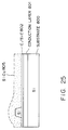
- Figs.4 and 5 explain the electrical crosstalk generating mechanism of a hybrid optical transmitting and receiving device shown in Figs.3A and 3B and the prevention method.
- Fig.4 is the cross sectional diagram of the optical transmitting and receiving device, and shows that there is parasitic capacitance.
- Fig.5 shows the equivalent circuit model.
- parasitic capacitances C 12 and C 34 are generated in the transmitting unit wiring pattern 13 and the receiving unit wiring pattern 17, respectively. Since the parasitic capacitance does not form a route from the LED 12 to the light receiving device 16 as shown in the equivalent circuit of Fig.5, this parasitic capacitance has no effect on crosstalk between the transmitting side and the receiving side.
- the impedance value of the parasitic capacitance C SG possessed by a silicon dioxide film 21 plays a role of determining whether the current from the LED should flow to ground or to the light receiving device 16 as shown in the equivalent circuit of Fig.5, the capacitance C SG becomes an important factor in the reduction of the electrical crosstalk.
- Crosstalk is generated between the transmitting side and the receiving side since the driving current of the LED 12 leaks from the transmitting unit wiring pattern 13 to the receiving unit wiring pattern 17 via series capacitance (C 1S , C 2S , C 3S or C 4S in Fig.4 or Fig.5) formed between the transmitting unit wiring pattern 13 and the platform substrate 11 and between the receiving unit wiring pattern 17 and the platform substrate 11.
- series capacitance C 1S , C 2S , C 3S or C 4S in Fig.4 or Fig.5
- the branching ratio of the current is determined by the ratio of the reciprocal of the impedance, it is necessary to increase the impedance (1/j ⁇ C 1S , 1/j ⁇ C 2S , 1/j ⁇ C 3S and 1/j ⁇ C 4S ) on the side connected to the receiving unit at each branching point and to reduce the impedance on the side not connected to the receiving unit (1/j ⁇ C SG ) at each branching point in order to reduce the current leaking to the receiving unit.
- the impedance of the route for crosstalk is increased by increasing the impedance between the transmitting unit wiring pattern 13 and the substrate 11, and the impedance between the receiving unit wiring pattern 17 and the substrate 11.
- the crosstalk current leaking to the substrate 11 is grounded by connecting the substrate 11 to a constant potential portion such as ground, etc.
- silicon is used for the substrate.
- the use of an Si substrate has advantages, such as being capable of accurately forming guiding grooves for optical fibers, ferrule, etc. using anisotropic etching, inexpensive material cost, etc.
- Ti (0.1 ⁇ m), Ni (0.1 ⁇ m) and Au (1 ⁇ m) are vaporized on the back of the Si substrate 301 as a back metallic film 302. This is needed to electrically connect the Si substrate to a constant potential portion such as ground, etc. and to make the substrate play a role in electrostatic shielding.
- the back metallic film 302 may be vaporized over all the back of the substrate, or only over the portions used for the devices.
- resist 303 is applied to optical device mounting portions 305 and 306 on the surface of the Si substrate 301 using a photo lithography technology, and the other portions of the surface of the Si substrate 301 are etched approximately 20 ⁇ m deep using a KOH solution, etc.
- the metallic film is prevented from being etched by using a resist 304.
- convex portions 305 and 306 are formed at the optical device mounting portions of the Si substrate.
- an n type impurity such as boric acid, etc. and a p type impurity such as phosphorus, etc. are doped on the surface of the substrate 301, for example, using a vapor diffusion method, etc. to form a conduction layer 307.
- SiO 2 layer 303 is applied to optical device mounting portions 305 and 306 on the surface of the Si substrate 301 using a photo lithography technology, and the other portions of the surface of the Si substrate 301 are etched approximately 20 ⁇ m deep using a KOH solution, etc.
- convex portions 305 and 306 are formed at the optical device mounting portions of the Si substrate.
- Ti (0.1 ⁇ m), Ni (0.1 ⁇ m) and Au (1 ⁇ m) are vaporized on the back of the Si substrate 301 as a back metallic film 302. This is needed to electrically connect the Si substrate to a constant potential portion such as ground, etc. and to make the substrate play a role in electrostatic shielding.
- the back metallic film 302 may be vaporized over all the back of the substrate, or only over the portions used for the devices.
- an n type impurity such as boric acid, etc. and a p type impurity such as phosphorus, etc. are doped on the surface of the substrate 301, for example, using a vapor diffusion method, etc. to form a conduction layer 307.
- an SiO 2 layer 308 over 30 ⁇ m thick is deposited using a flame deposition method, etc., and the surface of the SiO 2 layer 308 is leveled by polishing.
- an SiO 2 film 1 ⁇ m thick is left above the convex portions 305 and 306 for mounting the optical devices, particularly on the LED mounting portion 305 which generates a lot of heat.
- the substrate can be polished until the Si substrate of the optical device mounting portions 305 and 306 is exposed, and after that a new SiO 2 film approximately 1 ⁇ m thick can be formed again.
- the SiO 2 layer 308 formed in the process shown in Fig.12 becomes the underclad of the optical waveguide and the insulation layer between the electric wiring patterns and the Si substrate.
- a core 309 of the waveguide and an overclad 310 are formed in succession, and the waveguide ends 309a are formed on the optical device mounting portion sides.
- SiO 2 layer doped with Ge, Ti, etc. is laminated approximately 8 ⁇ m thick, portions to be left as a core 309 are covered with resist (not shown in the diagram), and the SiO 2 layer is etched using RIE (Reactive Ion Etching) with this resist as a mask until the underclad 308 is exposed.
- RIE Reactive Ion Etching
- an SiO 2 layer is laminated approximately 30 ⁇ m thick, and portions other than the optical device mounting portions 305 and 306 are covered with resist 311.
- the SiO 2 layer to be the optical device mounting portions is etched using RIE until the SiO 2 layer on the Si substrate convex portions of the optical device mounting portions 305 and 306 formed in the process shown in Fig.12 becomes approximately 1 ⁇ m thick.
- a heat-oxidized film approximately 1 ⁇ m thick can be formed.
- contact holes 323 to the conduction layer 307 are provided in the optical device mounting portions.
- electric wiring patterns 312 are formed using a lift-off method.
- resist 313 is applied over all the surface of the substrate approximately 2 ⁇ m thick (the resist must be thicker than the electric wiring patterns 314 to be formed), and the resist 313 of portions to be patterned is removed. Then, for example, Ti (0.1 ⁇ m), Ni (0.1 ⁇ m) and Au (1 ⁇ m) 314 are vaporized over the surface of the substrate in that order, and surplus vaporized metallic films are removed together with the resist 313.
- Solder bumps made of gold, tin, etc. can also be formed in the optical device mounting portions using a lift-off method in the same way as described above, if necessary.
- Aligning markers 316 can also be formed in the optical device mounting portions simultaneously with the electric wiring patterns 314, and optical elements can be aligned by referring to these markers when mounting the devices.
- a groove 317 for inserting a multilayer film filter is formed using a dicing saw, and the Si substrate 301 is cut into individual platforms.
- the groove 317 is formed so as to cross the point where an optical waveguide is branched, and the depth is equal to or greater than the depth of the provided underclad.
- optical devices 318 and 319 are aligned by referring to the aligning markers formed in the optical device mounting portions, as described above, and the optical devices 318 and 319 are installed onto the electric wiring patterns 312 by heating the platform.
- a multilayer film filter 320 is inserted, and is fixed using a light-transmitting adhesive 321.
- the optical devices 318 and 319 are mounted using a AuSn solder bumps 315 (Fig.14) formed on the electric wiring patterns 312, and then the light receiving device 319 is mounted using a conductive adhesive.
- the optical devices and the electric wiring patterns are connected with each other using wires 322.
- conduction layer pads 324 are provided.
- the conduction layer pads 324 are electrically connected to the conduction layer 307 through the contact holes 323, and the pads 324 are further connected to the terminals of the package later.
- a platform 326 is fixed to a package 325, the electric wiring patterns 312 of the platform, the conduction layer pads 324 (Fig.16) and the terminals 327 of the package 325 are connected with each other using Au wires 329.
- the metallic film 302 at the back of the substrate and the radiation pads (at the bottom of the platform 326) are stuck together using a conductive adhesive such as silver paste, etc.
- the cores of optical fiber 331 are aligned to the optical waveguide, and the optical fibers are connected using a thermosetting adhesive, UV-hardening adhesive, etc.
- the platform is encapsulated using a resin 332, etc.
- the electrical crosstalk can also be reduced by improving the insulation state between the electric wiring pattern 312 connected to the LED 318 or the light receiving device 319, etc. and the substrate 301, by leaving the SiO 2 layer underneath the LED 318 and the light receiving device 319 rather thick and forming a heat-oxidized film.
- Figs.19 and 21 explain another embodiment of the present invention.
- a thick insulation layer can be formed at the bottom of the light receiving device mounting portion 45 in the process shown in Fig.12.
- the insulation layer at the bottom of the light receiving device is thick, thereby more effective insulation can be obtained.
- a back protection resist 44 provided so as to cover the back metallic film 43 shown in Fig.19, is provided to prevent the back metallic film 43 from being etched when etching the Si substrate 46.
- etching for example, the above-mentioned KOH is used.
- a thick insulation layer can be formed at the bottom of the light receiving device mounting portion 45 in the process shown in Fig.12.
- the insulation layer at the bottom of the light receiving device is thick, thereby more effective insulation can be obtained.
- the back metallic film is vaporized on the back of the substrate.
- a conduction layer is formed over all the surface of the substrate 56, as shown in the process shown in Fig.8, as shown in Fig.21, there is no need to form a conduction layer over all the surface of the substrate 56 when a contact hole for grounding is provided in the light receiving device mounting portion 55 and the LED mounting portion 54. In this case, it is sufficient if the conduction layer is formed only in the light receiving device mounting portion 55 and the LED mounting portion 54.
- a conduction layer 51 is selectively formed only on the LED mounting portion 54 and the light receiving device mounting portion 55.
- the conduction layer is formed, for example, by doping the substrate 56 with boron, etc.
- the conduction layer is formed, for example, by doping the substrate 56 with phosphorus, etc.
- an impurity is doped after a mask layer 52 made of SiO 2 is formed using a photo lithography technology. That is, doping is performed using boron or phosphorus.
- a pn junction can be formed at the optical device mounting portions 54 and 55 by doping the substrate 56 with an impurity the reverse of the conduction type of the substrate 56. That is, if the substrate 56 is p type Si, the conduction type of both the LED mounting portion 54 and the light receiving device mounting portion 55 is made n type. When the voltage generated in the LED mounting portion 54 and the light receiving device mounting portion 55 is higher than ground, this configuration is effective. Because by making the conduction type of both the LED mounting portion 54 and the light receiving device mounting portion 55 n type, the pn junction is reversely biased by the voltage applied between the back of the substrate 56 and the optical device mounting portions, and it becomes difficult for current to flow through the pn junction.
- n type Si is used for the substrate 56, and the conduction type of both the LED mounting portion 54 and the light receiving device mounting portion 55 is made p type.
- the pn junction is reverse-biased by the voltage applied between the back of the substrate 56, and the LED mounting portion 54 and the light receiving device mounting portion 55, the current flowing through this pn junction can be eliminated. Accordingly, the current from the LED provided in the LED mounting portion 54 can be prevented from flowing as crosstalk into the light receiving device provided in the light receiving device mounting portion 55 through the substrate 56. In this way, since the crosstalk can be prevented by applying a reverse bias to the pn junction, there is no need of a configuration for connecting the conduction layer 307 to a constant potential, as required in the previous embodiment.
- both sides of the substrate can also be doped in the process shown in Fig.7.
- the process can also be arranged so that the conduction layer is left only on the convex surface of the optical device mounting portions on the surface of the substrate in the etching process shown in Fig.7.
- a crosstalk route is made to have a high impedance by utilizing the inverse direction characteristic of the pn junction or increasing the resistance at the bottom of the optical device mounting portions of the substrate.
- signals of the LED leaked to the substrate are grounded, etc. through a low resistance layer (conduction layer) formed beneath the insulation film 18 shown in Fig.3A.
- the crosstalk from the LED to the light receiving device can be reduced.
- low crosstalk can be realized in a miniature optical transmitting and receiving device hybrid-mounting an LED and a light receiving device, and thereby a miniature optical transmitting and receiving device for an ATM-PON can be implemented.
- a layer made of a plastic waveguide material such as polyimide, etc. can also be formed instead of the SiO 2 layer formed above.
- Using an insulating material such as heat-conductive SiC, diamond, etc. has an advantage that the heat radiation of an LED generating a lot of heat can be secured even if a thick insulation layer is used to reduce the parasitic capacitance of the LED mounting electrodes.
- Figs.22 through 29 show an embodiment in the case where SiC or a diamond layer are formed at the bottom of an LED mounting portion or a light receiving device mounting portion and the manufacturing method.
- a dopant is applied to the top of an Si substrate 800, and a conduction layer 801 is formed.
- a diamond or SiC layer 802 is formed on the conduction layer 801.
- resist 803 is applied to the layer 802 except for the LED mounting portion, and Si is selectively grown.
- the Si does not have to be a single crystal, but can be polycrystalline.
- a Si base is formed at the LED mounting portion. This base is used later to form a waveguide, and is also used to align the LED since high accuracy is required in the alignment of the LED.
- a SiO 2 layer 805 to be used for an insulation layer is formed using a flame deposition method, etc., and as shown in Fig.26, the top of the SiO 2 layer 805 is polished and leveled until a base for the LED mounting portion appears.
- Another SiO 2 layer 806 is laminated. This layer later becomes an underclad.
- a layer 807 to be used for a waveguide of which the refractive index is greater than the refractive index of the SiO 2 layer 806 is laminated on this.
- the waveguide is formed by laminating a substance to be used for a waveguide over all the surface of the SiO 2 layer 806, and then etching the layer after applying resist to a portion to be used for a waveguide.
- Another SiO 2 layer 808 is further laminated on the waveguide formed in this manner. This later becomes an overclad.
- portions to be used for a waveguide are left as they are, and portions where the LED LD and the light receiving device PD are to be provided later are etched.
- the etching shall be so deep that the top of the base for the LED mounting portion may appear.
- the top of the base for mounting the LED LD is oxidized by heating in an atmosphere of oxygen and steam, and electrodes 812 are formed on and adjacent to the top of the base.
- electrodes 811 are provided on the SiO 2 layer 805.
- a groove is formed using a dicing saw 813 in a portion where a waveguide is branched in order to insert a multilayer film filter (WDM filter).
- WDM filter multilayer film filter
- a multilayer film filter 817 is inserted in the groove formed using the dicing saw 813 and fixed using a light transmitting adhesive, and the LED 814 and light receiving device 815 are mounted and aligned.
- the metallic film is formed at the back of the substrate 800 as described above, the metallic film is omitted in these diagrams. Then, the potential of the substrate 800 is set to ground potential by grounding the metallic film.
- the bottom of the light receiving device 815 is an underclad 810, which is used as an insulation film. Particularly, since there is no base at the bottom of the light receiving device 815, and the insulation layer is thick, the inflow of current from the light transmitting element 814 can be effectively prevented.
- the conduction layer 801 is directly grounded, in this embodiment the conduction layer 801 is not directly grounded. This is because the conduction layer 801 is substantially grounded by grounding the back of the substrate 800, since it is difficult to provide a diamond layer or SiC layer with a contact hole. Since the substrate 800 is made of Si, the diamond layer or SiC layer has a high electrical conductivity, and the current easily flows from the conduction layer 801 to the back side of the substrate 800, even if only the back side of the substrate 800 is grounded. Accordingly, almost the same effect as the case where the conduction layer 801 is directly grounded can be obtained.
- a means for reducing the crosstalk between the hybrid-mounted LED and light receiving device can be provided. Accordingly, a compact optical device capable of simultaneously transmitting and receiving can be provided, and greatly contributes to the spread of optical subscriber systems.
Applications Claiming Priority (2)
| Application Number | Priority Date | Filing Date | Title |
|---|---|---|---|
| JP10002024A JPH11202140A (ja) | 1998-01-08 | 1998-01-08 | 光送受信デバイス及びその製造方法 |
| JP202498 | 1998-01-08 |
Publications (3)
| Publication Number | Publication Date |
|---|---|
| EP0929108A2 true EP0929108A2 (de) | 1999-07-14 |
| EP0929108A3 EP0929108A3 (de) | 2002-09-18 |
| EP0929108B1 EP0929108B1 (de) | 2008-08-06 |
Family
ID=11517774
Family Applications (1)
| Application Number | Title | Priority Date | Filing Date |
|---|---|---|---|
| EP98114170A Expired - Lifetime EP0929108B1 (de) | 1998-01-08 | 1998-07-29 | Optische Übertragungs-und Empfangsvorrichtung und Herstellungsverfahren |
Country Status (4)
| Country | Link |
|---|---|
| US (2) | US6552366B1 (de) |
| EP (1) | EP0929108B1 (de) |
| JP (1) | JPH11202140A (de) |
| DE (1) | DE69839838D1 (de) |
Cited By (2)
| Publication number | Priority date | Publication date | Assignee | Title |
|---|---|---|---|---|
| JP2014127684A (ja) * | 2012-12-27 | 2014-07-07 | Kyocera Corp | 受発光素子およびこれを用いたセンサ装置 |
| US9910218B2 (en) | 2013-06-24 | 2018-03-06 | Huawei Technologies Co., Ltd. | Optical module and optical network system |
Families Citing this family (32)
| Publication number | Priority date | Publication date | Assignee | Title |
|---|---|---|---|---|
| JPH11352341A (ja) | 1998-06-04 | 1999-12-24 | Nec Corp | 導波路型波長多重光送受信モジュール |
| JP2001210841A (ja) * | 2000-01-24 | 2001-08-03 | Sumitomo Electric Ind Ltd | 光通信装置 |
| US6555890B2 (en) * | 2000-05-23 | 2003-04-29 | Sensors Unlimited, Inc. | Method for combined fabrication of indium gallium arsenide/indium phosphide avalanche photodiodes and p-i-n photodiodes |
| JP2003255195A (ja) | 2002-02-27 | 2003-09-10 | Sumitomo Electric Ind Ltd | 波長多重コネクタ、光通信装置および光通信システム |
| JP2004004459A (ja) * | 2002-04-09 | 2004-01-08 | Matsushita Electric Ind Co Ltd | 光送受信装置 |
| JP3838164B2 (ja) | 2002-06-18 | 2006-10-25 | 住友電気工業株式会社 | 光通信用素子と光通信用素子の製造方法 |
| US7189589B2 (en) * | 2002-12-20 | 2007-03-13 | Novalux, Inc. | Method of fabrication of a support structure for a semiconductor device |
| KR20050025387A (ko) * | 2003-09-06 | 2005-03-14 | 한국전자통신연구원 | 전기적 혼신이 감소된 광송수신기 |
| US7403676B2 (en) | 2004-06-09 | 2008-07-22 | Nec Corporation | Optical waveguide module |
| CA2592055A1 (en) * | 2004-12-27 | 2006-07-06 | Quantum Paper, Inc. | Addressable and printable emissive display |
| WO2007114384A1 (ja) * | 2006-04-03 | 2007-10-11 | The University Of Tokyo | 信号伝送機器 |
| US8674593B2 (en) | 2007-05-31 | 2014-03-18 | Nthdegree Technologies Worldwide Inc | Diode for a printable composition |
| US8852467B2 (en) | 2007-05-31 | 2014-10-07 | Nthdegree Technologies Worldwide Inc | Method of manufacturing a printable composition of a liquid or gel suspension of diodes |
| US8846457B2 (en) | 2007-05-31 | 2014-09-30 | Nthdegree Technologies Worldwide Inc | Printable composition of a liquid or gel suspension of diodes |
| US8877101B2 (en) | 2007-05-31 | 2014-11-04 | Nthdegree Technologies Worldwide Inc | Method of manufacturing a light emitting, power generating or other electronic apparatus |
| US8415879B2 (en) | 2007-05-31 | 2013-04-09 | Nthdegree Technologies Worldwide Inc | Diode for a printable composition |
| US8889216B2 (en) * | 2007-05-31 | 2014-11-18 | Nthdegree Technologies Worldwide Inc | Method of manufacturing addressable and static electronic displays |
| US8809126B2 (en) | 2007-05-31 | 2014-08-19 | Nthdegree Technologies Worldwide Inc | Printable composition of a liquid or gel suspension of diodes |
| US8456393B2 (en) | 2007-05-31 | 2013-06-04 | Nthdegree Technologies Worldwide Inc | Method of manufacturing a light emitting, photovoltaic or other electronic apparatus and system |
| US9018833B2 (en) | 2007-05-31 | 2015-04-28 | Nthdegree Technologies Worldwide Inc | Apparatus with light emitting or absorbing diodes |
| US9343593B2 (en) | 2007-05-31 | 2016-05-17 | Nthdegree Technologies Worldwide Inc | Printable composition of a liquid or gel suspension of diodes |
| US9425357B2 (en) | 2007-05-31 | 2016-08-23 | Nthdegree Technologies Worldwide Inc. | Diode for a printable composition |
| US9419179B2 (en) | 2007-05-31 | 2016-08-16 | Nthdegree Technologies Worldwide Inc | Diode for a printable composition |
| US8133768B2 (en) * | 2007-05-31 | 2012-03-13 | Nthdegree Technologies Worldwide Inc | Method of manufacturing a light emitting, photovoltaic or other electronic apparatus and system |
| US9534772B2 (en) | 2007-05-31 | 2017-01-03 | Nthdegree Technologies Worldwide Inc | Apparatus with light emitting diodes |
| US7992332B2 (en) | 2008-05-13 | 2011-08-09 | Nthdegree Technologies Worldwide Inc. | Apparatuses for providing power for illumination of a display object |
| US8127477B2 (en) | 2008-05-13 | 2012-03-06 | Nthdegree Technologies Worldwide Inc | Illuminating display systems |
| TWI528604B (zh) * | 2009-09-15 | 2016-04-01 | 無限科技全球公司 | 發光、光伏或其它電子裝置及系統 |
| US8981383B1 (en) * | 2012-03-05 | 2015-03-17 | Aurrion, Inc. | Efficient substrate heat transfer layer for photonic devices |
| KR102027189B1 (ko) * | 2013-02-22 | 2019-10-01 | 한국전자통신연구원 | 광학 모듈 및 그를 구비한 광통신 네트워크 시스템 |
| US9939578B2 (en) * | 2013-05-10 | 2018-04-10 | Intel Corporation | Low cost integration of optical components in planar lightwave circuits |
| CN117420479B (zh) * | 2023-12-19 | 2024-03-26 | 成都光创联科技有限公司 | 共阴光器件背光探测器负偏置电流测试电路 |
Citations (4)
| Publication number | Priority date | Publication date | Assignee | Title |
|---|---|---|---|---|
| US4735677A (en) * | 1984-08-10 | 1988-04-05 | Nippon Telegraph And Telephone Corporation | Method for fabricating hybrid optical integrated circuit |
| EP0517369A2 (de) * | 1991-05-10 | 1992-12-09 | Nortel Networks Corporation | Verfahren zur Herstellung von optoelektronischen, hybriden Modulen |
| US5397889A (en) * | 1992-03-23 | 1995-03-14 | France Telecom Etablissement Autonome De Droit Public | Guided-wave photoreceptor based on quantum wells made of semiconductor materials, particularly for coherent communications system with polarization diversity |
| JPH08327841A (ja) * | 1995-05-29 | 1996-12-13 | Nippon Telegr & Teleph Corp <Ntt> | ハイブリッド光集積用実装基板及びその作製方法 |
Family Cites Families (17)
| Publication number | Priority date | Publication date | Assignee | Title |
|---|---|---|---|---|
| US3828283A (en) * | 1973-07-24 | 1974-08-06 | Westinghouse Electric Corp | Method for improving semiconductor surface wave transducer efficiency |
| FR2533710A1 (fr) * | 1982-09-24 | 1984-03-30 | Radiotechnique Compelec | Procede d'assemblage d'un dispositif de transmission par fibre optique |
| US4549338A (en) * | 1983-11-18 | 1985-10-29 | Harris Corporation | Method of fabricating an IC including electro-optical transmitters and receivers |
| ATE76981T1 (de) * | 1985-01-07 | 1992-06-15 | Siemens Ag | Verfahren zur herstellung einer integriert optischen anordnung. |
| US4619033A (en) * | 1985-05-10 | 1986-10-28 | Rca Corporation | Fabricating of a CMOS FET with reduced latchup susceptibility |
| JPS6285477A (ja) * | 1985-10-09 | 1987-04-18 | Hitachi Ltd | 光半導体装置 |
| US4969712A (en) * | 1989-06-22 | 1990-11-13 | Northern Telecom Limited | Optoelectronic apparatus and method for its fabrication |
| US5219787A (en) * | 1990-07-23 | 1993-06-15 | Microelectronics And Computer Technology Corporation | Trenching techniques for forming channels, vias and components in substrates |
| US5232749A (en) * | 1991-04-30 | 1993-08-03 | Micron Technology, Inc. | Formation of self-limiting films by photoemission induced vapor deposition |
| US5818983A (en) * | 1992-03-06 | 1998-10-06 | Fujitsu Limited | Optical integrated circuit, optical circuit waveguide device and process for oriented, selective growth and formation of organic film |
| US6045652A (en) * | 1992-06-17 | 2000-04-04 | Micron Communications, Inc. | Method of manufacturing an enclosed transceiver |
| EP0638829B1 (de) * | 1993-08-09 | 1999-11-24 | Nippon Telegraph And Telephone Corporation | Optoelektronische Hybridintegrationsplattform, optisches Untermodul, optoelektronische hybridintegrierte Schaltung, und Herstellungsverfahren der Plattform |
| JPH07249798A (ja) * | 1994-03-09 | 1995-09-26 | Fujitsu Ltd | 光部品固定装置及びその製造方法 |
| SE503905C2 (sv) * | 1994-03-16 | 1996-09-30 | Ericsson Telefon Ab L M | Förfarande för framställning av en optokomponent samt optokomponent |
| DE4440976A1 (de) * | 1994-11-17 | 1996-05-23 | Ant Nachrichtentech | Optische Sende- und Empfangseinrichtung mit einem oberflächenemittierenden Laser |
| DE19522591A1 (de) * | 1995-06-19 | 1997-01-02 | Hertz Inst Heinrich | Optoelektronische integrierte Schaltung |
| JPH0961664A (ja) | 1995-08-21 | 1997-03-07 | Fujitsu Ltd | 光伝送装置用部品 |
-
1998
- 1998-01-08 JP JP10002024A patent/JPH11202140A/ja not_active Withdrawn
- 1998-07-24 US US09/122,093 patent/US6552366B1/en not_active Expired - Fee Related
- 1998-07-29 EP EP98114170A patent/EP0929108B1/de not_active Expired - Lifetime
- 1998-07-29 DE DE69839838T patent/DE69839838D1/de not_active Expired - Fee Related
-
2001
- 2001-11-16 US US09/987,897 patent/US6579739B2/en not_active Expired - Fee Related
Patent Citations (4)
| Publication number | Priority date | Publication date | Assignee | Title |
|---|---|---|---|---|
| US4735677A (en) * | 1984-08-10 | 1988-04-05 | Nippon Telegraph And Telephone Corporation | Method for fabricating hybrid optical integrated circuit |
| EP0517369A2 (de) * | 1991-05-10 | 1992-12-09 | Nortel Networks Corporation | Verfahren zur Herstellung von optoelektronischen, hybriden Modulen |
| US5397889A (en) * | 1992-03-23 | 1995-03-14 | France Telecom Etablissement Autonome De Droit Public | Guided-wave photoreceptor based on quantum wells made of semiconductor materials, particularly for coherent communications system with polarization diversity |
| JPH08327841A (ja) * | 1995-05-29 | 1996-12-13 | Nippon Telegr & Teleph Corp <Ntt> | ハイブリッド光集積用実装基板及びその作製方法 |
Non-Patent Citations (3)
| Title |
|---|
| BLONDER G E ET AL: "INTERCONNECTION PROCESSES AND MATERIALS" AT & T TECHNICAL JOURNAL, AMERICAN TELEPHONE AND TELEGRAPH CO. NEW YORK, US, vol. 69, no. 6, 1 November 1990 (1990-11-01), pages 46-59, XP000230765 ISSN: 8756-2324 * |
| NAKASUGA Y ET AL: "Multi-chip hybrid integration on PLC platform using passive alignment technique" ELECTRONIC COMPONENTS AND TECHNOLOGY CONFERENCE, 1996. PROCEEDINGS., 46TH ORLANDO, FL, USA 28-31 MAY 1996, NEW YORK, NY, USA,IEEE, US, 28 May 1996 (1996-05-28), pages 20-25, XP010167324 ISBN: 0-7803-3286-5 * |
| PATENT ABSTRACTS OF JAPAN vol. 1997, no. 07, 31 July 1997 (1997-07-31) & JP 09 061664 A (FUJITSU LTD), 7 March 1997 (1997-03-07) * |
Cited By (2)
| Publication number | Priority date | Publication date | Assignee | Title |
|---|---|---|---|---|
| JP2014127684A (ja) * | 2012-12-27 | 2014-07-07 | Kyocera Corp | 受発光素子およびこれを用いたセンサ装置 |
| US9910218B2 (en) | 2013-06-24 | 2018-03-06 | Huawei Technologies Co., Ltd. | Optical module and optical network system |
Also Published As
| Publication number | Publication date |
|---|---|
| EP0929108A3 (de) | 2002-09-18 |
| US20020027230A1 (en) | 2002-03-07 |
| DE69839838D1 (de) | 2008-09-18 |
| EP0929108B1 (de) | 2008-08-06 |
| US6552366B1 (en) | 2003-04-22 |
| JPH11202140A (ja) | 1999-07-30 |
| US6579739B2 (en) | 2003-06-17 |
Similar Documents
| Publication | Publication Date | Title |
|---|---|---|
| US6579739B2 (en) | Optical transmitting and receiving device and the manufacturing method | |
| US10222564B2 (en) | Three-dimensional optical path with 1×m output ports using SOI-based vertically-splitting waveguides | |
| US5780875A (en) | Hybrid optical integration assembly using optical platform | |
| EP0331338B1 (de) | Untereinheiten für hybrid-integrierte optoelektronische Schaltkreise | |
| US7203387B2 (en) | VLSI-photonic heterogeneous integration by wafer bonding | |
| US7218806B2 (en) | Multi-wavelength optical transceiver module, and multiplexer/demultiplexer using thin film filter | |
| US7106980B2 (en) | Optical receiver | |
| US20060126994A1 (en) | Optical module and method of manufacturing the same | |
| KR101554755B1 (ko) | Cmos 칩 상에 집적된 광전자공학 트랜시버들에 대한 방법 및 시스템 | |
| JP2004020978A (ja) | 光通信用素子と光通信用素子の製造方法 | |
| EP1211532A2 (de) | Optische Vorrichtung zur Montage optischer Elemente | |
| Yamada et al. | A hybrid integrated optical WDM transmitter/receiver module for optical subscriber systems utilizing a planar lightwave circuit platform | |
| CA2354457C (en) | An optical transmitter-receiver module | |
| JPH11271546A (ja) | 光送受信デバイス | |
| Mino et al. | A 10 Gb/s hybrid-integrated receiver array module using a planar lightwave circuit (PLC) platform including a novel assembly region structure | |
| Han et al. | Fabrication of a TFF-attached WDM-type triplex transceiver module using silica PLC hybrid integration technology | |
| JP2744309B2 (ja) | 光導波路と受光素子の結合構造 | |
| Acklin et al. | Self-aligned packing of an optical switch array with integrated tapers | |
| US20030210865A1 (en) | Method and apparatus for coupling of optically active devices to a planar lightwave circuit | |
| Yamada et al. | New planar lightwave circuit (PLC) platform eliminating Si terraces and its application to opto-electronic hybrid integrated modules | |
| KR20010028259A (ko) | 광가입자망을 위한 양방향 송수신모듈과 그 제작방법 | |
| JPH1090540A (ja) | 半導体受光素子、半導体受光装置および半導体装置 | |
| Yano et al. | Skew-free parallel optical links and their array technology | |
| KR100619337B1 (ko) | 파장선택 박막을 이용한 광송수신 모듈 및 그 제조방법 | |
| Yamada et al. | Optical Hybrid Integrated Circuits |
Legal Events
| Date | Code | Title | Description |
|---|---|---|---|
| PUAI | Public reference made under article 153(3) epc to a published international application that has entered the european phase |
Free format text: ORIGINAL CODE: 0009012 |
|
| AK | Designated contracting states |
Kind code of ref document: A2 Designated state(s): AT BE CH CY DE DK ES FI FR GB GR IE IT LI LU MC NL PT SE |
|
| AX | Request for extension of the european patent |
Free format text: AL;LT;LV;MK;RO;SI |
|
| RIC1 | Information provided on ipc code assigned before grant |
Free format text: 7H 01L 33/00 A, 7H 04B 10/00 B, 7G 02B 6/42 B |
|
| PUAL | Search report despatched |
Free format text: ORIGINAL CODE: 0009013 |
|
| AK | Designated contracting states |
Kind code of ref document: A3 Designated state(s): AT BE CH CY DE DK ES FI FR GB GR IE IT LI LU MC NL PT SE |
|
| AX | Request for extension of the european patent |
Free format text: AL;LT;LV;MK;RO;SI |
|
| 17P | Request for examination filed |
Effective date: 20021111 |
|
| AKX | Designation fees paid |
Designated state(s): DE FR GB |
|
| 17Q | First examination report despatched |
Effective date: 20030605 |
|
| GRAP | Despatch of communication of intention to grant a patent |
Free format text: ORIGINAL CODE: EPIDOSNIGR1 |
|
| GRAS | Grant fee paid |
Free format text: ORIGINAL CODE: EPIDOSNIGR3 |
|
| GRAA | (expected) grant |
Free format text: ORIGINAL CODE: 0009210 |
|
| AK | Designated contracting states |
Kind code of ref document: B1 Designated state(s): DE FR GB |
|
| REG | Reference to a national code |
Ref country code: GB Ref legal event code: FG4D |
|
| REF | Corresponds to: |
Ref document number: 69839838 Country of ref document: DE Date of ref document: 20080918 Kind code of ref document: P |
|
| PLBE | No opposition filed within time limit |
Free format text: ORIGINAL CODE: 0009261 |
|
| STAA | Information on the status of an ep patent application or granted ep patent |
Free format text: STATUS: NO OPPOSITION FILED WITHIN TIME LIMIT |
|
| 26N | No opposition filed |
Effective date: 20090507 |
|
| GBPC | Gb: european patent ceased through non-payment of renewal fee |
Effective date: 20090729 |
|
| REG | Reference to a national code |
Ref country code: FR Ref legal event code: ST Effective date: 20100331 |
|
| PG25 | Lapsed in a contracting state [announced via postgrant information from national office to epo] |
Ref country code: FR Free format text: LAPSE BECAUSE OF NON-PAYMENT OF DUE FEES Effective date: 20090731 |
|
| PG25 | Lapsed in a contracting state [announced via postgrant information from national office to epo] |
Ref country code: GB Free format text: LAPSE BECAUSE OF NON-PAYMENT OF DUE FEES Effective date: 20090729 |
|
| PG25 | Lapsed in a contracting state [announced via postgrant information from national office to epo] |
Ref country code: DE Free format text: LAPSE BECAUSE OF NON-PAYMENT OF DUE FEES Effective date: 20100202 |