EP0928069A2 - Selbstrücksetzende dynamische logische Schaltungen und Verfahren dazu - Google Patents
Selbstrücksetzende dynamische logische Schaltungen und Verfahren dazu Download PDFInfo
- Publication number
- EP0928069A2 EP0928069A2 EP98309421A EP98309421A EP0928069A2 EP 0928069 A2 EP0928069 A2 EP 0928069A2 EP 98309421 A EP98309421 A EP 98309421A EP 98309421 A EP98309421 A EP 98309421A EP 0928069 A2 EP0928069 A2 EP 0928069A2
- Authority
- EP
- European Patent Office
- Prior art keywords
- coupled
- logic circuit
- circuit
- output
- input
- Prior art date
- Legal status (The legal status is an assumption and is not a legal conclusion. Google has not performed a legal analysis and makes no representation as to the accuracy of the status listed.)
- Withdrawn
Links
Images


Classifications
-
- G—PHYSICS
- G11—INFORMATION STORAGE
- G11C—STATIC STORES
- G11C11/00—Digital stores characterised by the use of particular electric or magnetic storage elements; Storage elements therefor
- G11C11/21—Digital stores characterised by the use of particular electric or magnetic storage elements; Storage elements therefor using electric elements
- G11C11/34—Digital stores characterised by the use of particular electric or magnetic storage elements; Storage elements therefor using electric elements using semiconductor devices
- G11C11/40—Digital stores characterised by the use of particular electric or magnetic storage elements; Storage elements therefor using electric elements using semiconductor devices using transistors
-
- H—ELECTRICITY
- H03—ELECTRONIC CIRCUITRY
- H03K—PULSE TECHNIQUE
- H03K19/00—Logic circuits, i.e. having at least two inputs acting on one output; Inverting circuits
- H03K19/02—Logic circuits, i.e. having at least two inputs acting on one output; Inverting circuits using specified components
- H03K19/08—Logic circuits, i.e. having at least two inputs acting on one output; Inverting circuits using specified components using semiconductor devices
- H03K19/094—Logic circuits, i.e. having at least two inputs acting on one output; Inverting circuits using specified components using semiconductor devices using field-effect transistors
- H03K19/096—Synchronous circuits, i.e. using clock signals
- H03K19/0963—Synchronous circuits, i.e. using clock signals using transistors of complementary type
-
- H—ELECTRICITY
- H03—ELECTRONIC CIRCUITRY
- H03K—PULSE TECHNIQUE
- H03K19/00—Logic circuits, i.e. having at least two inputs acting on one output; Inverting circuits
- H03K19/01—Modifications for accelerating switching
- H03K19/017—Modifications for accelerating switching in field-effect transistor circuits
- H03K19/01707—Modifications for accelerating switching in field-effect transistor circuits in asynchronous circuits
- H03K19/01721—Modifications for accelerating switching in field-effect transistor circuits in asynchronous circuits by means of a pull-up or down element
Definitions
- the present invention relates generally to logic circuits and, more particularly, to dynamic logic circuits having the capability of self-resetting and method for resetting the same.
- Dynamic logic circuits perform logic operations using the properties ofcapacitive charge storage nodes.
- the operation of a dynamic logic circuit is divided by a clock into two distinct phases: the precharge and evaluate intervals.
- the clock signal provides logic synchronization and also allows predefined charge states to be established at a periodic rate.
- One or more outputs are defined only during a portion of the clock cycle.
- Such logic circuits are commonly utilized in processor logic. Typically, these circuits have been used to increase performance of logic circuits. But now the use of dynamic logic circuits have been extended to memory circuits.
- CMOS complementary metal oxide semiconductor
- Dynamic CMOS logic circuits develop signals monotonically, or in one direction only. The presence or absence of charge on the evaluate node indicates the result of an evaluation.
- a single device polarity (usually NMOS transistor) is used predominantly in the evaluation path. Since the device size is optimized for that transition, capacitance can be dramatically reduced. There are fewer devices to drive, and those devices tend to be smaller.
- One common logic cell in such dynamic CMOS logic circuits generally consists of a single PMOS transistor (precharge device) with a clock input to which a periodic clock pulse signal is applied, a logic circuit (usually NMOS circuit) with one or more logic inputs for receiving input signals, and a single NMOS transistor (evaluate device) with a clock input for receiving the same clock signal.
- the clock signal is at a logic low level ("0") so an output is connected to a supply voltage (V DD ) through the PMOS transistor and is therefore precharged to a logic high level ("1").
- V DD supply voltage
- the evaluate happens when the clock signal goes to a logic high level.
- the PMOS transistor is turned off and the lowermost NMOS transistor (i.e., evaluate device) is turned on.
- the output either is discharged to a logic low level or remains at a logic high level. In either case, the correct output value is produced during the evaluate phase.
- a dynamic logic circuit is driven by a clock signal to synchronize and to effect the associated logical function implemented in the logic circuit upon inputs.
- the clock signal also serves to precharge the logic circuit so that it is ready for the next series of signal inputs subsequent to outputting the previous output signal.
- a solution to the foregoing problem is the use of a reset circuit in order to precharge a logic circuit to a ready state so that it can accept input signals and perform the logical operation correctly.
- Examples of contemporary self-resetting dynamic CMOS logic circuits are disclosed in U.S. Pat. Nos. 4,751,407; 5,465,060; 5,467,037; 5,543,735; 5,550,490; 5,576,644; and 5,650,733, all of whose discloses are incorporated herein by reference. Such self-resetting dynamic logic circuits need no clock signal.
- It is yet another object ofthe present invention is to provide a reset circuit capable of resetting a logic circuit in high speed.
- It is still another object of the present invention is to provide a method for resetting self-resetting logic circuits.
- self-reset logic circuits which include a reset circuit for resetting a logic circuit in response to transitions of output signal OUT and independent of pulse width of respective input signals.
- the reset circuit includes an output feedback circuit which receives the output signal and transmits leading and trailing edge transitions ofthe output signal to next stage.
- a delay circuit of a predetermined delay time is provided for the reset circuit.
- An end of the delay circuit is coupled to the output feedback circuit.
- An S-R flipflop is also provided for the reset circuit.
- the flipflop has its set input coupled to the other end ofthe delay circuit, its reset input coupled to the output feedback circuit, and its output coupled to the logic circuit.
- the flipflop can be constructed with either NAND or NOR logic gates.
- a method for resetting a logic circuit which has one or more inputs for receiving one or more input signals and an output for providing an output signal.
- the method comprises the steps of: detecting a leading edge of the output signal; producing a first reset signal in response to the detection ofthe leading edge ofthe output signal; delaying the first reset signal; resetting said logic circuit in response to the delayed first reset signal; detecting a trailing edge of the output signal; producing a second reset signal in response to the detection of the trailing edge of the output signal; and forcing said logic circuit to be ready for next input signals.
- the leading edge transition ofthe output signal is transferred to the set input of the S-R flipflop via the delay circuit to insure a desired output signal pulse width.
- the trailing edge transition ofthe output signal is directly fed back to the reset input of the flipflop without delay in order to prepare for next operation cycle quickly.
- Such a circuit configuration allows the self-resetting logic circuit ofthe invention to enter a reset state only depending on the leading edge transition ofthe output signal and independent of input pulse width although the delay time change due to process and/or environment variations occurs, thereby enabling stable reset operation to be performed and preventing operational errors in high speed applications.
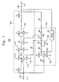
- the self-resetting inverter circuit 100 includes a logic input terminal 102 for receiving an input signal IN, an inverter logic circuit 104 for performing a logical inverting operation with respect to the input signal IN, a reset circuit 106 for resetting the inverter logic circuit 104, and a logic output terminal 108 for providing an output signal OUT.
- a PMOS transistor 10 of a smaller size than the normal transistor size and a typical dynamic inverter 114 consisting of one PMOS transistor 12 and two NMOS transistors 14 and 16
- the conduction path (i.e., source-drain channel) of the transistor 10 is coupled between a supply voltage terminal 110 and a node N1.
- the input signal IN is commonly applied to gates of the transistors 10 and 14 via the input terminal 102.
- PMOS transistor 12 has its conduction path coupled between the supply voltage terminal 110 and the node N1.
- the conduction paths ofNMOS transistors 14 and 15 are connected in series between the node N1 and a ground voltage terminal 112.
- Both a standard CMOS static inverter 116 (consisting of a PMOS transistor 18 and a smaller NMOS transistor 20) and another inverter 118 (consisting of a smaller PMOS transistor 24 and a larger NMOS transistor 26) are connected in series between the node N1 and the logic output terminal 108.
- a larger NMOS transistor 22 has its conduction path coupled between the ground voltage terminal 112 and the junction node N2 of the inverters 116 and 118.
- a larger PMOS transistor 28 is provided between the inverter 118 and the logic output terminal 108 and has its conduction path coupled between the supply voltage terminal 110 and the logic output terminal 108.
- a standard inverter 30 and a dynamic inverter 120 (consisting of one PMOS transistor 32 and two NMOS transistors 34 and 36) are provided for the reset circuit 106. Conduction paths of the transistors 32, 34 and 36 are connected in series between the supply voltage terminal 110 and the ground voltage terminal 112. The input signal IN is also fed via the inverter 30 to the gate of NMOS transistor 34.
- An inverting latch 122 consisting of cross-coupled standard inverters 38 and 40 is provided between the drain junction node N3 of transistors 32 and 34 and a node N4 coupled to gates of the transistors 12 and 16.
- two standard inverters 42 and 44 are provided for the reset circuit 106.
- the inverter 42 has its input coupled to the node N5 and its output coupled a node N6 which is coupled to the gate of NMOS transistor 22.
- the inverter 44 has its input coupled to the node N6 and its output coupled to the gate ofPMOS transistor 28 via a node N7. Further, the output signal OUT is fed back to the reset circuit 106, and provided through a delay circuit 46 to a node N3 commonly coupled to gates of the transistors 32 and 36.
- NMOS transistors 34 and 36 within reset circuit 106 become conductive, so that nodes N4 and N6 are pulled down to a logic low level (i.e., about ground voltage V SS ), and nodes N5 and N7 are pulled up to a logic high level (i.e., about supply voltage V DD ).
- NMOS transistor 16 within inverter logic circuit 104 thus becomes conductive so as to be ready for the next logical operation.
- node N1 When input signal IN is making a transition from a logic low level to a logic high level, node N1 is then discharged to a logic low level since NMOS transistors 14 and 16 both are conducting, thereby causing the output signal OUT to change from a logic high level to a logic low level.
- This high-to-low transition of the output signal OUT is fed back to node N3 via delay circuit 46, and thus node N4 goes high because PMOS transistor 32 conducts then.
- the logic high level on node N4 makes nodes N5 and N7 low and node N6 high. Owing to the logic low level at nodes N5 and N7 and the logic high level at node N6, the transistors 12, 22 and 28 are turned on, but the transistor 16 is turned off. Therefore, the inverter logic circuit 104 is reset by reset circuit 106. That is, the node N1 and the logic output terminal 108 are precharged high again. Like this, the logic circuit 100 itself enters reset state by use of its reset circuit 106.
- the low-to-high transition of the output signal OUT on the terminal 108 is also sent to node N3 via the delay circuit 46, so that PMOS transistor 32 are turned off and NMOS transistor 36 on.
- NMOS transistor 34 still remains in off state, with the help of latch 122, nodes N5, N6 and N7 remain in the same states (i.e., N5 and N7 are low and node N6 is high) while input signal IN is maintained at high level.
- node N4 goes low since NMOS transistors 34 and 36 both are rendered conductive, making nodes N5 and N7 high and node N6 low.
- NMOS transistor 16 is turned on and PMOS transistor 28 off so that inverter logic circuit 104 is ready for the next pulse input of signal IN.
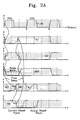
- Figs. 2A and 2B are timing diagrams exemplifying operational errors. As can be seen in Figs.
- the above-mentioned arrangement may be unsuitable for high speed and high performance applications because of its long feedback delay time (the output feedback through the delay circuit 40 occurs twice a cycle time). Further, ifdynamic logic circuits with the above circuit configuration are connected in series on a plurality of connected stages in semiconductor integrated circuits, since the respective stage output pulse widths are increased gradually with the advance ofthe stages, controlling the timing of the integrated circuit may be very difficult.
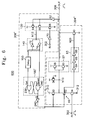
- the dynamic circuit 300 shown in Fig. 3 is a self-resetting dynamic inverter logic circuit, which includes an input terminal 302 for receiving an input signal IN, an inverter logic circuit 304 for inverting the input signal IN and providing an output signal OUT, a reset circuit 306 for resetting the inverter logic circuit 304, and an output terminal 308 for outputting the output signal OUT.
- the logic circuit 304 includes a dynamic inverter 49 consisting of a PMOS transistor 50, and NMOS transistors 52 and 54; and a PMOS transistor 56 of a smaller size than the normal transistor size.
- the transistors 50, 52 and 54 has their conduction paths (i.e., channels) coupled in series between a first supply voltage terminal 310 (i.e., a higher supply voltage terminal V DD ) and a second supply voltage terminal 312 (i.e., a lower supply voltage terminal such as a ground terminal V SS ) in order.
- Gates of the transistors 50 and 52 are coupled with each other.
- Transistor 54 has its gate applied with an input signal IN.
- Transistor 56 has its conduction path coupled between the first supply voltage terminal 310 and the drain junction node N10 of transistors 50 and 52 (i.e., output terminal 308), and its gate coupled to the second supply voltage terminal 312.
- the logic circuit 304 with the above arrangement functions as an inverter logic to perform the logic negation operation with respect to the input signal IN.
- the reset circuit 306 includes two static CMOS inverters 70 and 160; a dynamic inverter 130 consisting of a PMOS transistor 64 and NMOS transistors 66 and 68; an inverting latch 140 consisting of two cross-coupled static inverters 72 and 74; a delay circuit 150 formed by, for example, an even number of serially-connected static inverters (not shown); and an S(set)-R(reset) latch or flipflop 182 constructed from two NAND logic gates 80 and 82 connected back to back. Conduction paths of the transistors 64, 66 and 68 are coupled in series between the first and second supply voltage terminals 310 and 312 in order. Gates of the transistors 64 and 66 are commonly coupled to the output terminal 308.
- the input signal IN is supplied through inverter 70 to gate ofthe transistor 68.
- One terminal of the inverting latch 140 is coupled with drain junction node N12 of the transistors 64 and 66 and the other terminal thereof is commonly coupled with the delay circuit 150 and input terminal of the inverter 160.
- One input of NAND logic gate 80 i.e., Set input of flipflop 182 is coupled with delay circuit 150, and the other input thereof is coupled to output of NAND logic gate 82.
- NAND logic gate 82 has its one input coupled to output of NAND logic gate 80 and its other input coupled to output of inverter 160.
- Output ofNAND logic gate 82 i.e., negative output (generally represented by symbol Q ) of flipflop 182 is coupled with gates of transistors 50 and 52.
- NMOS transistor 54 When input signal IN is at a logic low level, then NMOS transistor 54 is turned off and node N10 is charged by PMOS transistor 56 to a logic high level, along with output terminal 308 (or output signal OUT). With high level output signal OUT, node N12 goes low since NMOS transistors 66 and 68 both are turned on, so nodes N14 and N16 go high and low, respectively. S-R flipflop 182 thus provides its output of a high level to node N18 (the output of the flipflop 182 will not change unless its inputs change). NMOS transistor 52 becomes conductive. Therefore, dynamic inverter logic circuit 300 is ready for the change of input signal IN.
- node N12 goes high.
- the logic high level on node N12 makes node N16 (i.e., the Reset input of S-R flipflop 182) high, output of the flipflop 182 with the high level Set input on node N14 then does not change and still remains high.
- a predetermined delay time e.g., 0.5 to 1.5 nsec
- the inverter logic circuit 304 is reset by reset circuit 306; that is, the dynamic inverter logic circuit 300 is reset by itself with the lapse of the delay time of delay circuit 150.
- the pulse width of the output signal OUT can be controlled by adjusting the delay time of the delay circuit 150 in a given operation cycle time.
- the low-to-high transition ofthe output signal OUT is also fed back to reset circuit 306, so that PMOS and NMOS transistors 64 and 68 are turned off and on, respectively.
- the dynamic inverter circuit 300 is ready for the low-to-high change of input signal IN.
- the input signal IN still remains high with the high level output signal OUT, although the transistor 68 is nonconductive, nodes N12 and N16 remain low and node N18 remains high with the help ofthe inverting latch 140, like the above case. Consequently, the dynamic inverter circuit 300 is also ready for the low-to-high change of input signal IN in this case. It will be well understood therefore that the dynamic logic circuit 300 enters a ready state independent of the pulse width of the input signal IN.
- the high-to-low transition of the output signal OUT is transferred to the Set input of flipflop 182 via delay circuit 150 to insure a desired output signal pulse width.
- the low-to-high transition of the output signal OUT is directly fed back to the Reset input of flipflop 182 without delay in order to prepare for next operation cycle quickly.
- Such a circuit configuration allows the dynamic circuit 300 to enter a reset state only depending on the low-to-high transition ofthe output signal OUT and independent of input pulse width although the delay time change due to process and/or environment variations occurs, thereby resulting in stable reset operation and preventing operational errors in high speed applications.
- Fig. 4 shows a second embodiment of a self-resetting dynamic logic circuit according to the invention.
- this embodied logic circuit 400 is a self-resetting dynamic buffer circuit, which has the same arrangement as that shown in Fig. 3 with exception that a static CMOS inverter 57, a delay circuit 83 and NMOS transistor 90 are additionally provided for buffer logic circuit 304', and a static inverter 62 for reset circuit 306'.
- the same parts as those shown in Fig. 3 are represented with like reference numerals and symbols and to avoid description duplication, accordingly, the explanation associated with their circuit configuration will be omitted.
- inverter 57 consisting of a larger PMOS transistor 58 and a smaller NMOS transistor 60 has its input coupled to node N10 and its output coupled to output terminal 308.
- Inverter 62 has its input coupled to output terminal 308 and its output coupled to the input of inverter 130.
- Delay circuit 83 constructed with three serially-connected static inverters 84, 86 and 88 is coupled between node N18 (or gate of transistor 52) and gate oftransistor 90 having its conduction path coupled between output terminal 308 and second supply voltage terminal (i.e., V SS ) 312.
- Fig. 5 the timing relationship between the signals at selected points ofthe logic circuit of Fig. 4 is shown.
- the operation ofthe self-resetting dynamic buffer logic circuit 400 will be described below with reference to Figs. 4 and 5.
- the low-to-high transition of the output signal OUT is transferred to reset circuit 306', and thus PMOS transistor 64 conducts while NMOS transistors 66 and 68 are rendered off, causing node N12 to go high.
- the logic high level on node N12 makes node N16 (i.e., the Reset input of S-R flipflop 182) high, output of the flipflop 182 with the high level Set input on node N14 then does not change and still remains high.
- a predetermined delay time e.g., 0.5 to 1.5 nsec
- delay circuit 150 After a predetermined delay time (e.g., 0.5 to 1.5 nsec) of delay circuit 150 has elapsed, nodes N14 and N18 go low. So, PMOS transistor 50 is turned on while NMOS transistor 52 is turned off, thus node N10 is recharged to a high level.
- the buffer logic circuit 304' is reset by reset circuit 306'.
- the self-resetting dynamic buffer logic circuit 400 is reset by itself with the lapse ofthe delay time of delay circuit 150.
- the pulse width of the output signal OUT can be controlled by adjusting the delay time of the delay circuit 150 in a given operation cycle time.
- the high-to-low transition ofthe output signal OUT is also fed back to reset circuit 306', so that PMOS and NMOS transistors 64 and 68 are turned off and on, respectively.
- the input signal IN has already gone low, then nodes N12 and N16 go low and node N18 goes high.
- PMOS and NMOS transistor 50 and 52 are switched off and on, respectively, so that the dynamic buffer circuit 300 is ready for the next low-to-high change of input signal IN.
- the dynamic buffer logic circuit 400 also enters a ready state independent of the pulse width of the input signal IN so as to be ready for the low-to-high change of input signal IN.
- the low-to-high transition the output signal OUT is transferred to the Set input of flipflop 182 via delay circuit 150 to insure a desired output signal pulse width.
- the high-to-low transition ofthe output signal OUT is directly fed back to the Reset input of flipflop 182 without delay in order to prepare for next operation cycle quickly.
- Such a circuit configuration allows the dynamic circuit 400 to enter a reset state only depending on the high-to-low transition of the output signal OUT and independent of input pulse width although the delay time change due to process and/or environment variations occurs, thereby resulting in stable reset operation and preventing operational errors in high speed applications (such as processors, or memories) in which logic circuits are cascaded in a plurality of connected stages.
- Fig. 6 illustrates a third embodiment of a self-resetting dynamic logic circuit according to the invention.
- this embodied logic circuit 600 is a self-resetting dynamic buffer circuit, which has the same arrangement as that shown in Fig. 4 with exception that inverter 160, S-R flipflop 182 and delay 150 are respectively replaced by a static inverter 242, an S-R flipflop 182' consisting of NOR logic gates 238 and 240, and an inverting delay circuit 150' consisting of, for example, an odd number of serially-connected inverters (not shown).
- the same parts as those shown in Fig. 4 are represented with like reference numerals and to avoid description duplication, accordingly, their explanation will be omitted.
- S-R flipflop 182' has a Set input coupled with delay circuit 150 and a Reset input coupled with latch 140.
- Input of inverter 242 is coupled to positive output (generally represented by Q) ofthe flipflop 182' (i.e., output of NOR gate 240) and output ofthe inverter 242 is coupled in common to gates oftransistors 50 and 52 and to delay circuit 82.
- FIG. 7 A fourth embodiment of a self-resetting dynamic logic circuit according to the invention is depicted in Fig. 7, wherein there is illustrated a self-resetting dynamic inverter logic circuit 700.
- This self-resetting logic circuit 700 includes an input terminal 702 for receiving an input signal IN, an inverter logic circuit 704 for inverting the input signal IN and providing an output signal OUT, a reset circuit 706 for resetting the inverter logic circuit 704, and an output terminal 708 for outputting the output signal OUT.
- the logic circuit 704 includes a dynamic inverter 201 consisting of PMOS transistors 200 and 202, and an NMOS transistor 204; and a smaller NMOS transistor 206.
- the transistors 200, 202 and 204 have their conduction paths coupled in series between a higher supply voltage terminal (V DD ) 710 and a lower supply voltage terminal 712 such as a ground terminal (V SS ) in order. Gates of the transistors 200 and 204 are coupled with each other.
- Transistor 202 has its gate applied with an input signal IN.
- NMOS transistor 206 has its conduction path coupled between the higher supply voltage terminal 710 and the drain junction node of transistors 202 and 204 (i.e., output terminal 708), and its gate coupled to the higher supply voltage terminal 710.
- the logic circuit 704 with the above arrangement functions as an inverter logic to performs the logic negation operation with respect to the input signal IN.
- the reset circuit 706 includes two static CMOS inverters 213 and 223; a dynamic inverter 215 consisting of PMOS transistors 216 and 218, and an NMOS transistor 220; an inverting latch 217 consisting of two cross-coupled static inverters 224 and 222; a delay circuit 219 formed by, for example, an odd number of serially-connected static inverters (not shown); and an S-R flipflop 221 constructed with two cross-coupled NAND logic gates 230 and 232. Conduction paths of the transistors 216, 218 and 220 are coupled in series between the higher and lower supply voltage terminals 710 and 712 in order. Gates of the transistors 216 and 220 are commonly coupled to the output terminal 708.
- the input signal IN is supplied through inverter 213 to gate of the transistor 218.
- One terminal of the inverting latch 217 is coupled with drain junction node N22 of the transistors 218 and 220 and the other terminal thereof is commonly coupled with the delay circuit 219 and a Reset input of flipflop 221.
- a Set input of flipflop 221 is coupled with delay circuit 219.
- Negative output ( Q ) of flipflop 221 i.e., output of NAND logic gate 232
- output terminal 708 is then charged to a logic high level because NMOS transistor 206 has a much smaller size than PMOS transistors 200 and 202.
- the low-to-high transition ofthe output signal OUT is fed back to reset circuit 706, and thus NMOS transistor 220 conducts while PMOS transistors 216 and 218 are turned off, so that node N22 goes low.
- the logic low level on node N22 makes the Reset input of S-R flipflop 221 high, output ( Q ) of flipflop 221 still having the high level Set input does not change and remains high.
- a predetermined delay time e.g., 0.5 to 1.5 nsec
- flipflop 221 This causes flipflop 221 to provide its output ofa low level, so PMOS transistor 200 and NMOS transistor are rendered off and on, respectively, thereby causing output terminal 708 to be pulled down to a low level.
- the inverter logic circuit 704 is reset by reset circuit 706. That is, the dynamic inverter logic circuit 700 is reset by itself with the lapse of the delay time of delay circuit 219. Note that the pulse width of the output signal OUT can be controlled by adjusting the delay time of the delay circuit 150 within a given operation cycle time.
- the high-to-low transition ofthe output signal OUT is also fed back to reset circuit 706, so that PMOS transistor 216 is turned on.
- node N22 and Set input of flipflop 221 go low and thus PMOS and NMOS transistors 200 and 204 are switched off and on, respectively. Therefore, the dynamic inverter circuit 700 is ready for the high-to-low change of input signal IN.
- Set and Reset inputs of flipflop 221 are held at their previous states (i.e., low and high levels, respectively) with the help of inverting latch 217.
- the flipflop 221 thus provides its negative output of a low level so that PMOS and NMOS transistors 200 and 204 are turned off and on respectively and the low state of the output signal OUT is maintained stable.
- the dynamic logic circuit 700 of this embodiment does not affected by the pulse width ofthe input signal IN.
- the low-to-high transition the output signal OUT is transferred to the Set input of flipflop 221 via delay circuit 219 to insure a desired output signal pulse width.
- the high-to-low transition of the output signal OUT is directly fed back to the Reset input of flipflop 221 without delay in order to prepare for next operation cycle quickly.
- This embodied logic circuit 800 is a self-resetting dynamic buffer circuit, which has the same arrangement as that shown in Fig. 7 with exception that static CMOS inverters 207 and 234, and PMOS transistor 236 are additionally provided for buffer logic circuit 704', and a static inverter 214 for reset circuit 706'.
- the same parts as those shown in Fig. 7 are represented with like reference numerals and symbols.
- the principal operation of this self-resetting dynamic buffer logic circuit 800 can be well understood well in the light of that of the circuit shown in Fig. 7 and, therefore, their explanation will be omitted herein.
- Fig. 9 shows a sixth embodiment of a self-resetting dynamic logic circuit according to the invention.
- the dynamic logic circuit 900 shown in Fig. 9 is a self-resetting dynamic NAND logic circuit.
- the self-resetting dynamic NAND logic circuit 900 includes input terminals 902a, 902b and 902c for receiving input signals IN1, IN2 and IN3, respectively; a NAND logic circuit 904 for performing the logical NAND operation with respect to the input signals IN1, IN2 and IN3, and providing an output signal OUT; a reset circuit 906 for resetting the NAND logic circuit 904; and an output terminal 908 for outputting the output signal OUT.
- the NAND logic circuit 904 is formed by PMOS transistors 2 and 3, and NMOS transistors 4, 5, 6 and 8. Conduction paths of transistors 2, 4, 5, 6 and 8 are coupled in series between a higher supply voltage terminal (V DD ) 910 and a lower supply voltage terminal (V SS ) 912 in order. Input signals IN1, IN2 and IN3 are applied to gates of NMOS transistors 4, 5 and 6, respectively.
- PMOS transistor 3 of a smaller size than normal transistor size has its conduction path coupled between the higher supply voltage terminal 910 and the output terminal 908 (or the drain junction nodes of transistors 2 and 4) and its gate coupled to the lower supply voltage terminal 912.
- the reset circuit 906 is constructed with an S-R flipflop 920 made up of two NAND logic gates 922 and 924 connected back to back, and a delay circuit 930 consisting of, for example, an even number of serially-connected inverters (not shown).
- S-R flipflop 920 has its Set input coupled with the output terminal 908 and its Reset input supplied with the input signal IN1.
- One end of delay circuit 930 is coupled with negative output ( Q ) of flipflop 920, and the other end thereof is commonly coupled with gates of transistors 2 and 8.
- Fig. 10 is a timing diagram illustrating the timing relationship between the signals at selected points ofthe circuit of Fig. 9. The operation ofthe self-resetting dynamic logic circuit 900 will be described with reference to Figs. 9 and 10.
- NMOS transistors 4, 5 and 6 are turned off and S-R flipflop 920 produces its negative output ( Q ) (i.e., reset signal rs0) of a high level.
- Delay circuit 930 having a predetermined delay time (about 1 nsec) delays the reset signal rs0 and produces a delayed reset signal rsl of a high level.
- PMOS transistor 2 and NMOS transistor 8 are turned off and on respectively in response to the delayed reset signal rs1, and thus output terminal 908 is charged by PMOS transistor 3 to a high level.
- Self-resetting dynamic NAND logic circuit 900 therefore, is ready for the change of input signals IN1, IN2 and IN3.
- output signal OUT on output terminal 908 goes low since all of NMOS transistors 4, 5, 6 and 8 which are larger than PMOS transistor 3 in size, become conductive.
- the low level on output terminal 908 makes negative output ( Q ) of flipflop 920 or reset signal rs0 low.
- the reset signal rs1 goes low and transistors 2 and 8 are switched on and off, respectively.
- This causes the output signal OUT to be recharged to a high level quickly even though the input signals IN 1, IN2 and IN3 are still remain high, as shown in Fig. 10. That is, NAND logic circuit 904 is reset by reset circuit 906 regardless of the pulse widths ofthe input signals IN1, IN2 and IN3.
- the pulse width of output signal OUT can be controlled by adjusting the delay time of delay circuit 930.
- NAND logic circuit 904 enters a ready state in which NMOS transistor 8 is conducting and ready for the change of input signals IN1, IN2 and IN3.
- the self-resetting dynamic NAND logic circuit 900 of Fig. 9 can be utilized for decoder circuits of memory devices.
- a circuit can function as a self-resetting dynamic inverter logic circuit with respect to a single input signal IN1.
Landscapes
- Engineering & Computer Science (AREA)
- Computer Hardware Design (AREA)
- Physics & Mathematics (AREA)
- Computing Systems (AREA)
- General Engineering & Computer Science (AREA)
- Mathematical Physics (AREA)
- Power Engineering (AREA)
- Microelectronics & Electronic Packaging (AREA)
- Logic Circuits (AREA)
- Pulse Circuits (AREA)
Applications Claiming Priority (2)
| Application Number | Priority Date | Filing Date | Title |
|---|---|---|---|
| KR1019970081005A KR100272672B1 (ko) | 1997-12-31 | 1997-12-31 | 다이나믹 씨모오스 회로 |
| KR9781005 | 1997-12-31 |
Publications (2)
| Publication Number | Publication Date |
|---|---|
| EP0928069A2 true EP0928069A2 (de) | 1999-07-07 |
| EP0928069A3 EP0928069A3 (de) | 2000-02-23 |
Family
ID=19530478
Family Applications (1)
| Application Number | Title | Priority Date | Filing Date |
|---|---|---|---|
| EP98309421A Withdrawn EP0928069A3 (de) | 1997-12-31 | 1998-11-18 | Selbstrücksetzende dynamische logische Schaltungen und Verfahren dazu |
Country Status (5)
| Country | Link |
|---|---|
| US (1) | US6275069B1 (de) |
| EP (1) | EP0928069A3 (de) |
| JP (1) | JP3841578B2 (de) |
| KR (1) | KR100272672B1 (de) |
| TW (1) | TW392107B (de) |
Families Citing this family (9)
| Publication number | Priority date | Publication date | Assignee | Title |
|---|---|---|---|---|
| US6496038B1 (en) * | 2000-06-30 | 2002-12-17 | Intel Corporation | Pulsed circuit topology including a pulsed, domino flip-flop |
| US6542006B1 (en) | 2000-06-30 | 2003-04-01 | Intel Corporation | Reset first latching mechanism for pulsed circuit topologies |
| US6567337B1 (en) | 2000-06-30 | 2003-05-20 | Intel Corporation | Pulsed circuit topology to perform a memory array write operation |
| US6531897B1 (en) | 2000-06-30 | 2003-03-11 | Intel Corporation | Global clock self-timed circuit with self-terminating precharge for high frequency applications |
| US6957371B2 (en) * | 2001-12-04 | 2005-10-18 | Intellitech Corporation | Method and apparatus for embedded built-in self-test (BIST) of electronic circuits and systems |
| JP5025172B2 (ja) * | 2005-09-28 | 2012-09-12 | エスケーハイニックス株式会社 | スルー−レートが制御されたオープン−ループ出力ドライバー |
| US7429884B2 (en) * | 2005-11-18 | 2008-09-30 | Sun Microsystems, Inc. | Pulse-signaling circuits for networks on chip |
| US7830176B2 (en) * | 2006-07-27 | 2010-11-09 | Arm Limited | Controlling signal levels on a signal line within an integrated circuit |
| US20090167395A1 (en) * | 2007-12-31 | 2009-07-02 | Texas Instruments Incorporated | High performance latches |
Family Cites Families (14)
| Publication number | Priority date | Publication date | Assignee | Title |
|---|---|---|---|---|
| IT1139929B (it) * | 1981-02-06 | 1986-09-24 | Rca Corp | Circuito generatore di impulsi utilizzante una sorgente di corrente |
| JPS59151523A (ja) * | 1983-02-14 | 1984-08-30 | Toshiba Corp | 遷移検出回路 |
| US4751407A (en) | 1986-12-19 | 1988-06-14 | Hughes Aircraft Company | Self-timing circuit |
| IT1244205B (it) * | 1990-12-19 | 1994-07-08 | Sgs Thomson Microelectronics | Circuito di generazione di un clock di scansione in un dispositivo di analisi operativa di tipo seriale per circuito integrato |
| JP3467286B2 (ja) * | 1992-05-19 | 2003-11-17 | ヒューレット・パッカード・カンパニー | 論理評価システム |
| US5374894A (en) * | 1992-08-19 | 1994-12-20 | Hyundai Electronics America | Transition detection circuit |
| US5291076A (en) * | 1992-08-31 | 1994-03-01 | Motorola, Inc. | Decoder/comparator and method of operation |
| US5430399A (en) * | 1993-04-19 | 1995-07-04 | Sun Microsystems, Inc. | Reset logic circuit and method |
| US5465060A (en) | 1994-06-10 | 1995-11-07 | International Business Machines Corporation | Fast edge triggered self-resetting CMOS receiver with parallel L1/L2 (Master/Slave) latch |
| US5488319A (en) * | 1994-08-18 | 1996-01-30 | International Business Machines Corporation | Latch interface for self-reset logic |
| US5467037A (en) * | 1994-11-21 | 1995-11-14 | International Business Machines Corporation | Reset generation circuit to reset self resetting CMOS circuits |
| US5550490A (en) | 1995-05-25 | 1996-08-27 | International Business Machines Corporation | Single-rail self-resetting logic circuitry |
| US5650733A (en) | 1995-10-24 | 1997-07-22 | International Business Machines Corporation | Dynamic CMOS circuits with noise immunity |
| US5986475A (en) * | 1997-06-26 | 1999-11-16 | Sun Microsystems, Inc. | Apparatus and method for resetting a dynamic logic circuit |
-
1997
- 1997-12-31 KR KR1019970081005A patent/KR100272672B1/ko not_active Expired - Fee Related
-
1998
- 1998-10-30 TW TW087118025A patent/TW392107B/zh not_active IP Right Cessation
- 1998-11-18 EP EP98309421A patent/EP0928069A3/de not_active Withdrawn
- 1998-12-28 JP JP37258998A patent/JP3841578B2/ja not_active Expired - Fee Related
- 1998-12-29 US US09/222,497 patent/US6275069B1/en not_active Expired - Lifetime
Also Published As
| Publication number | Publication date |
|---|---|
| TW392107B (en) | 2000-06-01 |
| KR19990060761A (ko) | 1999-07-26 |
| KR100272672B1 (ko) | 2000-11-15 |
| JP3841578B2 (ja) | 2006-11-01 |
| US6275069B1 (en) | 2001-08-14 |
| JPH11330948A (ja) | 1999-11-30 |
| EP0928069A3 (de) | 2000-02-23 |
Similar Documents
| Publication | Publication Date | Title |
|---|---|---|
| US6078201A (en) | Power-on reset circuit for dual supply voltages | |
| JP3272382B2 (ja) | セットアップ時間の短い低電力cmosバスレシーバ | |
| US5917355A (en) | Edge-triggered staticized dynamic flip-flop with conditional shut-off mechanism | |
| US5334888A (en) | Fast exclusive-or and exclusive-nor gates | |
| US5087835A (en) | Positive edge triggered synchronized pulse generator | |
| US6111447A (en) | Timing circuit that selectively triggers on a rising or falling input signal edge | |
| US3971960A (en) | Flip-flop false output rejection circuit | |
| US6762957B2 (en) | Low clock swing latch for dual-supply voltage design | |
| EP0477706B1 (de) | Schaltung zum Synchronisieren von asynchronen Zustandsmaschinen | |
| US6191618B1 (en) | Contention-free, low clock load domino circuit topology | |
| EP0928069A2 (de) | Selbstrücksetzende dynamische logische Schaltungen und Verfahren dazu | |
| US4314166A (en) | Fast level shift circuits | |
| KR0163447B1 (ko) | 데이터 아웃 버퍼회로 | |
| JP2004159111A (ja) | 高電圧検出回路 | |
| US6504412B1 (en) | Storage element with switched capacitor | |
| US6380781B1 (en) | Soft error rate tolerant latch | |
| US5818264A (en) | Dynamic circuit having improved noise immunity and method therefor | |
| US6483363B1 (en) | Storage element with stock node capacitive load | |
| US11271549B2 (en) | Semiconductor device for controlling voltage at an input node of a circuit during a low power mode | |
| US10566959B1 (en) | Sense amplifier flip-flop and method for fixing setup time violations in an integrated circuit | |
| US6407608B1 (en) | Clock input buffer with increased noise immunity | |
| US20050040856A1 (en) | Domino circuitry compatible static latch | |
| US6069498A (en) | Clock generator for CMOS circuits with dynamic registers | |
| US6542006B1 (en) | Reset first latching mechanism for pulsed circuit topologies | |
| JP3109986B2 (ja) | 信号遷移検出回路 |
Legal Events
| Date | Code | Title | Description |
|---|---|---|---|
| PUAI | Public reference made under article 153(3) epc to a published international application that has entered the european phase |
Free format text: ORIGINAL CODE: 0009012 |
|
| 17P | Request for examination filed |
Effective date: 19981210 |
|
| AK | Designated contracting states |
Kind code of ref document: A2 Designated state(s): DE FR GB |
|
| AX | Request for extension of the european patent |
Free format text: AL;LT;LV;MK;RO;SI |
|
| PUAL | Search report despatched |
Free format text: ORIGINAL CODE: 0009013 |
|
| AK | Designated contracting states |
Kind code of ref document: A3 Designated state(s): AT BE CH CY DE DK ES FI FR GB GR IE IT LI LU MC NL PT SE |
|
| AX | Request for extension of the european patent |
Free format text: AL;LT;LV;MK;RO;SI |
|
| RIC1 | Information provided on ipc code assigned before grant |
Free format text: 7H 03K 19/096 A, 7H 03K 19/0948 B, 7H 03K 19/017 B |
|
| AKX | Designation fees paid |
Free format text: DE FR GB |
|
| 17Q | First examination report despatched |
Effective date: 20041220 |
|
| 17Q | First examination report despatched |
Effective date: 20041220 |
|
| GRAP | Despatch of communication of intention to grant a patent |
Free format text: ORIGINAL CODE: EPIDOSNIGR1 |
|
| STAA | Information on the status of an ep patent application or granted ep patent |
Free format text: STATUS: THE APPLICATION IS DEEMED TO BE WITHDRAWN |
|
| 18D | Application deemed to be withdrawn |
Effective date: 20100720 |