EP0925383B1 - Verfahren zur beschichtung von substraten durch cvd mit einer siliziumhaltigen schutzschicht - Google Patents
Verfahren zur beschichtung von substraten durch cvd mit einer siliziumhaltigen schutzschicht Download PDFInfo
- Publication number
- EP0925383B1 EP0925383B1 EP97940144A EP97940144A EP0925383B1 EP 0925383 B1 EP0925383 B1 EP 0925383B1 EP 97940144 A EP97940144 A EP 97940144A EP 97940144 A EP97940144 A EP 97940144A EP 0925383 B1 EP0925383 B1 EP 0925383B1
- Authority
- EP
- European Patent Office
- Prior art keywords
- substrate
- process according
- coating
- vapour deposition
- chemical vapour
- Prior art date
- Legal status (The legal status is an assumption and is not a legal conclusion. Google has not performed a legal analysis and makes no representation as to the accuracy of the status listed.)
- Expired - Lifetime
Links
- 239000000758 substrate Substances 0.000 title claims description 45
- 238000000034 method Methods 0.000 title claims description 30
- 238000000576 coating method Methods 0.000 title claims description 27
- 239000011248 coating agent Substances 0.000 title claims description 24
- XUIMIQQOPSSXEZ-UHFFFAOYSA-N Silicon Chemical compound [Si] XUIMIQQOPSSXEZ-UHFFFAOYSA-N 0.000 title claims description 9
- 238000005229 chemical vapour deposition Methods 0.000 title claims 5
- 239000011241 protective layer Substances 0.000 title description 12
- 239000007858 starting material Substances 0.000 claims description 15
- IJGRMHOSHXDMSA-UHFFFAOYSA-N Atomic nitrogen Chemical compound N#N IJGRMHOSHXDMSA-UHFFFAOYSA-N 0.000 claims description 14
- OKTJSMMVPCPJKN-UHFFFAOYSA-N Carbon Chemical compound [C] OKTJSMMVPCPJKN-UHFFFAOYSA-N 0.000 claims description 13
- 229910052799 carbon Inorganic materials 0.000 claims description 13
- 229910052710 silicon Inorganic materials 0.000 claims description 12
- 229910052757 nitrogen Inorganic materials 0.000 claims description 11
- 229910052751 metal Inorganic materials 0.000 claims description 9
- 239000002184 metal Substances 0.000 claims description 9
- 239000010703 silicon Substances 0.000 claims description 8
- FYJMSTYQFWCBNF-UHFFFAOYSA-N N-[amino(dimethylamino)boranyl]-1,1,1-tris(dimethylaminosilyl)-N-methylmethanamine Chemical compound CN(C)[SiH2]C(N(C)B(N(C)C)N)([SiH2]N(C)C)[SiH2]N(C)C FYJMSTYQFWCBNF-UHFFFAOYSA-N 0.000 claims description 6
- 125000000217 alkyl group Chemical group 0.000 claims description 5
- UFHFLCQGNIYNRP-UHFFFAOYSA-N Hydrogen Chemical compound [H][H] UFHFLCQGNIYNRP-UHFFFAOYSA-N 0.000 claims description 4
- 125000004432 carbon atom Chemical group C* 0.000 claims description 4
- 238000004518 low pressure chemical vapour deposition Methods 0.000 claims description 4
- QVGXLLKOCUKJST-UHFFFAOYSA-N atomic oxygen Chemical compound [O] QVGXLLKOCUKJST-UHFFFAOYSA-N 0.000 claims description 3
- 239000001257 hydrogen Substances 0.000 claims description 3
- 229910052739 hydrogen Inorganic materials 0.000 claims description 3
- 239000001301 oxygen Substances 0.000 claims description 3
- 229910052760 oxygen Inorganic materials 0.000 claims description 3
- 238000010438 heat treatment Methods 0.000 claims description 2
- 230000001681 protective effect Effects 0.000 claims 1
- 239000010410 layer Substances 0.000 description 20
- 229910052796 boron Inorganic materials 0.000 description 6
- VYPSYNLAJGMNEJ-UHFFFAOYSA-N Silicium dioxide Chemical compound O=[Si]=O VYPSYNLAJGMNEJ-UHFFFAOYSA-N 0.000 description 5
- 230000003647 oxidation Effects 0.000 description 5
- 238000007254 oxidation reaction Methods 0.000 description 5
- 239000000919 ceramic Substances 0.000 description 3
- 239000007788 liquid Substances 0.000 description 3
- XKRFYHLGVUSROY-UHFFFAOYSA-N Argon Chemical compound [Ar] XKRFYHLGVUSROY-UHFFFAOYSA-N 0.000 description 2
- ZOXJGFHDIHLPTG-UHFFFAOYSA-N Boron Chemical compound [B] ZOXJGFHDIHLPTG-UHFFFAOYSA-N 0.000 description 2
- 229910004298 SiO 2 Inorganic materials 0.000 description 2
- 239000000853 adhesive Substances 0.000 description 2
- 230000001070 adhesive effect Effects 0.000 description 2
- 238000000151 deposition Methods 0.000 description 2
- 230000008021 deposition Effects 0.000 description 2
- 239000011261 inert gas Substances 0.000 description 2
- 239000000155 melt Substances 0.000 description 2
- 238000002156 mixing Methods 0.000 description 2
- 238000002230 thermal chemical vapour deposition Methods 0.000 description 2
- 229910000831 Steel Inorganic materials 0.000 description 1
- 238000003917 TEM image Methods 0.000 description 1
- 229910001069 Ti alloy Inorganic materials 0.000 description 1
- 238000004125 X-ray microanalysis Methods 0.000 description 1
- 239000000443 aerosol Substances 0.000 description 1
- 229910052786 argon Inorganic materials 0.000 description 1
- 230000015572 biosynthetic process Effects 0.000 description 1
- 239000002131 composite material Substances 0.000 description 1
- 150000001875 compounds Chemical class 0.000 description 1
- 238000010276 construction Methods 0.000 description 1
- 238000001816 cooling Methods 0.000 description 1
- 229910052906 cristobalite Inorganic materials 0.000 description 1
- 238000001493 electron microscopy Methods 0.000 description 1
- 239000007789 gas Substances 0.000 description 1
- 239000011521 glass Substances 0.000 description 1
- 229910002804 graphite Inorganic materials 0.000 description 1
- 239000010439 graphite Substances 0.000 description 1
- 238000011835 investigation Methods 0.000 description 1
- 238000005461 lubrication Methods 0.000 description 1
- 238000002844 melting Methods 0.000 description 1
- 230000008018 melting Effects 0.000 description 1
- WCYWZMWISLQXQU-UHFFFAOYSA-N methyl Chemical compound [CH3] WCYWZMWISLQXQU-UHFFFAOYSA-N 0.000 description 1
- QJGQUHMNIGDVPM-UHFFFAOYSA-N nitrogen group Chemical group [N] QJGQUHMNIGDVPM-UHFFFAOYSA-N 0.000 description 1
- 230000035515 penetration Effects 0.000 description 1
- 238000005268 plasma chemical vapour deposition Methods 0.000 description 1
- 239000010453 quartz Substances 0.000 description 1
- 150000004756 silanes Chemical class 0.000 description 1
- HBMJWWWQQXIZIP-UHFFFAOYSA-N silicon carbide Chemical compound [Si+]#[C-] HBMJWWWQQXIZIP-UHFFFAOYSA-N 0.000 description 1
- 229910010271 silicon carbide Inorganic materials 0.000 description 1
- 239000010959 steel Substances 0.000 description 1
- 239000000126 substance Substances 0.000 description 1
- 238000005382 thermal cycling Methods 0.000 description 1
Classifications
-
- C—CHEMISTRY; METALLURGY
- C23—COATING METALLIC MATERIAL; COATING MATERIAL WITH METALLIC MATERIAL; CHEMICAL SURFACE TREATMENT; DIFFUSION TREATMENT OF METALLIC MATERIAL; COATING BY VACUUM EVAPORATION, BY SPUTTERING, BY ION IMPLANTATION OR BY CHEMICAL VAPOUR DEPOSITION, IN GENERAL; INHIBITING CORROSION OF METALLIC MATERIAL OR INCRUSTATION IN GENERAL
- C23C—COATING METALLIC MATERIAL; COATING MATERIAL WITH METALLIC MATERIAL; SURFACE TREATMENT OF METALLIC MATERIAL BY DIFFUSION INTO THE SURFACE, BY CHEMICAL CONVERSION OR SUBSTITUTION; COATING BY VACUUM EVAPORATION, BY SPUTTERING, BY ION IMPLANTATION OR BY CHEMICAL VAPOUR DEPOSITION, IN GENERAL
- C23C16/00—Chemical coating by decomposition of gaseous compounds, without leaving reaction products of surface material in the coating, i.e. chemical vapour deposition [CVD] processes
- C23C16/22—Chemical coating by decomposition of gaseous compounds, without leaving reaction products of surface material in the coating, i.e. chemical vapour deposition [CVD] processes characterised by the deposition of inorganic material, other than metallic material
- C23C16/30—Deposition of compounds, mixtures or solid solutions, e.g. borides, carbides, nitrides
-
- Y—GENERAL TAGGING OF NEW TECHNOLOGICAL DEVELOPMENTS; GENERAL TAGGING OF CROSS-SECTIONAL TECHNOLOGIES SPANNING OVER SEVERAL SECTIONS OF THE IPC; TECHNICAL SUBJECTS COVERED BY FORMER USPC CROSS-REFERENCE ART COLLECTIONS [XRACs] AND DIGESTS
- Y02—TECHNOLOGIES OR APPLICATIONS FOR MITIGATION OR ADAPTATION AGAINST CLIMATE CHANGE
- Y02T—CLIMATE CHANGE MITIGATION TECHNOLOGIES RELATED TO TRANSPORTATION
- Y02T50/00—Aeronautics or air transport
- Y02T50/60—Efficient propulsion technologies, e.g. for aircraft
Definitions
- the invention relates to a method for coating substrates by chemical vapor coating (CVD) with a silicon-containing protective layer.
- CVD chemical vapor coating
- quartz glass SiO 2
- silanes At a temperature above about 1,100 ° C, the amorphous quartz glass layer changes into the crystalline state (cristobalite). This so-called quartz crack leads to cracks in the coating, which lead to rapid oxidation of the carbon component, in particular after cooling and renewed heating of the component, that is to say when subjected to changes in temperature.
- Crack formation can be caused by additional layers, for example silicon carbide layers be pushed back, however, bringing up such an episode different layers connected with a corresponding number of process steps and thus costly and time consuming.
- the object of the invention is to use substrates of different types in a simple manner to provide a firmly adhering protective layer that can withstand high temperature changes withstands.
- R 1 is preferably a methyl radical and R 2 is hydrogen.
- R 2 is hydrogen.
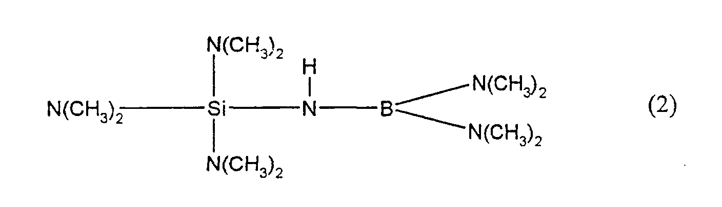
- tri (dimethylaminosilyl) amino-di (dimethylamino) borane is preferably used, which has the following structural formula (2):
- a thermal CVD process is preferably used as the CVD process, in particular an LPCVD (low pressure CVD) process.
- LPCVD low pressure CVD
- CVD processes can also use other CVD processes are used, in particular plasma CVD.
- the device for the thermal CVD method preferably has one pressure-tight reservoir on which the liquid starting compound according to the Contains formula (1) or (2) and by an inert gas, e.g. Argon, is under pressure.
- the liquid starting compound is a flow meter of a mixing device supplied, at the same time via a corresponding gas flow meter an inert gas, for example nitrogen, flows out, causing in the mixing device the liquid starting compound an aerosol is formed, which is heated in a Evaporator is evaporated without residue.
- the steam becomes one end preferably supplied tubular coating furnace, in which the coating substrate or a plurality of substrates one above the other and / or one behind the other are arranged. At the other end of the tubular furnace is a vacuum pump connected.
- the temperature of the evaporator is, for example, 40 ° C. to 150 ° C., preferably 75 ° C. to 100 ° C.
- the vacuum in the coating furnace can be 10 -1 to 10 -5 bar; normally it is 10 -2 to 10 -3 bar.
- the deposition conditions can adhered to precisely and therefore layers with very reproducible properties be preserved.
- the substrate is heated to a temperature of 400 ° C to 1800 ° C, especially 650 ° C to 1400 ° C heated. It can be used up to 1900 ° C Create an amorphous layer.
- the layer produced by the method according to the invention contains the elements (this term also includes bonds between them): silicon, nitrogen, Boron and carbon.
- the elements: Si, N and B can, as in the Starting compound, in a molar ratio of 1: 1: 1.
- the layer can contain organic residues resulting from the starting compound are formed, which influence the properties of the layer. If those organic residues are to be removed from the layer, the substrate is placed on a heated accordingly high temperature.
- the CVD deposition in the furnace can however, also take place at a rather lower temperature of the substrate and a thermal post-treatment carried out at 600 ° C to 1800 ° C in an oven to drive off the organic residues.
- the Si-N-B-C layer formed in this way is in particular for protecting metal parts suitable.
- the metal parts can be made of steel or a titanium alloy, for example consist.
- the protective layer applied to the metal part by the method according to the invention is characterized by a high adhesive strength. This then falls in particular extremely good if the metal part is coated in the unpolished state, i.e. one Has a roughness depth of more than 5 ⁇ m.
- the layer applied to the metal part by the method according to the invention exhibits high wear resistance and lubrication properties in addition to its high adhesive strength on.
- the latter can be determined by the proportion of organic residues derive from the alkyl groups of the starting substrate.
- the ceramic protective layer produced can, for example, the inventive method can be used to coat metal parts in engine construction.
- the method according to the invention is especially for coating carbon substrates or composite substrates made of carbon and silicon, which are highly suitable Are exposed to temperature, in particular high temperature changes, for example in space travel, e.g. for the nozzles of jet engines. It is also suitable for coating ceramic substrates.
- the Si on the surface of the protective layer is oxidized to SiO x , ie SiO and SiO 2 .
- This oxidation can be achieved by post-treatment of the coated substrate in one Oven, or when using the component in the air at high temperatures.
- the SiO x formed on the surface of the component has a relatively low melting point due to the boron.
- the protective layer melts in the surface area even at a relatively low temperature and the melt seals any cracks that may arise in the area below the protective layer, thereby preventing the penetration of oxygen to the carbon or carbon / silicon substrate.
- the SiO x content in the surface of the protective layer acts at high temperatures, while the Si-NBC phase of the remaining protective layer, that is to say the base layer, protects the component from oxidation at low temperatures.
- the nitrogenous substrates is to the nitrogenous substrates.
- a protective layer is produced by the method according to the invention previous processes the coated component even with thermal cycling reliably protects against oxidation up to 1900 ° C.
- Two substrates made of reaction-bonded Si 3 N 4 were heated to 900 ° C. in the coating furnace. 2 ml of the starting compound tri (dimethylaminosilyl) amino di (dimethylamino) borane were evaporated at 90 ° C. and passed through the coating oven. The pressure in the furnace was 5 x 10 -5 bar. After 90 minutes the starting compound was used up and the substrates were cooled to room temperature. One of the two substrates was coated again under the same conditions. The substrates were then aged in nitrogen at 1450 ° C. for 1 hour. The coatings evenly covered the substrates. X-ray electron microscopy (SEM) and transmission electron microscopy (TEM) images showed the intimate bond between the substrate and the first coating and between the first and second coatings. Both layers applied were amorphous. Electron dispersive X-ray (EDX) analyzes showed that the layer contained Si, N, B and C. The layer thickness was measured on the double-coated sample, it totaled 7 to 8 ⁇ m.
- Reaction-bonded Si 3 N 4 substrates were heated to 950 ° C. in the coating furnace.
- 4 ml of the starting compound tri (dimethylaminosilyl) amino-di (dimethylamino) borane were evaporated at 80 ° C. and passed into the coating oven.
- the pressure in the furnace was 2 x 10 -5 bar.
- the substrates were cooled to room temperature.
- the substrates were coated a second time under the same conditions.
- the substrates were then aged in nitrogen at 1450 ° C. for two hours. The coatings evenly covered the substrates.
- a graphite substrate was heated to 1000 ° C in the coating furnace. 1 ml of the starting compound tri (dimethylaminosilyl) amino di (dimethylamino) borane was evaporated at 100 ° C. and passed through the coating furnace. The pressure in the furnace was 2.7 x 10 -3 bar. After the starting compound had evaporated, the substrate was cooled to room temperature. The substrates were then aged in nitrogen at 1450 ° C. for one hour. The coating evenly covered the substrate. X-ray electron microscopic (SEM) investigations showed an intimate bond between the substrate and the coating. X-ray microanalysis showed Si, B, N and C in the layer. The layer thickness was 2.6 ⁇ m.
Landscapes
- Chemical & Material Sciences (AREA)
- Inorganic Chemistry (AREA)
- General Chemical & Material Sciences (AREA)
- Chemical Kinetics & Catalysis (AREA)
- Engineering & Computer Science (AREA)
- Materials Engineering (AREA)
- Mechanical Engineering (AREA)
- Metallurgy (AREA)
- Organic Chemistry (AREA)
- Chemical Vapour Deposition (AREA)
- Paints Or Removers (AREA)
Description

- R1
- eine Alkylgruppe mit 1 bis 4 Kohlenstoffatomen und
- R2
- Wasserstoff oder eine Alkylgruppe mit 1 bis 4 Kohlenstoffatomen ist.
Claims (9)
- Verfahren zur Beschichtung von Substraten durch chemische Dampfbeschichtung (CVD) mit einer siliziumhaltigen Schutzschicht, dadurch gekennzeichnet, daß zur chemischen Dampfbeschichtung eine Ausgangsverbindung folgender Strukturformel eingesetzt wird:worin

- R1
- eine Alkylgruppe mit 1 bis 4 Kohlenstoffatomen und
- R2
- Wasserstoff oder eine Alkylgruppe mit 1 bis 4 Kohlenstoffatomen ist.
- Verfahren nach Anspruch 1, dadurch gekennzeichnet, daß als Ausgangsverbindung Tri(dimethylaminosilyl)-amino-di(dimethylamino)boran eingesetzt wird.
- Verfahren nach Anspruch 1 oder 2, dadurch gekennzeichnet, daß die chemische Dampfbeschichtung durch thermische Dampfbeschichtung bei niedrigem Druck (LPCVD) erfolgt.
- Verfahren nach Anspruch 3, dadurch gekennzeichnet, daß der Druck 10-1 bis 10-5 bar beträgt.
- Verfahren nach einem der vorstehenden Ansprüche, dadurch gekennzeichnet, daß das Substrat während der Beschichtung auf eine Temperatur von 400°C bis 1800°C erwärmt wird.
- Verfahren nach einem der vorstehenden Ansprüche, dadurch gekennzeichnet, daß das Substrat nach der Beschichtung einer thermischen Nachbehandlung bei 600°C bis 1800°C unterworfen wird.
- Verfahren nach Anspruch 6, dadurch gekennzeichnet, daß das Substrat bei der Nachbehandlung einer sauerstoffhaltigen Atmosphäre ausgesetzt wird.
- Verfahren nach einem der vorstehenden Ansprüche, dadurch gekennzeichnet, das als Substrat ein Metall- oder ein Kohlenstoff-Substrat oder ein Substrat aus Kohlenstoff und Silizium oder ein Substrat aus Kohlenstoff, Stickstoff und Silizium oder Stickstoff und Silicium eingesetzt wird.
- Beschichtete Substrate, erhältlich nach einem Verfahren gemäß einem oder mehreren der vorangegangenen Ansprüche 1 bis 8.
Applications Claiming Priority (3)
| Application Number | Priority Date | Filing Date | Title |
|---|---|---|---|
| DE19635848 | 1996-09-04 | ||
| DE19635848A DE19635848C1 (de) | 1996-09-04 | 1996-09-04 | Verfahren zur Beschichtung von Substraten |
| PCT/EP1997/004715 WO1998010118A1 (de) | 1996-09-04 | 1997-08-29 | Verfahren zur beschichtung von substraten durch cvd mit einer siliziumhaltigen schutzschicht |
Publications (2)
| Publication Number | Publication Date |
|---|---|
| EP0925383A1 EP0925383A1 (de) | 1999-06-30 |
| EP0925383B1 true EP0925383B1 (de) | 2001-05-30 |
Family
ID=7804585
Family Applications (1)
| Application Number | Title | Priority Date | Filing Date |
|---|---|---|---|
| EP97940144A Expired - Lifetime EP0925383B1 (de) | 1996-09-04 | 1997-08-29 | Verfahren zur beschichtung von substraten durch cvd mit einer siliziumhaltigen schutzschicht |
Country Status (5)
| Country | Link |
|---|---|
| US (1) | US6177136B1 (de) |
| EP (1) | EP0925383B1 (de) |
| JP (1) | JP2001500926A (de) |
| DE (2) | DE19635848C1 (de) |
| WO (1) | WO1998010118A1 (de) |
Families Citing this family (2)
| Publication number | Priority date | Publication date | Assignee | Title |
|---|---|---|---|---|
| DE10045428A1 (de) | 2000-09-14 | 2002-03-28 | Max Planck Gesellschaft | Silicium-Bor-Kohlenstoff-Stickstoff-Keramiken und Vorläuferverbindungen, Verfahren zu deren Herstellung sowie deren Verwendung |
| US7297649B2 (en) | 2001-09-14 | 2007-11-20 | Max-Planck-Gesellschaft Zur Forderung Der Wissenschaften E.V. | Silicoboroncarbonitride ceramics and precursor compounds, method for the production and use thereof |
Family Cites Families (9)
| Publication number | Priority date | Publication date | Assignee | Title |
|---|---|---|---|---|
| GB792274A (en) * | 1955-11-08 | 1958-03-26 | Western Electric Co | Bodies having films of carbon, boron and silicon deposited thereon and methods of making such deposits |
| US4990365A (en) | 1988-08-17 | 1991-02-05 | Siemens Aktiengesellschaft | Method for producing silicon boronitride layers |
| DE4107108A1 (de) * | 1991-03-06 | 1992-09-10 | Bayer Ag | Siliciumbornitridkeramik und vorlaeuferverbindungen, verfahren zu deren herstellung sowie deren verwendung |
| DE4241288A1 (de) * | 1992-12-08 | 1994-06-09 | Bayer Ag | Polymere Borosilazane und Alumosilazane, Verfahren zu ihrer Herstellung sowie deren Verwendung |
| US5324690A (en) * | 1993-02-01 | 1994-06-28 | Motorola Inc. | Semiconductor device having a ternary boron nitride film and a method for forming the same |
| DE4425312A1 (de) * | 1994-07-18 | 1996-01-25 | Bayer Ag | Sinterwerkstoffe auf Basis von Si¶3¶N¶4¶/BN sowie Verfahren zu ihrer Herstellung |
| US5593728A (en) * | 1994-11-01 | 1997-01-14 | Advanced Ceramics Corporation | Interface coating for ceramic fibers |
| US5972511A (en) * | 1994-11-01 | 1999-10-26 | Advanced Ceramics Corporation | Process for forming low thermal expansion pyrolytic nitride coatings on low thermal expansion materials and coated article |
| US5952100A (en) * | 1997-05-21 | 1999-09-14 | General Electric Company | Silicon-doped boron nitride coated fibers in silicon melt infiltrated composites |
-
1996
- 1996-09-04 DE DE19635848A patent/DE19635848C1/de not_active Expired - Fee Related
-
1997
- 1997-08-29 WO PCT/EP1997/004715 patent/WO1998010118A1/de not_active Ceased
- 1997-08-29 EP EP97940144A patent/EP0925383B1/de not_active Expired - Lifetime
- 1997-08-29 US US09/242,975 patent/US6177136B1/en not_active Expired - Fee Related
- 1997-08-29 JP JP10512212A patent/JP2001500926A/ja active Pending
- 1997-08-29 DE DE59703686T patent/DE59703686D1/de not_active Expired - Fee Related
Also Published As
| Publication number | Publication date |
|---|---|
| US6177136B1 (en) | 2001-01-23 |
| EP0925383A1 (de) | 1999-06-30 |
| JP2001500926A (ja) | 2001-01-23 |
| WO1998010118A1 (de) | 1998-03-12 |
| DE59703686D1 (de) | 2001-07-05 |
| DE19635848C1 (de) | 1997-04-24 |
Similar Documents
| Publication | Publication Date | Title |
|---|---|---|
| DE60017823T2 (de) | Verfahren zum Aufbringen einer Barriereschicht auf ein siliziumhaltiges Substrat und nach diesem Verfahren hergestellter Gegenstand | |
| DE2020697C3 (de) | Verfahren zum Herstellen eines titanhaltigen Trägers mit einer Beschichtung | |
| DE69300369T2 (de) | Beschichteter Artikel. | |
| DE3243283C2 (de) | ||
| DE4112218A1 (de) | Ueberzugssysteme zum oxidationsschutz von titan | |
| US6645560B2 (en) | Oxidation resistant coatings for niobium-based silicide composites | |
| DE3719515A1 (de) | Oxidationsbeständiger Körper aus Kohlenstoff und Verfahren zu seiner Herstellung | |
| EP0200088B1 (de) | Verschleissfester beschichteter Hartmetallkörper und Verfahren zu seiner Herstellung | |
| EP0798402B1 (de) | Oxidationsschutzschicht | |
| EP3250724B1 (de) | Verfahren zum aufbringen eines metallischen schutzüberzugs auf eine oberfläche eines stahlprodukts | |
| DE2534777C2 (de) | Verfahren zum Verlöten eines polykristallinen Körpers aus hochhartem Werkstoff auf der Grundlage von Bornitrid und/oder Diamant mit einem Metallteil und Lot zur Durchführung dieses Verfahrens | |
| DE19635848C1 (de) | Verfahren zur Beschichtung von Substraten | |
| DE69503868T2 (de) | Verfahren und zusammensetzung zur verbindung von teilen aus keramik und feuerfester legierung | |
| DE69306302T2 (de) | Anwendung einer gegen Zinkschmelze beständige Legierung | |
| DE102004002303B4 (de) | Verfahren zur Herstellung eines beschichteten Kohlenstoff/Kohlenstoff-Verbundwerkstoffes und danach hergestellter beschichteter Kohlenstoff/Kohlenstoff-Verbundwerkstoff | |
| EP2855733B1 (de) | Verfahren zum beschichten eines kobalt-, nickel- und/oder eisenhaltigen substrats mit einer korrosionsbeständigen schicht | |
| DE10002876A1 (de) | Neue Aminosilylborylalkane, ihre Herstellung und Verwendung | |
| DE102006030235B4 (de) | Verfahren zum Schutz von Heißgaskorrosion von keramischen Oberflächen oder eines Körpers, hochtemperaturbeständiger Körper und deren Verwendung | |
| DE4034001C2 (de) | Schutzschicht gegen Hochtemperaturoxidation kohlenstoffenthaltender Bauteile sowie Verfahren zur Herstellung dieser Schicht | |
| DE69211423T2 (de) | Verfahren zur Herstellung einer metallischen Beschichtung auf einem Verbundkörper SiC/SiC | |
| DE2745812C2 (de) | Verfahren zum Auftragen einer siliziumhaltigen Schutzschicht | |
| US5389454A (en) | Silicide coating having good resistance to molten metals | |
| DE102004029070B4 (de) | Verfahren zum Eingießen eines Rohlings aus Eisenlegierung in ein Aluminium-Gussteil | |
| EP1496034B1 (de) | Hochtemperaturbeständiges Bauteil und Verfahren zu dessen Herstellung | |
| RU2855988C1 (ru) | Шликер для диффузной металлизации никелевых сплавов |
Legal Events
| Date | Code | Title | Description |
|---|---|---|---|
| PUAI | Public reference made under article 153(3) epc to a published international application that has entered the european phase |
Free format text: ORIGINAL CODE: 0009012 |
|
| 17P | Request for examination filed |
Effective date: 19990406 |
|
| AK | Designated contracting states |
Kind code of ref document: A1 Designated state(s): DE FR GB IT |
|
| GRAG | Despatch of communication of intention to grant |
Free format text: ORIGINAL CODE: EPIDOS AGRA |
|
| 17Q | First examination report despatched |
Effective date: 19990806 |
|
| GRAG | Despatch of communication of intention to grant |
Free format text: ORIGINAL CODE: EPIDOS AGRA |
|
| GRAG | Despatch of communication of intention to grant |
Free format text: ORIGINAL CODE: EPIDOS AGRA |
|
| GRAG | Despatch of communication of intention to grant |
Free format text: ORIGINAL CODE: EPIDOS AGRA |
|
| GRAH | Despatch of communication of intention to grant a patent |
Free format text: ORIGINAL CODE: EPIDOS IGRA |
|
| GRAH | Despatch of communication of intention to grant a patent |
Free format text: ORIGINAL CODE: EPIDOS IGRA |
|
| GRAA | (expected) grant |
Free format text: ORIGINAL CODE: 0009210 |
|
| AK | Designated contracting states |
Kind code of ref document: B1 Designated state(s): DE FR GB IT |
|
| REF | Corresponds to: |
Ref document number: 59703686 Country of ref document: DE Date of ref document: 20010705 |
|
| ITF | It: translation for a ep patent filed | ||
| GBT | Gb: translation of ep patent filed (gb section 77(6)(a)/1977) |
Effective date: 20010814 |
|
| ET | Fr: translation filed | ||
| REG | Reference to a national code |
Ref country code: GB Ref legal event code: IF02 |
|
| PLBE | No opposition filed within time limit |
Free format text: ORIGINAL CODE: 0009261 |
|
| STAA | Information on the status of an ep patent application or granted ep patent |
Free format text: STATUS: NO OPPOSITION FILED WITHIN TIME LIMIT |
|
| 26N | No opposition filed | ||
| PGFP | Annual fee paid to national office [announced via postgrant information from national office to epo] |
Ref country code: DE Payment date: 20030718 Year of fee payment: 7 |
|
| PGFP | Annual fee paid to national office [announced via postgrant information from national office to epo] |
Ref country code: FR Payment date: 20030805 Year of fee payment: 7 |
|
| PGFP | Annual fee paid to national office [announced via postgrant information from national office to epo] |
Ref country code: GB Payment date: 20030827 Year of fee payment: 7 |
|
| PG25 | Lapsed in a contracting state [announced via postgrant information from national office to epo] |
Ref country code: GB Free format text: LAPSE BECAUSE OF NON-PAYMENT OF DUE FEES Effective date: 20040829 |
|
| PG25 | Lapsed in a contracting state [announced via postgrant information from national office to epo] |
Ref country code: DE Free format text: LAPSE BECAUSE OF NON-PAYMENT OF DUE FEES Effective date: 20050301 |
|
| GBPC | Gb: european patent ceased through non-payment of renewal fee |
Effective date: 20040829 |
|
| PG25 | Lapsed in a contracting state [announced via postgrant information from national office to epo] |
Ref country code: FR Free format text: LAPSE BECAUSE OF NON-PAYMENT OF DUE FEES Effective date: 20050429 |
|
| REG | Reference to a national code |
Ref country code: FR Ref legal event code: ST |
|
| PG25 | Lapsed in a contracting state [announced via postgrant information from national office to epo] |
Ref country code: IT Free format text: LAPSE BECAUSE OF NON-PAYMENT OF DUE FEES Effective date: 20050829 |