EP0924820B1 - Polarisation-controlled VCSELS using externally applied unitaxial stress - Google Patents
Polarisation-controlled VCSELS using externally applied unitaxial stress Download PDFInfo
- Publication number
- EP0924820B1 EP0924820B1 EP98118381A EP98118381A EP0924820B1 EP 0924820 B1 EP0924820 B1 EP 0924820B1 EP 98118381 A EP98118381 A EP 98118381A EP 98118381 A EP98118381 A EP 98118381A EP 0924820 B1 EP0924820 B1 EP 0924820B1
- Authority
- EP
- European Patent Office
- Prior art keywords
- vcsel
- region
- axis
- mounting substrate
- substrate
- Prior art date
- Legal status (The legal status is an assumption and is not a legal conclusion. Google has not performed a legal analysis and makes no representation as to the accuracy of the status listed.)
- Expired - Lifetime
Links
- 239000000758 substrate Substances 0.000 claims description 64
- 230000010287 polarization Effects 0.000 claims description 41
- 239000010410 layer Substances 0.000 claims description 19
- 229910000679 solder Inorganic materials 0.000 claims description 16
- 238000000034 method Methods 0.000 claims description 12
- 230000001939 inductive effect Effects 0.000 claims description 11
- 239000012790 adhesive layer Substances 0.000 claims description 9
- 239000000463 material Substances 0.000 claims description 8
- 238000005530 etching Methods 0.000 claims description 2
- 239000004593 Epoxy Substances 0.000 description 5
- 239000004065 semiconductor Substances 0.000 description 5
- 230000003287 optical effect Effects 0.000 description 4
- 229910000980 Aluminium gallium arsenide Inorganic materials 0.000 description 2
- 229910001218 Gallium arsenide Inorganic materials 0.000 description 2
- 238000010276 construction Methods 0.000 description 2
- PCHJSUWPFVWCPO-UHFFFAOYSA-N gold Chemical compound [Au] PCHJSUWPFVWCPO-UHFFFAOYSA-N 0.000 description 2
- 239000010931 gold Substances 0.000 description 2
- 229910052737 gold Inorganic materials 0.000 description 2
- 229910000530 Gallium indium arsenide Inorganic materials 0.000 description 1
- BQCADISMDOOEFD-UHFFFAOYSA-N Silver Chemical compound [Ag] BQCADISMDOOEFD-UHFFFAOYSA-N 0.000 description 1
- 239000007767 bonding agent Substances 0.000 description 1
- 239000004020 conductor Substances 0.000 description 1
- 238000001816 cooling Methods 0.000 description 1
- 239000013078 crystal Substances 0.000 description 1
- 230000001627 detrimental effect Effects 0.000 description 1
- JVPLOXQKFGYFMN-UHFFFAOYSA-N gold tin Chemical compound [Sn].[Au] JVPLOXQKFGYFMN-UHFFFAOYSA-N 0.000 description 1
- 229910052739 hydrogen Inorganic materials 0.000 description 1
- 239000001257 hydrogen Substances 0.000 description 1
- -1 hydrogen ions Chemical class 0.000 description 1
- 238000004519 manufacturing process Methods 0.000 description 1
- 239000000203 mixture Substances 0.000 description 1
- 238000012986 modification Methods 0.000 description 1
- 230000004048 modification Effects 0.000 description 1
- 238000004806 packaging method and process Methods 0.000 description 1
- 238000007747 plating Methods 0.000 description 1
- 238000003825 pressing Methods 0.000 description 1
- 230000006798 recombination Effects 0.000 description 1
- 238000005215 recombination Methods 0.000 description 1
- 238000002310 reflectometry Methods 0.000 description 1
- 230000035945 sensitivity Effects 0.000 description 1
- 229910052709 silver Inorganic materials 0.000 description 1
- 239000004332 silver Substances 0.000 description 1
- 125000006850 spacer group Chemical group 0.000 description 1
- 230000002269 spontaneous effect Effects 0.000 description 1
Images

Classifications
-
- H—ELECTRICITY
- H01—ELECTRIC ELEMENTS
- H01S—DEVICES USING THE PROCESS OF LIGHT AMPLIFICATION BY STIMULATED EMISSION OF RADIATION [LASER] TO AMPLIFY OR GENERATE LIGHT; DEVICES USING STIMULATED EMISSION OF ELECTROMAGNETIC RADIATION IN WAVE RANGES OTHER THAN OPTICAL
- H01S5/00—Semiconductor lasers
- H01S5/10—Construction or shape of the optical resonator, e.g. extended or external cavity, coupled cavities, bent-guide, varying width, thickness or composition of the active region
- H01S5/18—Surface-emitting [SE] lasers, e.g. having both horizontal and vertical cavities
- H01S5/183—Surface-emitting [SE] lasers, e.g. having both horizontal and vertical cavities having only vertical cavities, e.g. vertical cavity surface-emitting lasers [VCSEL]
- H01S5/18355—Surface-emitting [SE] lasers, e.g. having both horizontal and vertical cavities having only vertical cavities, e.g. vertical cavity surface-emitting lasers [VCSEL] having a defined polarisation
-
- H—ELECTRICITY
- H01—ELECTRIC ELEMENTS
- H01S—DEVICES USING THE PROCESS OF LIGHT AMPLIFICATION BY STIMULATED EMISSION OF RADIATION [LASER] TO AMPLIFY OR GENERATE LIGHT; DEVICES USING STIMULATED EMISSION OF ELECTROMAGNETIC RADIATION IN WAVE RANGES OTHER THAN OPTICAL
- H01S5/00—Semiconductor lasers
- H01S5/02—Structural details or components not essential to laser action
- H01S5/022—Mountings; Housings
- H01S5/0235—Method for mounting laser chips
- H01S5/02355—Fixing laser chips on mounts
- H01S5/0237—Fixing laser chips on mounts by soldering
-
- H—ELECTRICITY
- H01—ELECTRIC ELEMENTS
- H01S—DEVICES USING THE PROCESS OF LIGHT AMPLIFICATION BY STIMULATED EMISSION OF RADIATION [LASER] TO AMPLIFY OR GENERATE LIGHT; DEVICES USING STIMULATED EMISSION OF ELECTROMAGNETIC RADIATION IN WAVE RANGES OTHER THAN OPTICAL
- H01S5/00—Semiconductor lasers
- H01S5/06—Arrangements for controlling the laser output parameters, e.g. by operating on the active medium
- H01S5/0607—Arrangements for controlling the laser output parameters, e.g. by operating on the active medium by varying physical parameters other than the potential of the electrodes, e.g. by an electric or magnetic field, mechanical deformation, pressure, light, temperature
Definitions
- the present invention relates to lasers, and more particularly, to an improved method for controlling the polarization of surface emitting laser diodes in an array of such diodes.
- VCSELs Vertical Cavity Surface-Emitting Lasers
- the optics which deliver the laser power to the disc or drum have a certain degree of polarization sensitivity, such that if the polarization of the light source drifts, the drift will translate into detrimental output power variations.
- the optics can be complex enough in these systems that knowledge of the polarization direction is necessary to optimize the optics design. For these reasons, the light sources for such applications must have a stable fixed polarization, and the polarization direction must be the same for every laser fabricated.
- the output light is, in general, a mixture of polarization states with ratio of the light in the fixed polarization state to the other polarization state typically of the order of 10:1.
- the polarization state is not always stable. For example, the polarization direction can often flip by 90° as current is increased beyond threshold and as the laser switches between modes.
- the polarization tends to be randomly oriented from device to device. This is due to the circular symmetry of typical VCSEL designs.
- Various methods have been applied to lock the polarization direction by adding some asymmetry to the cavity such as elliptical current confinement, or elliptical optical confinement, or both.
- these solutions have met with limited success in that the percentage of finished devices that remain locked in the desired polarization direction is significantly less than 100%.
- the beam shape is altered by some of the methods from the desirable circular output beam into a less desirable elliptical shape.
- US-A-5,394,423 discloses a VCSEL assembly which comprises a top mirror, a bottom mirror, a light generation region between said top and bottom mirror region, a conducting substrate, a bottom electrode and a strain inducing means for inducing a strain in said light generation region along two directions, i.e. an X axis and an Y axis.
- the present invention provides a VCSEL assembly according to claims 1, 2, and 6, respectively as well as a method for fabricating a VCSEL assembly according to claims 7 and 8, respectively.
- the present invention as defined in claims 1, 2, 6, 7 and 8, is a Vertical Cavity Surface-Emitting Laser (VCSEL) assembly in which the polarization is locked to a specified direction that is the same for all VCSELs.
- a VCSEL according to the present invention includes a VCSEL having a top mirror region, a bottom mirror region, a light generation region between the top and bottom mirror regions, a conducting substrate and a bottom electrode. The bottom mirror region is sandwiched between the conducting substrate and the light generation region, and the conducting substrate is sandwiched between the bottom electrode and the bottom mirror region.
- the assembly also includes a mounting substrate having top and bottom surfaces, the VCSEL being mechanically coupled to the mounting substrate.
- the mounting substrate includes a means for defining a first axis.
- the assembly includes a means for causing the mounting substrate to flex about the first axis thereby inducing a strain in the light generation region which locks the polarization into a mode determined by the first axis.
- the first axis is defined by a channel in the mounting substrate.
- the mounting substrate is caused to flex by the application of an adhesive layer applied between the mounting substrate and a mounting surface.
- the adhesive layer has a thermal coefficient of expansion different from the mounting substrate.
- the adhesive layer includes a solder layer that fills the channel. Upon cooling, the solder layer contracts causing the mounting substrate to flex.
- trenches whose direction defines the first axis are located in the top mirror region of the VCSEL.
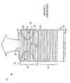
- FIG. 1 is a cross-sectional view of a conventional VCSEL 10. Since construction of VCSELs is well known to those skilled in the laser arts, it will not be described in detail here. For the purposes of this discussion, it is sufficient to note that VCSEL 10 may be viewed as a p-i-n diode having a top mirror region 18, a light generation region 14, and bottom mirror region 19. These regions are constructed on a substrate 12. Electrical power is applied between electrodes 22 and 27. The various layers are constructed by epitaxial growth.
- Substrate 12 is an n-type semiconductor in the example shown in Figure 1.
- the active region is typically constructed from one or more quantum wells of InGaAs, GaAs, AlGaAs, (Al)GaInP, GaInAsP or InAlGaAs which is separated from mirror regions 18 and 19 by spacers 15 and 16, respectively.
- the choice of material depends on the desired wavelength of the light emitted by the VCSEL and other desired VCSEL properties.
- devices based on bulk active regions are known to the art.
- This layer 14 may be viewed as a light generation layer which generates light due to spontaneous and stimulated emission via the recombination of electrons and holes generated by forward biasing the p-i-n diode.
- the mirror regions are constructed from alternating layers of which layers 20 and 21 are typical. These layers have different indices of refraction. The thickness of each layer is chosen to be one quarter of the wavelength of the light.
- the stacks form Bragg mirrors.
- the stacks are typically constructed from alternating layers of AlAs and GaAs or AlGaAs. To obtain the desired reflectivity, 20 to 30 pairs of layers are typically required.
- the layers in the upper mirror region 18 are typically doped to be p-type semiconductors and those in the lower mirror region 19 are doped to be n-type semiconductors.
- Substrate 12 is preferably n-type.
- Bottom electrode 27 is preferably an n-ohmic contact.
- n-i-p diode structures may also be constructed by growing the structures on a p-substrate or a semi-insulating substrate with a p-layer deposited thereon.
- the current flow between electrodes 22 and 27 is confined to region 24 by implanting regions 25 and 26 to convert the regions to regions of high resistivity. This is typically accomplished by implanting with hydrogen ions.
- VCSEL 10 is not shown to scale in Figure 1.
- the mirror regions and active regions have been expanded to provide clarity in the drawing.
- the thickness of region 12 is typically 150 ⁇ m compared to about 10 ⁇ m for the mirror and active regions.
- Window 30 in top electrode 22 is approximately 10 ⁇ m in diameter while bottom electrode 27 covers the bottom of the substrate.
- the present invention is based on the observation that uniaxial compressive stress enhances the optical gain for polarizations aligned along the stress axis.
- compressive stress applied along a [100] direction enhances the optical gain for polarizations along the stress axis by as much as ⁇ 1 cm -1 /[N/mm 2 ] relative to the optical gain for orthogonally polarized directions.
- the stress is externally introduced with a predetermined direction and magnitude sufficient to completely lock the polarization direction along the stress axis. It has been found experimentally that pressing down on a long thin semiconductor chip with a VCSEL on top applies enough compressive stress to the surface of the chip to lock the polarization of the VCSEL to the stress axis. It is estimated that the applied [110] directed stress required to lock the polarization is on the order of 10-100 N/mm 2 , and the corresponding strain in the crystal is on the order of 0.01-0.05%.
- This level of stress can be introduced by means of bonding the chip to a surface with a material which shrinks more than the VCSEL chip after the bonding process. Examples include solder, conductive epoxy, gold plating, and even dielectric films.
- a material which shrinks more than the VCSEL chip after the bonding process examples include solder, conductive epoxy, gold plating, and even dielectric films.
- the bowing of the chip must be constrained to one axis. In the preferred embodiment of the present invention, this is accomplished by removing a portion of the wafer on which the chip is constructed.
- FIG 2 is a perspective view of a chip 50 having a VCSEL 51 constructed on a wafer 52 in which the bottom side of wafer 52 has been partially cut away to form a slot 53 having an axis along which the stress is to be induced.
- the depth of slot 53 is typically 75 ⁇ m and the chip thickness is typically 150 ⁇ m in the preferred embodiment of the present invention.
- the slot is preferably created by etching channels on the backside of the wafer before cleaving the wafer into chips. The slot renders the chip more flexible in one direction. When the bonding agent shrinks, the chip is forced to bend in a direction determined by the slot axis.
- FIG. 3 is a cross-sectional view of a chip 112 having a VCSEL 111 mounted on a header 113 by a solder joint 114.
- the solder joint When the solder joint is applied, the solder is molten at a temperature of typically 275°C. As the solder cools and solidifies, the solder joint shrinks thus applying force to the chip in the direction shown by arrow 115.
- the solder also provides the electrical contact between header 113 and the bottom electrode of VCSEL 111.
- a gold-tin solder is preferred.
- the resulting stress pattern results in a maximum perpendicular-to-channel stress which is significantly more than the required 10-100 N/mm 2 stress required to provide polarization locking. It has been found experimentally that polarization ratios of greater than 100:1 may be obtained utilizing the preferred embodiment of the present invention described above.
- the VCSEL may be mounted on the header by a conductive epoxy joint.
- a conductive epoxy joint For example, a silver epoxy may be used.
- the device is baked at a temperature of typically 120°C for about 30 minutes to cure the epoxy joint.
- the epoxy joint shrinks as it cures, which applies a force to the chip in a manner similar to that described above.
- electrode 27 and substrate 12 shown in Figure 1 are incorporated into chip 112.
- Chip 112 is preferably constructed from an n-type semiconductor so that it is conductive. Chip 112 replaces substrate 12 shown in Figure 1.
- a metallic layer 117 is then applied to the bottom surface of chip 112 after the channel is etched in the bottom layer. This metallic layer serves the function of electrode 27.
- the VCSEL may be constructed as shown in Figure 1 with electrode 27 on the top surface of chip 112.
- the connection to electrode 27 may be made by metallic conductors on the surface of chip 112 and chip 112 can then be constructed from a non-conducting substrate.
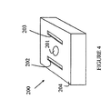
- FIG 4 is a perspective view of a chip 200 having a VCSEL 201 constructed thereon.
- Two trenches shown at 202 and 203 are etched on either side of VCSEL 201.
- the orientation of the trenches defines the orientation of the stress pattern applied to VCSEL 201.
- the trenches may be filled with a material that has a coefficient of thermal expansion that is different from that of the substrate.
- the trenches may be filled with solder, gold, or dielectric.
- the fill material is applied at a temperature well above the operating temperature of VCSEL 201. As the fill material cools a force is applied to the light generation region of the VCSEL. The direction of the force will depend on whether the fill material has a coefficient of thermal expansion that is greater than or less than that of the substrate.
- Embodiments in which the trenches are not filled have also been found to operate successfully to provide polarization locking.
- trenches having a width of 1-10 ⁇ m, a length of approximately twice the width of the VCSEL, and a depth of approximately the thickness of the top mirror region have been found to provide polarization locking. Deeper trenches also provide the desired polarization locking.
- the trenches may be etched from 1-10 ⁇ m from the VCSEL.
- the above described embodiments have assumed that the VCSEL has not been constructed in a manner in which one direction of polarization is favored.
- the present invention may also be used in conjunction with systems which provide imperfect polarization locking to provide a VCSEL with a very high degree of polarization locking.
- VCSELs with partial polarization locking by constructing the VCSEL on a mis-oriented substrate. While the polarization observed with such VCSELs tends to be determined by the substrate orientation, this method is not sufficiently reliable to assure that all of the VCSELs have the same direction of polarization after all of the fabrication and packaging operations have been completed.
- the combination of mis-oriented substrate construction and trenches along the VCSEL provides reliable polarization locking.
Landscapes
- Physics & Mathematics (AREA)
- Condensed Matter Physics & Semiconductors (AREA)
- General Physics & Mathematics (AREA)
- Electromagnetism (AREA)
- Optics & Photonics (AREA)
- Semiconductor Lasers (AREA)
Applications Claiming Priority (2)
| Application Number | Priority Date | Filing Date | Title |
|---|---|---|---|
| US08/993,006 US6188711B1 (en) | 1997-12-18 | 1997-12-18 | Polarization-controlled VCSELs using externally applied uniaxial stress |
| US993006 | 1997-12-18 |
Publications (3)
| Publication Number | Publication Date |
|---|---|
| EP0924820A2 EP0924820A2 (en) | 1999-06-23 |
| EP0924820A3 EP0924820A3 (en) | 1999-07-14 |
| EP0924820B1 true EP0924820B1 (en) | 2002-05-29 |
Family
ID=25538997
Family Applications (1)
| Application Number | Title | Priority Date | Filing Date |
|---|---|---|---|
| EP98118381A Expired - Lifetime EP0924820B1 (en) | 1997-12-18 | 1998-09-29 | Polarisation-controlled VCSELS using externally applied unitaxial stress |
Country Status (4)
| Country | Link |
|---|---|
| US (1) | US6188711B1 (OSRAM) |
| EP (1) | EP0924820B1 (OSRAM) |
| JP (1) | JP4359354B2 (OSRAM) |
| DE (1) | DE69805597T2 (OSRAM) |
Families Citing this family (18)
| Publication number | Priority date | Publication date | Assignee | Title |
|---|---|---|---|---|
| US6304588B1 (en) * | 1997-02-07 | 2001-10-16 | Xerox Corporation | Method and structure for eliminating polarization instability in laterally-oxidized VCSELs |
| JP3482824B2 (ja) * | 1997-07-29 | 2004-01-06 | セイコーエプソン株式会社 | 面発光型半導体レーザおよび面発光型半導体レーザアレイ |
| US7004644B1 (en) * | 1999-06-29 | 2006-02-28 | Finisar Corporation | Hermetic chip-scale package for photonic devices |
| EP1104056A1 (en) * | 1999-11-18 | 2001-05-30 | Avalon Photonics Ltd | A polarization controlled vertical-cavity surface-emitting laser |
| JP3944677B2 (ja) * | 1999-11-30 | 2007-07-11 | セイコーエプソン株式会社 | 面発光型半導体レーザの製造方法 |
| IL145245A0 (en) | 2001-09-03 | 2002-06-30 | Jtc 2000 Dev Delaware Inc | System and method including vector-matrix multiplication |
| US6785317B2 (en) * | 2001-09-10 | 2004-08-31 | Vrije Universiteit Brussels | Enhanced polarization control and stabilization by macroscopic in-plane anisotropic strain in vertical-cavity surface-emitting lasers |
| GB2379797A (en) * | 2001-09-15 | 2003-03-19 | Zarlink Semiconductor Ab | Surface Emitting Laser |
| DE10253908B4 (de) * | 2002-09-24 | 2010-04-22 | Osram Opto Semiconductors Gmbh | Strahlungsemittierendes Halbleiterbauelement |
| US7372886B2 (en) * | 2004-06-07 | 2008-05-13 | Avago Technologies Fiber Ip Pte Ltd | High thermal conductivity vertical cavity surface emitting laser (VCSEL) |
| JP4687064B2 (ja) * | 2004-10-22 | 2011-05-25 | ソニー株式会社 | 面発光型半導体レーザ素子 |
| JP5376104B2 (ja) * | 2005-07-04 | 2013-12-25 | ソニー株式会社 | 面発光型半導体レーザ |
| WO2013123241A1 (en) | 2012-02-17 | 2013-08-22 | The Regents Of The University Of California | Method for the reuse of gallium nitride epitaxial substrates |
| WO2014015337A2 (en) * | 2012-07-20 | 2014-01-23 | The Regents Of The University Of California | Structure and method for the fabrication of a gallium nitride vertical cavity surface emitting laser |
| DE102012021169B4 (de) * | 2012-10-29 | 2015-02-12 | Dausinger & Giesen Gmbh | Laserverstärkersystem mit angeklebter Festkörperscheibe |
| JP6786961B2 (ja) * | 2016-08-29 | 2020-11-18 | セイコーエプソン株式会社 | 面発光レーザーおよび原子発振器 |
| DK3791451T3 (da) * | 2018-05-11 | 2025-03-03 | Excelitas Tech Corp | Polarisationsstyring af afstembar vcsel ved hjælp af ikke-ensartede chipbindinger |
| DE102021212985A1 (de) * | 2021-11-18 | 2023-05-25 | Robert Bosch Gesellschaft mit beschränkter Haftung | Verfahren zur Herstellung einer Kamera und Kamera |
Citations (2)
| Publication number | Priority date | Publication date | Assignee | Title |
|---|---|---|---|---|
| WO1998053537A1 (en) * | 1997-05-17 | 1998-11-26 | University Of Bristol | Laser devices |
| EP0935321A1 (en) * | 1997-07-29 | 1999-08-11 | Seiko Epson Corporation | Surface emission semiconductor laser |
Family Cites Families (14)
| Publication number | Priority date | Publication date | Assignee | Title |
|---|---|---|---|---|
| US4474422A (en) | 1979-11-13 | 1984-10-02 | Canon Kabushiki Kaisha | Optical scanning apparatus having an array of light sources |
| WO1992021069A1 (fr) | 1991-05-14 | 1992-11-26 | Seiko Epson Corporation | Dispositif de formation d'image |
| JP2875929B2 (ja) | 1992-10-09 | 1999-03-31 | シャープ株式会社 | 半導体レーザ素子およびその製造方法 |
| JPH0773139B2 (ja) | 1993-01-26 | 1995-08-02 | 日本電気株式会社 | 面発光半導体レーザ |
| US5331654A (en) | 1993-03-05 | 1994-07-19 | Photonics Research Incorporated | Polarized surface-emitting laser |
| US5416044A (en) | 1993-03-12 | 1995-05-16 | Matsushita Electric Industrial Co., Ltd. | Method for producing a surface-emitting laser |
| US5345462A (en) | 1993-03-29 | 1994-09-06 | At&T Bell Laboratories | Semiconductor surface emitting laser having enhanced polarization control and transverse mode selectivity |
| JP3477744B2 (ja) | 1993-06-23 | 2003-12-10 | ソニー株式会社 | 発光装置及びこれを用いた立体視覚装置及びその視覚方法及びその駆動方法 |
| US5412680A (en) | 1994-03-18 | 1995-05-02 | Photonics Research Incorporated | Linear polarization of semiconductor laser |
| US5892784A (en) | 1994-10-27 | 1999-04-06 | Hewlett-Packard Company | N-drive p-common surface emitting laser fabricated on n+ substrate |
| US5493577A (en) | 1994-12-21 | 1996-02-20 | Sandia Corporation | Efficient semiconductor light-emitting device and method |
| JPH0964462A (ja) | 1995-08-24 | 1997-03-07 | Nec Corp | 面発光レーザ装置およびその製造方法 |
| US6002705A (en) * | 1997-12-03 | 1999-12-14 | Xerox Corporation | Wavelength and polarization multiplexed vertical cavity surface emitting lasers |
| US5953362A (en) * | 1997-12-15 | 1999-09-14 | Pamulapati; Jagadeesh | Strain induce control of polarization states in vertical cavity surface emitting lasers and method of making same |
-
1997
- 1997-12-18 US US08/993,006 patent/US6188711B1/en not_active Expired - Lifetime
-
1998
- 1998-09-29 EP EP98118381A patent/EP0924820B1/en not_active Expired - Lifetime
- 1998-09-29 DE DE69805597T patent/DE69805597T2/de not_active Expired - Lifetime
- 1998-12-04 JP JP34573498A patent/JP4359354B2/ja not_active Expired - Fee Related
Patent Citations (2)
| Publication number | Priority date | Publication date | Assignee | Title |
|---|---|---|---|---|
| WO1998053537A1 (en) * | 1997-05-17 | 1998-11-26 | University Of Bristol | Laser devices |
| EP0935321A1 (en) * | 1997-07-29 | 1999-08-11 | Seiko Epson Corporation | Surface emission semiconductor laser |
Also Published As
| Publication number | Publication date |
|---|---|
| EP0924820A3 (en) | 1999-07-14 |
| DE69805597T2 (de) | 2003-01-16 |
| EP0924820A2 (en) | 1999-06-23 |
| JP4359354B2 (ja) | 2009-11-04 |
| JPH11233899A (ja) | 1999-08-27 |
| US6188711B1 (en) | 2001-02-13 |
| DE69805597D1 (de) | 2002-07-04 |
Similar Documents
| Publication | Publication Date | Title |
|---|---|---|
| US6188711B1 (en) | Polarization-controlled VCSELs using externally applied uniaxial stress | |
| US6277696B1 (en) | Surface emitting laser using two wafer bonded mirrors | |
| US5416044A (en) | Method for producing a surface-emitting laser | |
| JP4174322B2 (ja) | 垂直共振器面発光レーザとその製造方法 | |
| US5953362A (en) | Strain induce control of polarization states in vertical cavity surface emitting lasers and method of making same | |
| US6222866B1 (en) | Surface emitting semiconductor laser, its producing method and surface emitting semiconductor laser array | |
| US6653158B2 (en) | Double intracavity contacted long-wavelength VCSELs and method of fabricating same | |
| US6542531B2 (en) | Vertical cavity surface emitting laser and a method of fabrication thereof | |
| Chang‐Hasnain et al. | Low threshold buried heterostructure vertical cavity surface emitting laser | |
| US5394423A (en) | Surface emitting semiconductor laser | |
| US5253263A (en) | High-power surface-emitting semiconductor injection laser with etched internal 45 degree and 90 degree micromirrors | |
| US4675875A (en) | Surface emitting semiconductor laser | |
| US7668219B2 (en) | Surface emitting semiconductor device | |
| EP1173908A2 (en) | Wavelength division multiplexed array of long-wavelength vertical cavity lasers | |
| JP2857256B2 (ja) | 垂直型半導体レーザ | |
| JP2000196189A (ja) | 面発光型半導体レーザ | |
| JPH11112081A (ja) | 半導体レーザ,及びその製造方法 | |
| EP0874425B1 (en) | Ring cavity type surface emitting semiconductor laser | |
| Ohnishi et al. | Continuous wave operation of surface emitting two-dimensional photonic crystal laser | |
| Iga | Surface emitting lasers | |
| CA2284319A1 (en) | Long wavelength vertical cavity laser with integrated short wavelength pump laser | |
| Bornholdt et al. | Passive optical GaInAsP/InP waveguides | |
| Wu et al. | High-yield processing and single-mode operation of passive antiguide region vertical-cavity lasers | |
| US6793388B2 (en) | Semiconductor laser and fabricating method of the same | |
| JP2875929B2 (ja) | 半導体レーザ素子およびその製造方法 |
Legal Events
| Date | Code | Title | Description |
|---|---|---|---|
| PUAI | Public reference made under article 153(3) epc to a published international application that has entered the european phase |
Free format text: ORIGINAL CODE: 0009012 |
|
| PUAL | Search report despatched |
Free format text: ORIGINAL CODE: 0009013 |
|
| AK | Designated contracting states |
Kind code of ref document: A2 Designated state(s): DE FR GB |
|
| AX | Request for extension of the european patent |
Free format text: AL;LT;LV;MK;RO;SI |
|
| AK | Designated contracting states |
Kind code of ref document: A3 Designated state(s): AT BE CH CY DE DK ES FI FR GB GR IE IT LI LU MC NL PT SE |
|
| AX | Request for extension of the european patent |
Free format text: AL;LT;LV;MK;RO;SI |
|
| 17P | Request for examination filed |
Effective date: 19991210 |
|
| AKX | Designation fees paid |
Free format text: DE FR GB |
|
| 17Q | First examination report despatched |
Effective date: 20000602 |
|
| RAP1 | Party data changed (applicant data changed or rights of an application transferred) |
Owner name: AGILENT TECHNOLOGIES, INC. |
|
| RIC1 | Information provided on ipc code assigned before grant |
Free format text: 7H 01S 5/183 A, 7H 01S 5/022 B, 7H 01L 33/00 B |
|
| RAP1 | Party data changed (applicant data changed or rights of an application transferred) |
Owner name: AGILENT TECHNOLOGIES INC. |
|
| GRAG | Despatch of communication of intention to grant |
Free format text: ORIGINAL CODE: EPIDOS AGRA |
|
| RAP1 | Party data changed (applicant data changed or rights of an application transferred) |
Owner name: AGILENT TECHNOLOGIES INC. A DELAWARE CORPORATION |
|
| RIC1 | Information provided on ipc code assigned before grant |
Free format text: 7H 01S 5/183 A, 7H 01S 5/022 B, 7H 01L 33/00 B |
|
| RAP1 | Party data changed (applicant data changed or rights of an application transferred) |
Owner name: AGILENT TECHNOLOGIES, INC. (A DELAWARE CORPORATION |
|
| GRAG | Despatch of communication of intention to grant |
Free format text: ORIGINAL CODE: EPIDOS AGRA |
|
| GRAH | Despatch of communication of intention to grant a patent |
Free format text: ORIGINAL CODE: EPIDOS IGRA |
|
| GRAH | Despatch of communication of intention to grant a patent |
Free format text: ORIGINAL CODE: EPIDOS IGRA |
|
| GRAA | (expected) grant |
Free format text: ORIGINAL CODE: 0009210 |
|
| AK | Designated contracting states |
Kind code of ref document: B1 Designated state(s): DE FR GB |
|
| PG25 | Lapsed in a contracting state [announced via postgrant information from national office to epo] |
Ref country code: FR Free format text: LAPSE BECAUSE OF FAILURE TO SUBMIT A TRANSLATION OF THE DESCRIPTION OR TO PAY THE FEE WITHIN THE PRESCRIBED TIME-LIMIT Effective date: 20020529 |
|
| REG | Reference to a national code |
Ref country code: GB Ref legal event code: FG4D |
|
| REF | Corresponds to: |
Ref document number: 69805597 Country of ref document: DE Date of ref document: 20020704 |
|
| PGFP | Annual fee paid to national office [announced via postgrant information from national office to epo] |
Ref country code: FR Payment date: 20020830 Year of fee payment: 5 |
|
| EN | Fr: translation not filed | ||
| PLBE | No opposition filed within time limit |
Free format text: ORIGINAL CODE: 0009261 |
|
| STAA | Information on the status of an ep patent application or granted ep patent |
Free format text: STATUS: NO OPPOSITION FILED WITHIN TIME LIMIT |
|
| 26N | No opposition filed |
Effective date: 20030303 |
|
| REG | Reference to a national code |
Ref country code: GB Ref legal event code: 732E |
|
| REG | Reference to a national code |
Ref country code: GB Ref legal event code: 732E Free format text: REGISTERED BETWEEN 20130725 AND 20130731 |
|
| PGFP | Annual fee paid to national office [announced via postgrant information from national office to epo] |
Ref country code: GB Payment date: 20150825 Year of fee payment: 18 Ref country code: DE Payment date: 20150820 Year of fee payment: 18 |
|
| REG | Reference to a national code |
Ref country code: DE Ref legal event code: R119 Ref document number: 69805597 Country of ref document: DE |
|
| GBPC | Gb: european patent ceased through non-payment of renewal fee |
Effective date: 20160929 |
|
| PG25 | Lapsed in a contracting state [announced via postgrant information from national office to epo] |
Ref country code: DE Free format text: LAPSE BECAUSE OF NON-PAYMENT OF DUE FEES Effective date: 20170401 Ref country code: GB Free format text: LAPSE BECAUSE OF NON-PAYMENT OF DUE FEES Effective date: 20160929 |