EP0918353A1 - A method of manufacturing a recessed insulated gate field-effect semiconductor device - Google Patents
A method of manufacturing a recessed insulated gate field-effect semiconductor device Download PDFInfo
- Publication number
- EP0918353A1 EP0918353A1 EP99200133A EP99200133A EP0918353A1 EP 0918353 A1 EP0918353 A1 EP 0918353A1 EP 99200133 A EP99200133 A EP 99200133A EP 99200133 A EP99200133 A EP 99200133A EP 0918353 A1 EP0918353 A1 EP 0918353A1
- Authority
- EP
- European Patent Office
- Prior art keywords
- region
- layer
- gate
- define
- conductivity type
- Prior art date
- Legal status (The legal status is an assumption and is not a legal conclusion. Google has not performed a legal analysis and makes no representation as to the accuracy of the status listed.)
- Withdrawn
Links
- 239000004065 semiconductor Substances 0.000 title claims abstract description 55
- 230000005669 field effect Effects 0.000 title claims abstract description 21
- 238000004519 manufacturing process Methods 0.000 title claims abstract description 9
- 238000005530 etching Methods 0.000 claims abstract description 17
- 239000002019 doping agent Substances 0.000 claims abstract description 12
- 239000012212 insulator Substances 0.000 claims abstract description 12
- 239000004020 conductor Substances 0.000 claims abstract description 10
- 238000000034 method Methods 0.000 claims description 35
- 230000003064 anti-oxidating effect Effects 0.000 claims description 12
- 229910021420 polycrystalline silicon Inorganic materials 0.000 claims description 9
- IJGRMHOSHXDMSA-UHFFFAOYSA-N Atomic nitrogen Chemical compound N#N IJGRMHOSHXDMSA-UHFFFAOYSA-N 0.000 claims description 6
- MWUXSHHQAYIFBG-UHFFFAOYSA-N Nitric oxide Chemical compound O=[N] MWUXSHHQAYIFBG-UHFFFAOYSA-N 0.000 claims description 6
- 229910052757 nitrogen Inorganic materials 0.000 claims description 3
- 239000002800 charge carrier Substances 0.000 claims description 2
- 239000011521 glass Substances 0.000 claims description 2
- 230000000717 retained effect Effects 0.000 claims 1
- 230000003647 oxidation Effects 0.000 description 21
- 238000007254 oxidation reaction Methods 0.000 description 21
- 125000006850 spacer group Chemical group 0.000 description 15
- 239000012535 impurity Substances 0.000 description 6
- 239000000463 material Substances 0.000 description 6
- 239000000758 substrate Substances 0.000 description 6
- 241000293849 Cordylanthus Species 0.000 description 5
- XUIMIQQOPSSXEZ-UHFFFAOYSA-N Silicon Chemical compound [Si] XUIMIQQOPSSXEZ-UHFFFAOYSA-N 0.000 description 5
- 238000001465 metallisation Methods 0.000 description 5
- 230000008569 process Effects 0.000 description 5
- 229910052710 silicon Inorganic materials 0.000 description 5
- 239000010703 silicon Substances 0.000 description 5
- 230000001681 protective effect Effects 0.000 description 4
- 238000011109 contamination Methods 0.000 description 3
- 238000009792 diffusion process Methods 0.000 description 3
- 239000011810 insulating material Substances 0.000 description 3
- QGZKDVFQNNGYKY-UHFFFAOYSA-N Ammonia Chemical compound N QGZKDVFQNNGYKY-UHFFFAOYSA-N 0.000 description 2
- 229910052581 Si3N4 Inorganic materials 0.000 description 2
- VYPSYNLAJGMNEJ-UHFFFAOYSA-N Silicium dioxide Chemical compound O=[Si]=O VYPSYNLAJGMNEJ-UHFFFAOYSA-N 0.000 description 2
- 230000009471 action Effects 0.000 description 2
- 230000008901 benefit Effects 0.000 description 2
- 238000000151 deposition Methods 0.000 description 2
- 238000012986 modification Methods 0.000 description 2
- 230000004048 modification Effects 0.000 description 2
- 230000003071 parasitic effect Effects 0.000 description 2
- HQVNEWCFYHHQES-UHFFFAOYSA-N silicon nitride Chemical compound N12[Si]34N5[Si]62N3[Si]51N64 HQVNEWCFYHHQES-UHFFFAOYSA-N 0.000 description 2
- 229910052814 silicon oxide Inorganic materials 0.000 description 2
- 238000009825 accumulation Methods 0.000 description 1
- XAGFODPZIPBFFR-UHFFFAOYSA-N aluminium Chemical compound [Al] XAGFODPZIPBFFR-UHFFFAOYSA-N 0.000 description 1
- 229910052782 aluminium Inorganic materials 0.000 description 1
- 229910021529 ammonia Inorganic materials 0.000 description 1
- 210000003323 beak Anatomy 0.000 description 1
- 230000015572 biosynthetic process Effects 0.000 description 1
- 238000004140 cleaning Methods 0.000 description 1
- 230000003749 cleanliness Effects 0.000 description 1
- 238000007796 conventional method Methods 0.000 description 1
- 238000005516 engineering process Methods 0.000 description 1
- 230000002708 enhancing effect Effects 0.000 description 1
- 238000010438 heat treatment Methods 0.000 description 1
- 238000002513 implantation Methods 0.000 description 1
- 230000006698 induction Effects 0.000 description 1
- 230000000873 masking effect Effects 0.000 description 1
- 229910021421 monocrystalline silicon Inorganic materials 0.000 description 1
- 238000012856 packing Methods 0.000 description 1
- 230000009467 reduction Effects 0.000 description 1
- 239000012925 reference material Substances 0.000 description 1
Images


Classifications
-
- H—ELECTRICITY
- H01—ELECTRIC ELEMENTS
- H01L—SEMICONDUCTOR DEVICES NOT COVERED BY CLASS H10
- H01L29/00—Semiconductor devices adapted for rectifying, amplifying, oscillating or switching, or capacitors or resistors with at least one potential-jump barrier or surface barrier, e.g. PN junction depletion layer or carrier concentration layer; Details of semiconductor bodies or of electrodes thereof ; Multistep manufacturing processes therefor
- H01L29/66—Types of semiconductor device ; Multistep manufacturing processes therefor
- H01L29/68—Types of semiconductor device ; Multistep manufacturing processes therefor controllable by only the electric current supplied, or only the electric potential applied, to an electrode which does not carry the current to be rectified, amplified or switched
- H01L29/76—Unipolar devices, e.g. field effect transistors
- H01L29/772—Field effect transistors
- H01L29/78—Field effect transistors with field effect produced by an insulated gate
- H01L29/7801—DMOS transistors, i.e. MISFETs with a channel accommodating body or base region adjoining a drain drift region
- H01L29/7802—Vertical DMOS transistors, i.e. VDMOS transistors
- H01L29/7813—Vertical DMOS transistors, i.e. VDMOS transistors with trench gate electrode, e.g. UMOS transistors
-
- H—ELECTRICITY
- H01—ELECTRIC ELEMENTS
- H01L—SEMICONDUCTOR DEVICES NOT COVERED BY CLASS H10
- H01L29/00—Semiconductor devices adapted for rectifying, amplifying, oscillating or switching, or capacitors or resistors with at least one potential-jump barrier or surface barrier, e.g. PN junction depletion layer or carrier concentration layer; Details of semiconductor bodies or of electrodes thereof ; Multistep manufacturing processes therefor
- H01L29/66—Types of semiconductor device ; Multistep manufacturing processes therefor
- H01L29/66007—Multistep manufacturing processes
- H01L29/66075—Multistep manufacturing processes of devices having semiconductor bodies comprising group 14 or group 13/15 materials
- H01L29/66227—Multistep manufacturing processes of devices having semiconductor bodies comprising group 14 or group 13/15 materials the devices being controllable only by the electric current supplied or the electric potential applied, to an electrode which does not carry the current to be rectified, amplified or switched, e.g. three-terminal devices
- H01L29/66234—Bipolar junction transistors [BJT]
- H01L29/66325—Bipolar junction transistors [BJT] controlled by field-effect, e.g. insulated gate bipolar transistors [IGBT]
- H01L29/66333—Vertical insulated gate bipolar transistors
- H01L29/66348—Vertical insulated gate bipolar transistors with a recessed gate
-
- H—ELECTRICITY
- H01—ELECTRIC ELEMENTS
- H01L—SEMICONDUCTOR DEVICES NOT COVERED BY CLASS H10
- H01L29/00—Semiconductor devices adapted for rectifying, amplifying, oscillating or switching, or capacitors or resistors with at least one potential-jump barrier or surface barrier, e.g. PN junction depletion layer or carrier concentration layer; Details of semiconductor bodies or of electrodes thereof ; Multistep manufacturing processes therefor
- H01L29/66—Types of semiconductor device ; Multistep manufacturing processes therefor
- H01L29/66007—Multistep manufacturing processes
- H01L29/66075—Multistep manufacturing processes of devices having semiconductor bodies comprising group 14 or group 13/15 materials
- H01L29/66227—Multistep manufacturing processes of devices having semiconductor bodies comprising group 14 or group 13/15 materials the devices being controllable only by the electric current supplied or the electric potential applied, to an electrode which does not carry the current to be rectified, amplified or switched, e.g. three-terminal devices
- H01L29/66409—Unipolar field-effect transistors
- H01L29/66477—Unipolar field-effect transistors with an insulated gate, i.e. MISFET
- H01L29/66674—DMOS transistors, i.e. MISFETs with a channel accommodating body or base region adjoining a drain drift region
- H01L29/66712—Vertical DMOS transistors, i.e. VDMOS transistors
- H01L29/66719—With a step of forming an insulating sidewall spacer
-
- H—ELECTRICITY
- H01—ELECTRIC ELEMENTS
- H01L—SEMICONDUCTOR DEVICES NOT COVERED BY CLASS H10
- H01L29/00—Semiconductor devices adapted for rectifying, amplifying, oscillating or switching, or capacitors or resistors with at least one potential-jump barrier or surface barrier, e.g. PN junction depletion layer or carrier concentration layer; Details of semiconductor bodies or of electrodes thereof ; Multistep manufacturing processes therefor
- H01L29/66—Types of semiconductor device ; Multistep manufacturing processes therefor
- H01L29/66007—Multistep manufacturing processes
- H01L29/66075—Multistep manufacturing processes of devices having semiconductor bodies comprising group 14 or group 13/15 materials
- H01L29/66227—Multistep manufacturing processes of devices having semiconductor bodies comprising group 14 or group 13/15 materials the devices being controllable only by the electric current supplied or the electric potential applied, to an electrode which does not carry the current to be rectified, amplified or switched, e.g. three-terminal devices
- H01L29/66409—Unipolar field-effect transistors
- H01L29/66477—Unipolar field-effect transistors with an insulated gate, i.e. MISFET
- H01L29/66674—DMOS transistors, i.e. MISFETs with a channel accommodating body or base region adjoining a drain drift region
- H01L29/66712—Vertical DMOS transistors, i.e. VDMOS transistors
- H01L29/66727—Vertical DMOS transistors, i.e. VDMOS transistors with a step of recessing the source electrode
-
- H—ELECTRICITY
- H01—ELECTRIC ELEMENTS
- H01L—SEMICONDUCTOR DEVICES NOT COVERED BY CLASS H10
- H01L29/00—Semiconductor devices adapted for rectifying, amplifying, oscillating or switching, or capacitors or resistors with at least one potential-jump barrier or surface barrier, e.g. PN junction depletion layer or carrier concentration layer; Details of semiconductor bodies or of electrodes thereof ; Multistep manufacturing processes therefor
- H01L29/66—Types of semiconductor device ; Multistep manufacturing processes therefor
- H01L29/68—Types of semiconductor device ; Multistep manufacturing processes therefor controllable by only the electric current supplied, or only the electric potential applied, to an electrode which does not carry the current to be rectified, amplified or switched
- H01L29/70—Bipolar devices
- H01L29/72—Transistor-type devices, i.e. able to continuously respond to applied control signals
- H01L29/739—Transistor-type devices, i.e. able to continuously respond to applied control signals controlled by field-effect, e.g. bipolar static induction transistors [BSIT]
- H01L29/7393—Insulated gate bipolar mode transistors, i.e. IGBT; IGT; COMFET
- H01L29/7395—Vertical transistors, e.g. vertical IGBT
- H01L29/7396—Vertical transistors, e.g. vertical IGBT with a non planar surface, e.g. with a non planar gate or with a trench or recess or pillar in the surface of the emitter, base or collector region for improving current density or short circuiting the emitter and base regions
- H01L29/7397—Vertical transistors, e.g. vertical IGBT with a non planar surface, e.g. with a non planar gate or with a trench or recess or pillar in the surface of the emitter, base or collector region for improving current density or short circuiting the emitter and base regions and a gate structure lying on a slanted or vertical surface or formed in a groove, e.g. trench gate IGBT
-
- H—ELECTRICITY
- H01—ELECTRIC ELEMENTS
- H01L—SEMICONDUCTOR DEVICES NOT COVERED BY CLASS H10
- H01L21/00—Processes or apparatus adapted for the manufacture or treatment of semiconductor or solid state devices or of parts thereof
- H01L21/02—Manufacture or treatment of semiconductor devices or of parts thereof
- H01L21/04—Manufacture or treatment of semiconductor devices or of parts thereof the devices having at least one potential-jump barrier or surface barrier, e.g. PN junction, depletion layer or carrier concentration layer
- H01L21/18—Manufacture or treatment of semiconductor devices or of parts thereof the devices having at least one potential-jump barrier or surface barrier, e.g. PN junction, depletion layer or carrier concentration layer the devices having semiconductor bodies comprising elements of Group IV of the Periodic System or AIIIBV compounds with or without impurities, e.g. doping materials
- H01L21/22—Diffusion of impurity materials, e.g. doping materials, electrode materials, into or out of a semiconductor body, or between semiconductor regions; Interactions between two or more impurities; Redistribution of impurities
- H01L21/225—Diffusion of impurity materials, e.g. doping materials, electrode materials, into or out of a semiconductor body, or between semiconductor regions; Interactions between two or more impurities; Redistribution of impurities using diffusion into or out of a solid from or into a solid phase, e.g. a doped oxide layer
- H01L21/2251—Diffusion into or out of group IV semiconductors
- H01L21/2254—Diffusion into or out of group IV semiconductors from or through or into an applied layer, e.g. photoresist, nitrides
- H01L21/2255—Diffusion into or out of group IV semiconductors from or through or into an applied layer, e.g. photoresist, nitrides the applied layer comprising oxides only, e.g. P2O5, PSG, H3BO3, doped oxides
-
- H—ELECTRICITY
- H01—ELECTRIC ELEMENTS
- H01L—SEMICONDUCTOR DEVICES NOT COVERED BY CLASS H10
- H01L21/00—Processes or apparatus adapted for the manufacture or treatment of semiconductor or solid state devices or of parts thereof
- H01L21/02—Manufacture or treatment of semiconductor devices or of parts thereof
- H01L21/04—Manufacture or treatment of semiconductor devices or of parts thereof the devices having at least one potential-jump barrier or surface barrier, e.g. PN junction, depletion layer or carrier concentration layer
- H01L21/18—Manufacture or treatment of semiconductor devices or of parts thereof the devices having at least one potential-jump barrier or surface barrier, e.g. PN junction, depletion layer or carrier concentration layer the devices having semiconductor bodies comprising elements of Group IV of the Periodic System or AIIIBV compounds with or without impurities, e.g. doping materials
- H01L21/22—Diffusion of impurity materials, e.g. doping materials, electrode materials, into or out of a semiconductor body, or between semiconductor regions; Interactions between two or more impurities; Redistribution of impurities
- H01L21/225—Diffusion of impurity materials, e.g. doping materials, electrode materials, into or out of a semiconductor body, or between semiconductor regions; Interactions between two or more impurities; Redistribution of impurities using diffusion into or out of a solid from or into a solid phase, e.g. a doped oxide layer
- H01L21/2251—Diffusion into or out of group IV semiconductors
- H01L21/2254—Diffusion into or out of group IV semiconductors from or through or into an applied layer, e.g. photoresist, nitrides
- H01L21/2257—Diffusion into or out of group IV semiconductors from or through or into an applied layer, e.g. photoresist, nitrides the applied layer being silicon or silicide or SIPOS, e.g. polysilicon, porous silicon
-
- H—ELECTRICITY
- H01—ELECTRIC ELEMENTS
- H01L—SEMICONDUCTOR DEVICES NOT COVERED BY CLASS H10
- H01L29/00—Semiconductor devices adapted for rectifying, amplifying, oscillating or switching, or capacitors or resistors with at least one potential-jump barrier or surface barrier, e.g. PN junction depletion layer or carrier concentration layer; Details of semiconductor bodies or of electrodes thereof ; Multistep manufacturing processes therefor
- H01L29/02—Semiconductor bodies ; Multistep manufacturing processes therefor
- H01L29/06—Semiconductor bodies ; Multistep manufacturing processes therefor characterised by their shape; characterised by the shapes, relative sizes, or dispositions of the semiconductor regions ; characterised by the concentration or distribution of impurities within semiconductor regions
- H01L29/0684—Semiconductor bodies ; Multistep manufacturing processes therefor characterised by their shape; characterised by the shapes, relative sizes, or dispositions of the semiconductor regions ; characterised by the concentration or distribution of impurities within semiconductor regions characterised by the shape, relative sizes or dispositions of the semiconductor regions or junctions between the regions
- H01L29/0692—Surface layout
- H01L29/0696—Surface layout of cellular field-effect devices, e.g. multicellular DMOS transistors or IGBTs
-
- Y—GENERAL TAGGING OF NEW TECHNOLOGICAL DEVELOPMENTS; GENERAL TAGGING OF CROSS-SECTIONAL TECHNOLOGIES SPANNING OVER SEVERAL SECTIONS OF THE IPC; TECHNICAL SUBJECTS COVERED BY FORMER USPC CROSS-REFERENCE ART COLLECTIONS [XRACs] AND DIGESTS
- Y10—TECHNICAL SUBJECTS COVERED BY FORMER USPC
- Y10S—TECHNICAL SUBJECTS COVERED BY FORMER USPC CROSS-REFERENCE ART COLLECTIONS [XRACs] AND DIGESTS
- Y10S148/00—Metal treatment
- Y10S148/126—Power FETs
Definitions
- This invention relates to a method of manufacturing a semiconductor device comprising an insulated gate field effect device, in particular an insulated gate field effect device in which the insulated gate is formed within a groove or recess.
- US-A-4,967,245 describes a so-called trench power MOSFET which is an insulated gate field effect transistor formed of very many, typically hundreds of thousands, of parallel-connected insulated gate field effect device cells (generally referred to as source cells) sharing a common drain region.
- a semiconductor body is provided having first and second major surfaces and with a region structure that comprises a first region of one conductivity type separated from the first major surface by a second region of the opposite conductivity type.
- An insulating gate structure is formed by steps that include providing on the one major surface a mask defining at least one window, etching the semiconductor body through the window to define a groove extending through the second region into the first region, providing a relatively thin layer of gate insulator on the surface of the groove, providing a gate conductive region of an oxidisable conductive material within the groove to define with the gate insulator layer an insulated gate structure bounded by a conduction channel-defining area of the second region, and causing the insulated gate structure to extend beyond the surrounding semiconductor surface to define a step in the surface structure by oxidising the exposed conductive material to define an insulating capping region over the exposed surface of the gate conductive region. Thereafter third regions of the one conductivity type are formed in the second region adjacent to the step, and an electrically conductive layer is deposited to contact both the second and the third regions.
- the third regions are formed by etching through a layer region of the one conductivity type in the presence of an etchant mask at the side walls of the step.
- This etchant mask is defined in the following self-aligned manner using local oxidation of silicon (LOCOS).
- LOC local oxidation of silicon
- the mask used to define the groove is formed of a material which resists oxidation, such as silicon nitride.
- LOCS local oxidation of silicon
- oxide bird's beaks at the edges of the anti-oxidation mask, that is areas where the oxidation proceeds slightly under the edges of the anti-oxidation mask.
- the capping region and adjoining bird's beaks regions are then used as a mask to etch through the layer region to expose the second region leaving third regions of the one conductivity type beneath the bird's beak region.
- These third regions will form the source regions of a power MOSFET while the areas of the second region adjacent the insulated gate structure will define channel areas through which conduction occurs when an inversion channel is induced by the application of an appropriate voltage to the insulated gate.
- the conductive layer subsequently deposited then forms the source electrode which contacts the edges of the source regions defined by the etching process and also shorts the surrounding areas of the second region to the source regions so as to avoid parasitic bipolar action.
- the precise shape and size of the bird's beak regions depends on the degree to which oxidation occurs under the edges of the anti-oxidation mask which may depend upon, for example, the degree of adhesion of the anti-oxidation mask to the first major surface which in turn may depend upon the surface states and cleanliness of the first major surface.
- the LOCOS oxidation process may result in variations in the size and shape of the bird's beak regions which in turn may affect the size and shape of the source regions and thus the device characteristics.
- the necessary presence of the anti-oxidation mask on the first major surface during the formation of the gate insulating layer may result in some contamination of the gate insulating layer which could affect the device performance characteristics.
- a doped layer comprising dopant (also termed "impurities") of the one conductivity type is then deposited and anisotropically etched to leave portions or spacers on the exposed areas of the side walls of the insulated gate structure.
- the spacers are then used to define the third regions by dopant diffusion into the underlying part of the second region.
- the third regions are thus formed so as to be self-aligned to the insulated gate structure without the need for a local oxidation technique to define the third regions.
- the size of the spacers and thus of the third regions can be determined simply by controlling the thickness of the layer provided over the surface structure. Moreover, there is no need for an anti-oxidation mask to be present on the first major surface when the gate insulating layer is being formed so that the possibilities for contamination of the gate insulating layer are reduced.
- the layer which is etched back to define the spacers need not necessarily be an oxide which should increase the flexibility of the method. This also means that the semiconductor body need not necessarily be made of a semiconductor, such as silicon, which is readily oxidisable.
- the step of causing the insulated gate structure to extend beyond the surrounding semiconductor surface to define a step in the surface structure may further comprise etching back the first major surface using the capping region as a mask to leave areas of the side wall of the insulated gate structure exposed and projecting beyond the etched-back surface.
- an anti-oxidation layer may be provided on the first major surface before forming the gate conductive region.
- the gate insulator may be formed as an oxide layer covering the first major surface and the anti-oxidation layer formed by introducing nitrogen to cover at least a surface region of the gate oxide layer to a nitrogen oxide layer. This provides a relatively simple way of forming an anti-oxidation layer which is automatically aligned to the conductive gate region once that is formed.
- the use of an anti-oxidation layer facilities selective oxidation of the gate conductive region and avoids having to rely on the difference in the rates and degrees to which the gate conductive material and the gate insulating material can be oxidised.
- An electrically conductive layer may be provided on the second major surface so that in operation of the device the main current path is between the first and second major surfaces through the first region, that is so that the insulated gate field effect device is a vertical device.
- the present invention could however also be applied to lateral devices and to top drain or anode contact vertical devices.
- the insulated gate field effect device may be an insulated gate field effect transistor or any other MOS-controlled device such as a MOS-gated thyristor.
- At least one fourth region of the opposite conductivity type may be provided spaced from the second region by the first region for injecting charge carriers of the opposite conductivity type into the first region during operation of the device so that the insulated gate field effect device forms an insulated gate bipolar transistor.
- the window in the mask may be defined so that the groove forms a grid-like trench. This has particular advantages in the case of vertical power insulated gate field effect devices.
- published UK patent application GB-A-2 239 561 describes a method of manufacturing a field effect transistor of the insulated gate electrostatic induction type, in which an accumulation channel of the one conductivity type is induced in a low-doped drain region of the one conductivity type.
- the device has an insulating gate structure formed in a first groove in the semiconductor body surface and a control gate formed in a second groove in the same body surface.
- the insulating gate is formed with a step at the body surface, over which a layer is deposited and etched back to leave side wall spacers at the step to act as part of an etchant mask for defining the area where the second groove is to be etched.
- the second groove is formed in a self-aligned manner with respect to the insulated gate by etching into the drain region while masking adjacent portions with the side wall spacers.
- the deposited layer and resulting side wall spacers are of doped material comprising dopant of the one conductivity type, and the source regions of the device are formed by causing the dopant to diffuse into the underlying un-etched part of the low-doped region of the one conductivity type.
- a semiconductor device comprising an insulated gate field effect device
- methods comprise providing a semiconductor body 1 having first and second major surfaces 1a and 1b with a first region 2 of one conductivity type separated from the first major surface 1a by a second region 3 of the opposite conductivity type, providing on the one major surface 1a a mask 4 defining at least one window 4a, etching the semiconductor body 1 through the window 4a to define a groove 5 extending through the second region 3 into the first region 2, providing a relatively thin layer of gate insulator 6 on the surface 5a of the groove 5 providing a gate conductive region 7 of an oxidisable conductive material within the groove 5 to define with the gate insulator layer an insulated gate structure 8 bounded by a conduction channel-defining area 30 of the second region 3, causing the insulated gate structure 8 to extend beyond the surrounding semiconductor surface to define a step 15 in the surface structure by oxidising the exposed 7a gate conductive material to define an insulating capping region 9 over the exposed
- a layer 10 is then deposited and anisotropically etched to leave portions or spacers 10a on the exposed areas 8'a of the side walls 8 of the insulated gate structure 8.
- the spacers 10'a are then used to define the third regions 11 which are thus formed so as to be self-aligned to the insulated gate structure 8 without relying on using a mask defined by a local oxidation technique. This allows the size of the spacers 10'a and thus of the third regions 11 to be determined simply by controlling the thickness of the layer 10.
- the layer 10 which is etched back to define the spacers 10'a need not necessarily be an oxide which should increase the flexibility of the method and, of course, means that the semiconductor body 1 need not necessarily be made of a semiconductor, such as silicon, which is readily oxidisable.
- An insulated gate field effect device in accordance with the invention may be, for example, a power MOSFET which consists of many hundreds of parallel-connected insulated gate field effect transistors having a common drain region or any other MOS-controlled device such as an insulated gate bipolar transistor (IGBT).
- a power MOSFET which consists of many hundreds of parallel-connected insulated gate field effect transistors having a common drain region or any other MOS-controlled device such as an insulated gate bipolar transistor (IGBT).
- IGBT insulated gate bipolar transistor
- Figures 1 to 8 are cross-sectional views through part of a semiconductor body 1 for illustrating an example of a method in accordance with the invention. It will of course be appreciated that, in the case of a power device, the structure being formed within the semiconductor body 1 will consist of many hundreds of parallel identical structures but that, in the interests of simplicity, only one of these structures is shown.
- the semiconductor body 1 consists in this example of a relatively highly doped single crystal silicon substrate 13 onto which the first region 2 is formed as an epitaxial layer that is relatively lowly doped with impurities of one conductivity type.
- the semiconductor device is to be a power MOSFET then the substrate 13 and first region or epitaxial layer 2 will be of the same conductivity type, n conductivity type for an n-channel MOSFET, whereas where the semiconductor device is to be, for example, an IGBT the substrate 13 will be of the opposite conductivity type, p conductivity type in the case of an n-channel IGBT.
- the present invention could of course also be applied to so-called anode-shorted IGBTs as described in, for example, US-A-4969028 in which the opposite conductivity type injector regions are formed not by an oppositely doped substrate but by spaced doped injector regions extending into the relatively highly doped substrate of the one conductivity type from the second major surface 1b.
- the second region 3 that will define the conduction channel regions of the insulated gate field effect device may be formed either as a second epitaxial layer of the opposite conductivity type deposited onto the epitaxial layer 2 or may be formed by introducing impurities of the opposite conductivity type into the epitaxial layer 2.
- a mask 4 is provided on the first major surface 1a.
- the mask 4 may be formed of any suitable material, for example, photosensitive resist, and a window 4a is opened in the mask using conventional photolithographic and etching techniques to expose an area of the first major surface 1a.
- the exposed semiconductor material is then anisotropically etched to define a groove 5 extending through the third region 3 into the second region 2.
- a relatively thin layer of gate insulating material 6 is provided on the first major surface 1a and the surface 5a of the groove 5.
- the gate insulating layer 6 is normally formed by a conventional thermal oxidation process carried out in a special furnace so as to avoid contamination of the gate insulating. This should result in a high purity gate oxide.
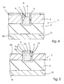
- the exposed surface 7a of the gate conductive region 7 is then oxidised using one of the methods to be described below to form, as illustrated in Figure 4, a protective capping oxide region 9 which is thicker than the gate insulating layer 6.
- the insulating material is then etched back using a conventional etchant so that the exposed region of the gate insulating layer but only a slight thickness of the capping oxide region 9 are removed as shown in Figure 5.
- the oxidation of the gate conductive region 7 may form a capping region 9 of sufficient thickness to provide a suitable step 15 in the surface structure
- the size of this step 15 may be increased by using an appropriate etchant which etches the semiconductor body 1 selectively with respect to the protective capping oxide region 9 to etch back the surface areas 3a of the second region 3 to define a new etched back surface 3b as shown in Figure 5.
- the insulated gate structure 8 extends beyond and thus stands proud of the etched back surface 3b so that areas 8'a of the side walls 8 of the insulated gate structure are exposed and define with the etched back surface areas 3b the step 15 in the surface structure.
- a layer 10 of doped material for example doped polycrystalline silicon or a doped oxide or glass, is then provided using a low temperature deposition technique on the etched back semiconductor surface 3b.
- the doped layer 10 is anisotropically etched to define the doped spacers 10'a as shown in Figure 7 and the structure is then heated to, for example, about 1000°C (degrees Celsius) to cause impurities to diffuse out of the doped spacers 10'a into the underlying portion of the second region 3 to define the third regions 11. If necessary, a short dip etch may then be carried out to remove any slight amount of impurities which may have diffused out of the doped layer 10 into the semiconductor surface 3a before definition of the spacers 10'a.
- the lateral diffusion of the impurities causes the third regions 11 to extend beyond the spacers 10'a so that when the metallisation is deposited as described below to define the first and gate (not shown) electrodes, the first electrode 12 contacts the third regions 11.
- a layer of metallisation is then deposited and patterned to define the first electrode 12 contacting the third regions 11 and shorting the third regions 11 to the second regions to inhibit potential parasitic bipolar action and a second gate electrode (not shown) contacting the insulated gate structure through an appropriate contact window (not shown).
- Another layer 14 of metallisation is provided on the second major surface to form a third electrode contacting the substrate 13.
- the third regions 11 form source regions of the transistor, and the second region 3 defines adjacent the insulated gate structure a conduction channel area 30 within which a conduction channel can be defined by the application of an appropriate voltage to the insulated gate structure 8 to enable conduction between the source region 11 and the second region 3 which forms the drain drift region of the transistor.
- the third electrode forms the drain electrode.
- the situation is similar for an IGBT except that the source 12 and drain electrodes 16 are normally known as the cathode and anode electrodes.
- the present invention requires that the protective capping oxide region 9 formed over the gate conductive region 7 be thicker than the gate insulator so that the gate conductive region 7 remains encapsulated when the exposed areas of the gate insulator are removed.
- This could be achieved simply by relying on the fact that very heavily doped, particularly phosphorus-doped, polycrystalline silicon oxidises much more rapidly than thermal or gate oxide but such a method may be very sensitive to actual process conditions and may not be particularly reproduceable.
- the gate insulating layer may be covered by a layer which is resistant to oxidation.
- the normal gate oxide could be covered by a layer of silicon nitride.
- the gate insulating layer 6 could be formed of a material, other than silicon oxide, which is resistant to oxidation.
- Figures 9 and 10 illustrate one other way of enhancing the oxidation rate of the doped polycrystalline silicon relative to the gate insulating layer 6 where the gate insulating layer is a thermally grown silicon oxide layer.
- the exposed silicon surface is oxidised using conventional techniques to define a thermal gate oxide layer 6.
- the gate oxide layer 6 is then subjected to a nitridation treatment by for example implantation of nitrogen into the gate oxide layer 6 or by heating the semiconductor body in ammonia (both of which techniques are described in a paper entitled selective oxidation technologies for high density MOS by J. Hui, T.Y. Chiu, S. Wong and W.G. Oldham, published in IEEE Electron Device letters Volume EOL.2, No. 10, October 1981 at pages 244 to 247).
- This nitridation treatment results in an oxynitride layer 6' (shown schematically in Figure 10 by way of a dashed line) at the top of the gate oxide layer 6.
- the oxynitride layer is resistant to oxidation so that during the subsequent oxidation of the exposed gate conductive region, the gate oxide layer is not significantly oxidised so resulting in the structure shown in Figure 10.
- the semiconductor device may be a power semiconductor device consisting of many hundreds of parallel-connected source cells with a common drain drift region.
- Figure 11 is a top plan view of part of a semiconductor device manufactured using a method in accordance with the invention with the metallisation forming the source and gate electrodes omitted in order to show the structure.
- the groove 5 is formed as a regular grid-like trench so as to divide the second region 3 into a number of regularly shaped, as shown square, second cell regions 31 each of which is associated with an annular third region 11 bounded by the grid-like trench or groove 5.
- any suitable layout for the geometry of the semiconductor device may be adopted.
- the power semiconductor device may be integrated in the same semiconductor body as various logic components, for example low and/or high voltage lateral transistors, so as to form a power integrated circuit, an intelligent power switch or a smart power device, depending upon the degree and complexity of the integrated logic.
- the present invention may of course be applied to discrete power semiconductor devices and to lateral as well as vertical current flow devices. Furthermore, the present invention may be applied to semiconductor devices, other than power semiconductor devices, which consist of only one or a few insulated gate field effect device cells.
Abstract
The semiconductor body (1) provided in the manufacture of an insulated
gate field effect device comprises a first region (2) of one conductivity type
separated from a major surface (1a) of the body by a second region (3) of the
opposite conductivity type. An insulating gate structure (8) is formed by steps
that include etching the semiconductor body (1) through the window (4a) in a
mask (4) on this major surface (1a) so as to define a groove (5) extending
through the second region (3) into the first region (2), providing a relatively thin
layer of gate insulator (6) on the surface (5a) of the groove (5), providing a
gate conductive region (7) of an oxidisable conductive material within the
groove (5) to define with the gate insulator layer (6) an insulated gate structure
(8) bounded by a conduction channel-defining area (30) of the second region
(3), and causing the insulated gate structure (8) to extend beyond the
surrounding semiconductor surface to define a step (15) in the surface
structure by oxidising the exposed conductive material to define an insulating
capping region (9) over the exposed surface (7a) of the gate conductive region
(7). Thereafter third regions (11) of the one conductivity type are formed in a
self-aligned manner adjacent to the step (15) by providing a doped layer (10)
over the surface structure with the step (15), the doped layer (10) comprising
dopant of the one conductivity type, etching the doped layer (10)
anisotropically to leave portions (10'a) of the doped layer (10) on the sidewall
(8'a) of the step (15) to provide dopant for the third regions (11) and causing
the dopant to diffuse into the underlying part of the second region (3) from the
portions (10'a) of the doped layer (10) left after the anisotropic etching.

Description
This invention relates to a method of manufacturing a semiconductor
device comprising an insulated gate field effect device, in particular an
insulated gate field effect device in which the insulated gate is formed within a
groove or recess.
US-A-4,967,245 describes a so-called trench power MOSFET which is
an insulated gate field effect transistor formed of very many, typically hundreds
of thousands, of parallel-connected insulated gate field effect device cells
(generally referred to as source cells) sharing a common drain region. In the
manufacture of this device as described in US-A-4,967,245 a semiconductor
body is provided having first and second major surfaces and with a region
structure that comprises a first region of one conductivity type separated from
the first major surface by a second region of the opposite conductivity type. An
insulating gate structure is formed by steps that include providing on the one
major surface a mask defining at least one window, etching the semiconductor
body through the window to define a groove extending through the second
region into the first region, providing a relatively thin layer of gate insulator on
the surface of the groove, providing a gate conductive region of an oxidisable
conductive material within the groove to define with the gate insulator layer an
insulated gate structure bounded by a conduction channel-defining area of the
second region, and causing the insulated gate structure to extend beyond the
surrounding semiconductor surface to define a step in the surface structure by
oxidising the exposed conductive material to define an insulating capping
region over the exposed surface of the gate conductive region. Thereafter
third regions of the one conductivity type are formed in the second region
adjacent to the step, and an electrically conductive layer is deposited to
contact both the second and the third regions.
As described in US-A-4,967,245, the third regions are formed by
etching through a layer region of the one conductivity type in the presence of
an etchant mask at the side walls of the step. This etchant mask is defined in
the following self-aligned manner using local oxidation of silicon (LOCOS).
Thus, the mask used to define the groove is formed of a material which resists
oxidation, such as silicon nitride. After the etching back of the polycrystalline
silicon to form the gate conductive region, the exposed surface areas of the
polycrystalline silicon are oxidised to define a protective insulating capping
region over the gate conductive region. As is well known in the semiconductor
art such a local oxidation of silicon (LOCOS) technique results in so-called
oxide bird's beaks at the edges of the anti-oxidation mask, that is areas where
the oxidation proceeds slightly under the edges of the anti-oxidation mask. The
capping region and adjoining bird's beaks regions are then used as a mask to
etch through the layer region to expose the second region leaving third regions
of the one conductivity type beneath the bird's beak region. These third
regions will form the source regions of a power MOSFET while the areas of the
second region adjacent the insulated gate structure will define channel areas
through which conduction occurs when an inversion channel is induced by the
application of an appropriate voltage to the insulated gate. The conductive
layer subsequently deposited then forms the source electrode which contacts
the edges of the source regions defined by the etching process and also
shorts the surrounding areas of the second region to the source regions so as
to avoid parasitic bipolar action.
Although such a method allows the source regions to be formed in a
self-aligned manner and thus allows a reduction in cell size and hence an
increase in cell density, the precise shape and size of the bird's beak regions
depends on the degree to which oxidation occurs under the edges of the anti-oxidation
mask which may depend upon, for example, the degree of adhesion
of the anti-oxidation mask to the first major surface which in turn may depend
upon the surface states and cleanliness of the first major surface. Thus, slight
variations in the LOCOS oxidation process may result in variations in the size
and shape of the bird's beak regions which in turn may affect the size and
shape of the source regions and thus the device characteristics. In addition,
the necessary presence of the anti-oxidation mask on the first major surface
during the formation of the gate insulating layer may result in some
contamination of the gate insulating layer which could affect the device
performance characteristics.
It is an aim of the present invention to provide a method of
manufacturing a semiconductor device comprising an insulated gate field
effect semiconductor device which enables the third regions to be formed in a
self-aligned manner and so allows for an increase in cell packing density
where the device is a power semiconductor device consisting of many parallel-connected
cells without having to rely on the use of so-called birds beak
regions as a mask to define the third regions.
According to the present invention, there is provided a method of
manufacturing a semiconductor device as set out in Claim 1.
Thus, in a method according to the invention, after oxidation of the
exposed surface of the gate conductive region, a portion of the insulated gate
structure stands proud of the semiconductor surface, a doped layer comprising
dopant (also termed "impurities") of the one conductivity type is then deposited
and anisotropically etched to leave portions or spacers on the exposed areas
of the side walls of the insulated gate structure. The spacers are then used to
define the third regions by dopant diffusion into the underlying part of the
second region. The third regions are thus formed so as to be self-aligned to
the insulated gate structure without the need for a local oxidation technique to
define the third regions. This allows the size of the spacers and thus of the
third regions to be determined simply by controlling the thickness of the layer
provided over the surface structure. Moreover, there is no need for an anti-oxidation
mask to be present on the first major surface when the gate
insulating layer is being formed so that the possibilities for contamination of the
gate insulating layer are reduced. In addition because the present invention
does not rely on a local oxidation technique to define the third regions, the
layer which is etched back to define the spacers need not necessarily be an
oxide which should increase the flexibility of the method. This also means that
the semiconductor body need not necessarily be made of a semiconductor,
such as silicon, which is readily oxidisable.
The step of causing the insulated gate structure to extend beyond the
surrounding semiconductor surface to define a step in the surface structure
may further comprise etching back the first major surface using the capping
region as a mask to leave areas of the side wall of the insulated gate structure
exposed and projecting beyond the etched-back surface. This has the
advantage that the step in the surface structure is not determined solely by the
oxidation of the gate conductive region and can be adjusted as desired by
etching away a selected thickness of the semiconductor body.
An anti-oxidation layer may be provided on the first major surface
before forming the gate conductive region. Thus, in one example, the gate
insulator may be formed as an oxide layer covering the first major surface and
the anti-oxidation layer formed by introducing nitrogen to cover at least a
surface region of the gate oxide layer to a nitrogen oxide layer. This provides a
relatively simple way of forming an anti-oxidation layer which is automatically
aligned to the conductive gate region once that is formed. The use of an anti-oxidation
layer facilities selective oxidation of the gate conductive region and
avoids having to rely on the difference in the rates and degrees to which the
gate conductive material and the gate insulating material can be oxidised.
An electrically conductive layer may be provided on the second major
surface so that in operation of the device the main current path is between the
first and second major surfaces through the first region, that is so that the
insulated gate field effect device is a vertical device. The present invention
could however also be applied to lateral devices and to top drain or anode
contact vertical devices.
The insulated gate field effect device may be an insulated gate field
effect transistor or any other MOS-controlled device such as a MOS-gated
thyristor. At least one fourth region of the opposite conductivity type may be
provided spaced from the second region by the first region for injecting charge
carriers of the opposite conductivity type into the first region during operation
of the device so that the insulated gate field effect device forms an insulated
gate bipolar transistor.
The window in the mask may be defined so that the groove forms a
grid-like trench. This has particular advantages in the case of vertical power
insulated gate field effect devices.
It may be noted that published UK patent application GB-A-2 239 561
describes a method of manufacturing a field effect transistor of the insulated
gate electrostatic induction type, in which an accumulation channel of the one
conductivity type is induced in a low-doped drain region of the one conductivity
type. The device has an insulating gate structure formed in a first groove in
the semiconductor body surface and a control gate formed in a second groove
in the same body surface. The insulating gate is formed with a step at the
body surface, over which a layer is deposited and etched back to leave side
wall spacers at the step to act as part of an etchant mask for defining the area
where the second groove is to be etched. Thereby the second groove is
formed in a self-aligned manner with respect to the insulated gate by etching
into the drain region while masking adjacent portions with the side wall
spacers. In one embodiment the deposited layer and resulting side wall
spacers are of doped material comprising dopant of the one conductivity type,
and the source regions of the device are formed by causing the dopant to
diffuse into the underlying un-etched part of the low-doped region of the one
conductivity type.
Embodiments of the invention will now be described, by way of
example, with reference to the accompanying drawings, in which:
It should of course be understood that the drawings are schematic and
are not to scale. Thus, for example, the thickness of various layers or regions
may have been relatively exaggerated in the interests of clarity. Like reference
numerals are used throughout to refer to like parts.
Referring now to the drawings, there are illustrated methods of
manufacturing a semiconductor device comprising an insulated gate field
effect device, which methods comprise providing a semiconductor body 1
having first and second major surfaces 1a and 1b with a first region 2 of one
conductivity type separated from the first major surface 1a by a second region
3 of the opposite conductivity type, providing on the one major surface 1a a
mask 4 defining at least one window 4a, etching the semiconductor body 1
through the window 4a to define a groove 5 extending through the second
region 3 into the first region 2, providing a relatively thin layer of gate insulator
6 on the surface 5a of the groove 5 providing a gate conductive region 7 of an
oxidisable conductive material within the groove 5 to define with the gate
insulator layer an insulated gate structure 8 bounded by a conduction channel-defining
area 30 of the second region 3, causing the insulated gate structure 8
to extend beyond the surrounding semiconductor surface to define a step 15 in
the surface structure by oxidising the exposed 7a gate conductive material to
define an insulating capping region 9 over the exposed surface 7a of the gate
conductive region 3 and then providing a layer 10 over the surface structure,
etching the layer 10 anisotropically to leave portions 10'a of the layer on the
side wall 8a of the step defined by the insulated gate structure 8 and to define
beneath the portions 10'a third regions 11 of the one conductivity type within
the second region 3 by dopant diffusion into the underlying part of the second
region 3. Thereafter an electrically conductive layer 12 is deposited to contact
both the second and the third regions 3 and 11.
Thus, in a method according to the invention, after oxidation of the
exposed surface 7a of the gate conductive region 7, a portion of the insulated
gate structure 8 stands proud of the semiconductor surface 3b, a layer 10 is
then deposited and anisotropically etched to leave portions or spacers 10a on
the exposed areas 8'a of the side walls 8 of the insulated gate structure 8. The
spacers 10'a are then used to define the third regions 11 which are thus
formed so as to be self-aligned to the insulated gate structure 8 without relying
on using a mask defined by a local oxidation technique. This allows the size of
the spacers 10'a and thus of the third regions 11 to be determined simply by
controlling the thickness of the layer 10. In addition, the layer 10 which is
etched back to define the spacers 10'a need not necessarily be an oxide
which should increase the flexibility of the method and, of course, means that
the semiconductor body 1 need not necessarily be made of a semiconductor,
such as silicon, which is readily oxidisable.
An insulated gate field effect device in accordance with the invention
may be, for example, a power MOSFET which consists of many hundreds of
parallel-connected insulated gate field effect transistors having a common
drain region or any other MOS-controlled device such as an insulated gate
bipolar transistor (IGBT).
Figures 1 to 8 are cross-sectional views through part of a
semiconductor body 1 for illustrating an example of a method in accordance
with the invention. It will of course be appreciated that, in the case of a power
device, the structure being formed within the semiconductor body 1 will consist
of many hundreds of parallel identical structures but that, in the interests of
simplicity, only one of these structures is shown.
The semiconductor body 1 consists in this example of a relatively highly
doped single crystal silicon substrate 13 onto which the first region 2 is formed
as an epitaxial layer that is relatively lowly doped with impurities of one
conductivity type. Where the semiconductor device is to be a power MOSFET
then the substrate 13 and first region or epitaxial layer 2 will be of the same
conductivity type, n conductivity type for an n-channel MOSFET, whereas
where the semiconductor device is to be, for example, an IGBT the substrate
13 will be of the opposite conductivity type, p conductivity type in the case of
an n-channel IGBT. The present invention could of course also be applied to
so-called anode-shorted IGBTs as described in, for example, US-A-4969028 in
which the opposite conductivity type injector regions are formed not by an
oppositely doped substrate but by spaced doped injector regions extending
into the relatively highly doped substrate of the one conductivity type from the
second major surface 1b.
The second region 3 that will define the conduction channel regions of
the insulated gate field effect device may be formed either as a second
epitaxial layer of the opposite conductivity type deposited onto the epitaxial
layer 2 or may be formed by introducing impurities of the opposite conductivity
type into the epitaxial layer 2.
As shown in Figure 1, a mask 4 is provided on the first major surface
1a. The mask 4 may be formed of any suitable material, for example,
photosensitive resist, and a window 4a is opened in the mask using
conventional photolithographic and etching techniques to expose an area of
the first major surface 1a.
The exposed semiconductor material is then anisotropically etched to
define a groove 5 extending through the third region 3 into the second region
2.
After removal of the mask 4 and usual surface cleaning, as shown in
Figure 2, a relatively thin layer of gate insulating material 6 is provided on the
first major surface 1a and the surface 5a of the groove 5. The gate insulating
layer 6 is normally formed by a conventional thermal oxidation process carried
out in a special furnace so as to avoid contamination of the gate insulating.
This should result in a high purity gate oxide.
A layer 80 of oxidisable conductive material, in this example heavily
doped, generally phosphorus-doped, polycrystalline silicon, is then provided
over the one major surface using conventional deposition techniques and is
etched back until the surface of the gate insulating layer 6 is exposed thereby
leaving a gate conductive region 7 within the groove 5. As shown in Figure 3,
the doped polycrystalline silicon may be etched back to be level with or slightly
below the first major surface 1a.
The gate conductive region 7 and gate insulating layer 6 together define
an insulated gate structure 8.
The exposed surface 7a of the gate conductive region 7 is then oxidised
using one of the methods to be described below to form, as illustrated in
Figure 4, a protective capping oxide region 9 which is thicker than the gate
insulating layer 6.
The insulating material is then etched back using a conventional
etchant so that the exposed region of the gate insulating layer but only a slight
thickness of the capping oxide region 9 are removed as shown in Figure 5.
Although the oxidation of the gate conductive region 7 may form a
capping region 9 of sufficient thickness to provide a suitable step 15 in the
surface structure, the size of this step 15 may be increased by using an
appropriate etchant which etches the semiconductor body 1 selectively with
respect to the protective capping oxide region 9 to etch back the surface areas
3a of the second region 3 to define a new etched back surface 3b as shown in
Figure 5. In this example, the insulated gate structure 8 extends beyond and
thus stands proud of the etched back surface 3b so that areas 8'a of the side
walls 8 of the insulated gate structure are exposed and define with the etched
back surface areas 3b the step 15 in the surface structure.
In accordance with the invention, as shown in Figure 6, a layer 10 of
doped material, for example doped polycrystalline silicon or a doped oxide or
glass, is then provided using a low temperature deposition technique on the
etched back semiconductor surface 3b.
The doped layer 10 is anisotropically etched to define the doped
spacers 10'a as shown in Figure 7 and the structure is then heated to, for
example, about 1000°C (degrees Celsius) to cause impurities to diffuse out of
the doped spacers 10'a into the underlying portion of the second region 3 to
define the third regions 11. If necessary, a short dip etch may then be carried
out to remove any slight amount of impurities which may have diffused out of
the doped layer 10 into the semiconductor surface 3a before definition of the
spacers 10'a.
As can be seen from Figure 7, the lateral diffusion of the impurities
causes the third regions 11 to extend beyond the spacers 10'a so that when
the metallisation is deposited as described below to define the first and gate
(not shown) electrodes, the first electrode 12 contacts the third regions 11.
A layer of metallisation, generally aluminum, is then deposited and
patterned to define the first electrode 12 contacting the third regions 11 and
shorting the third regions 11 to the second regions to inhibit potential parasitic
bipolar action and a second gate electrode (not shown) contacting the
insulated gate structure through an appropriate contact window (not shown).
Another layer 14 of metallisation is provided on the second major surface to
form a third electrode contacting the substrate 13.
Where the semiconductor device is an insulated gate field effect
transistor then the third regions 11 form source regions of the transistor, and
the second region 3 defines adjacent the insulated gate structure a conduction
channel area 30 within which a conduction channel can be defined by the
application of an appropriate voltage to the insulated gate structure 8 to enable
conduction between the source region 11 and the second region 3 which
forms the drain drift region of the transistor. In this case the third electrode
forms the drain electrode. The situation is similar for an IGBT except that the
source 12 and drain electrodes 16 are normally known as the cathode and
anode electrodes.
As will be appreciated from the above description, the present invention
requires that the protective capping oxide region 9 formed over the gate
conductive region 7 be thicker than the gate insulator so that the gate
conductive region 7 remains encapsulated when the exposed areas of the
gate insulator are removed. This could be achieved simply by relying on the
fact that very heavily doped, particularly phosphorus-doped, polycrystalline
silicon oxidises much more rapidly than thermal or gate oxide but such a
method may be very sensitive to actual process conditions and may not be
particularly reproduceable. Alternatively, the gate insulating layer may be
covered by a layer which is resistant to oxidation. Thus, for example, the
normal gate oxide could be covered by a layer of silicon nitride. As another
example the gate insulating layer 6 could be formed of a material, other than
silicon oxide, which is resistant to oxidation.
Figures 9 and 10 illustrate one other way of enhancing the oxidation
rate of the doped polycrystalline silicon relative to the gate insulating layer 6
where the gate insulating layer is a thermally grown silicon oxide layer.
Thus, as illustrated in Figure 9, after removal of the mask 4, the
exposed silicon surface is oxidised using conventional techniques to define a
thermal gate oxide layer 6. The gate oxide layer 6 is then subjected to a
nitridation treatment by for example implantation of nitrogen into the gate oxide
layer 6 or by heating the semiconductor body in ammonia (both of which
techniques are described in a paper entitled selective oxidation technologies
for high density MOS by J. Hui, T.Y. Chiu, S. Wong and W.G. Oldham,
published in IEEE Electron Device letters Volume EOL.2, No. 10, October
1981 at pages 244 to 247).
This nitridation treatment results in an oxynitride layer 6' (shown
schematically in Figure 10 by way of a dashed line) at the top of the gate oxide
layer 6. The oxynitride layer is resistant to oxidation so that during the
subsequent oxidation of the exposed gate conductive region, the gate oxide
layer is not significantly oxidised so resulting in the structure shown in Figure
10.
The remainder of the process may continue as described above with
reference to Figures 1 to 8.
As indicated above, the semiconductor device may be a power
semiconductor device consisting of many hundreds of parallel-connected
source cells with a common drain drift region.
Figure 11 is a top plan view of part of a semiconductor device
manufactured using a method in accordance with the invention with the
metallisation forming the source and gate electrodes omitted in order to show
the structure.
As can be seen from Figure 11, the groove 5 is formed as a regular
grid-like trench so as to divide the second region 3 into a number of regularly
shaped, as shown square, second cell regions 31 each of which is associated
with an annular third region 11 bounded by the grid-like trench or groove 5. Of
course, any suitable layout for the geometry of the semiconductor device may
be adopted.
The power semiconductor device may be integrated in the same
semiconductor body as various logic components, for example low and/or high
voltage lateral transistors, so as to form a power integrated circuit, an
intelligent power switch or a smart power device, depending upon the degree
and complexity of the integrated logic.
The present invention may of course be applied to discrete power
semiconductor devices and to lateral as well as vertical current flow devices.
Furthermore, the present invention may be applied to semiconductor devices,
other than power semiconductor devices, which consist of only one or a few
insulated gate field effect device cells.
From reading the present disclosure, other modifications and variations
will be apparent to persons skilled in the art. Such modifications and variations
may involve other features which are already known in the semiconductor art
and which may be used instead of or in addition to features already described
herein.
It has been stated above that the drawings illustrate examples of
embodiments of the invention and, in order to avoid any misunderstanding, it is
hereby further stated that, in the following claims, where technical features
mentioned in any claim are followed by reference signs relating to features in
the drawings and placed between parentheses, these reference signs have
been included in accordance with Rule 29(7) EPC for the sole purpose of
facilitating comprehension of the claim, by reference to an example.
The present application is a divisional from European patent application
94200834.3 (published as EP-A-0 620 588), the whole contents of which are
hereby incorporated herein as additional reference material for further
understanding the present invention.
Claims (10)
- A method of manufacturing a semiconductor device comprising an insulated gate field effect device, wherein a semiconductor body (1) is provided having first and second major surfaces (1a, 1b) and with a region structure that comprises a first region (2) of one conductivity type separated from the first major surface (1a) by a second region (3) of the opposite conductivity type, and an insulating gate structure (8) is formed by steps that include providing on the one major surface (1a) a mask (4) defining at least one window (4a), etching the semiconductor body (1) through the window (4a) to define a groove (5) extending through the second region (3) into the first region (2), providing a relatively thin layer of gate insulator (6) on the surface (5a) of the groove (5), providing a gate conductive region (7) of an oxidisable conductive material within the groove (5) to define with the gate insulator layer (6) an insulated gate structure (8) bounded by a conduction channel-defining area (30) of the second region (3), and causing the insulated gate structure (8) to extend beyond the surrounding semiconductor surface to define a step (15) in the surface structure by oxidising the exposed conductive material to define an insulating capping region (9) over the exposed surface (7a) of the gate conductive region (7), after which third regions (11) of the one conductivity type are formed in the second region (3) adjacent to the step (15), and an electrically conductive layer (12) is deposited to contact both the second and the third regions (3, 11), which method is characterised in that the third regions (11) are formed by providing a doped layer (10) over the surface structure with the step (15), the doped layer (10) comprising dopant of the one conductivity type, etching the doped layer (10) anisotropically to leave portions (10'a) of the doped layer (10) on the sidewall (8'a) of the step (15) to provide dopant for the third regions (11) and causing the dopant to diffuse into the underlying part of the second region (3) from the portions (10'a) of the doped layer (10) left after the anisotropic etching.
- A method according to Claim 1, wherein the doped layer (10) is a layer of doped polycrystalline silicon.
- A method according to Claim 1, wherein the doped layer (10) is a layer of doped oxide or glass.
- A method according to any one of the preceding Claims, wherein the portions (10'a) of the doped layer (10) on the sidewall (8'a) of the step (15) are retained in the manufactured device.
- A method according to any one of the preceding Claims, wherein a dip etch of the semiconductor surface (3b) is carried out after diffusing the dopant from the portions (10a) of the doped layer (10).
- A method according to any one of the preceding Claims, wherein the gate conductive region (7) is formed of doped polycrystalline silicon, and an anti-oxidation layer (6') is provided on the first major surface (1a) before forming the gate conductive region (7).
- A method according to Claim 6, wherein the gate insulator (6) is formed as an oxide layer covering the first major surface (1a), and the anti-oxidation layer (6') is formed by introducing nitrogen to convert at least a surface region of the gate oxide layer (6) to a nitrogen oxide layer (6').
- A method according to any one of the preceding Claims, wherein the step of causing the insulated gate structure (8) to extend beyond the surrounding semiconductor surface to define the step (15) in the surface structure further comprises etching back the first major surface (1a) using the capping region (9) as a mask to leave areas (8'a) of the side walls (8a) of the insulated gate structure (8) exposed and projecting beyond the etched-back surface (3b).
- A method according to any one of the preceding claims, wherein there is provided at least one fourth region (13) of the opposite conductivity type spaced from the second region (3) by the first region (2) for injecting charge carriers of the opposite conductivity type into the first region (2) during operation of the device.
- A method according to any one of the preceding claims, which comprises defining the window (4a) in the mask (4) so that the groove (5) forms a grid-like trench.
Applications Claiming Priority (3)
| Application Number | Priority Date | Filing Date | Title |
|---|---|---|---|
| GB939306895A GB9306895D0 (en) | 1993-04-01 | 1993-04-01 | A method of manufacturing a semiconductor device comprising an insulated gate field effect device |
| GB9306895 | 1993-04-01 | ||
| EP94200834A EP0620588B1 (en) | 1993-04-01 | 1994-03-29 | A method of manufacturing a recessed insulated gate field-effect semiconductor device |
Related Parent Applications (2)
| Application Number | Title | Priority Date | Filing Date |
|---|---|---|---|
| EP94200834A Division EP0620588B1 (en) | 1993-04-01 | 1994-03-29 | A method of manufacturing a recessed insulated gate field-effect semiconductor device |
| EP94200834.3 Division | 1994-03-29 |
Publications (1)
| Publication Number | Publication Date |
|---|---|
| EP0918353A1 true EP0918353A1 (en) | 1999-05-26 |
Family
ID=10733222
Family Applications (2)
| Application Number | Title | Priority Date | Filing Date |
|---|---|---|---|
| EP99200133A Withdrawn EP0918353A1 (en) | 1993-04-01 | 1994-03-29 | A method of manufacturing a recessed insulated gate field-effect semiconductor device |
| EP94200834A Expired - Lifetime EP0620588B1 (en) | 1993-04-01 | 1994-03-29 | A method of manufacturing a recessed insulated gate field-effect semiconductor device |
Family Applications After (1)
| Application Number | Title | Priority Date | Filing Date |
|---|---|---|---|
| EP94200834A Expired - Lifetime EP0620588B1 (en) | 1993-04-01 | 1994-03-29 | A method of manufacturing a recessed insulated gate field-effect semiconductor device |
Country Status (6)
| Country | Link |
|---|---|
| US (1) | US5378655A (en) |
| EP (2) | EP0918353A1 (en) |
| JP (1) | JPH06350090A (en) |
| KR (1) | KR100296805B1 (en) |
| DE (1) | DE69434948D1 (en) |
| GB (1) | GB9306895D0 (en) |
Cited By (1)
| Publication number | Priority date | Publication date | Assignee | Title |
|---|---|---|---|---|
| CN105304626A (en) * | 2014-07-23 | 2016-02-03 | 意法半导体(图尔)公司 | Bidirectional switch |
Families Citing this family (72)
| Publication number | Priority date | Publication date | Assignee | Title |
|---|---|---|---|---|
| US5283201A (en) * | 1988-05-17 | 1994-02-01 | Advanced Power Technology, Inc. | High density power device fabrication process |
| US6603173B1 (en) | 1991-07-26 | 2003-08-05 | Denso Corporation | Vertical type MOSFET |
| JP3481287B2 (en) * | 1994-02-24 | 2003-12-22 | 三菱電機株式会社 | Manufacturing method of semiconductor device |
| US5583065A (en) * | 1994-11-23 | 1996-12-10 | Sony Corporation | Method of making a MOS semiconductor device |
| JP3319215B2 (en) * | 1995-03-31 | 2002-08-26 | 株式会社豊田中央研究所 | Insulated gate semiconductor device and method of manufacturing the same |
| US5567634A (en) * | 1995-05-01 | 1996-10-22 | National Semiconductor Corporation | Method of fabricating self-aligned contact trench DMOS transistors |
| US5648670A (en) * | 1995-06-07 | 1997-07-15 | Sgs-Thomson Microelectronics, Inc. | Trench MOS-gated device with a minimum number of masks |
| JPH11204782A (en) * | 1998-01-08 | 1999-07-30 | Toshiba Corp | Semiconductor device and manufacture therefor |
| US6097061A (en) * | 1998-03-30 | 2000-08-01 | Advanced Micro Devices, Inc. | Trenched gate metal oxide semiconductor device and method |
| US6285054B1 (en) | 1998-03-30 | 2001-09-04 | Advanced Micro Devices, Inc. | Trenched gate non-volatile semiconductor device with the source/drain regions spaced from the trench by sidewall dopings |
| US6225659B1 (en) | 1998-03-30 | 2001-05-01 | Advanced Micro Devices, Inc. | Trenched gate semiconductor device and method for low power applications |
| GB9808237D0 (en) * | 1998-04-17 | 1998-06-17 | Koninkl Philips Electronics Nv | Mnufacture of field-effect semiconductor devices |
| GB9808234D0 (en) * | 1998-04-17 | 1998-06-17 | Koninkl Philips Electronics Nv | Mnufacture of trench-gate semiconductor devices |
| GB9815021D0 (en) | 1998-07-11 | 1998-09-09 | Koninkl Philips Electronics Nv | Semiconductor power device manufacture |
| EP0981166A3 (en) * | 1998-08-17 | 2000-04-19 | ELMOS Semiconductor AG | JFET transistor |
| US6084264A (en) * | 1998-11-25 | 2000-07-04 | Siliconix Incorporated | Trench MOSFET having improved breakdown and on-resistance characteristics |
| GB9826041D0 (en) | 1998-11-28 | 1999-01-20 | Koninkl Philips Electronics Nv | Trench-gate semiconductor devices and their manufacture |
| JP3924975B2 (en) * | 1999-02-05 | 2007-06-06 | 富士電機デバイステクノロジー株式会社 | Trench type insulated gate bipolar transistor |
| GB9906247D0 (en) | 1999-03-18 | 1999-05-12 | Koninkl Philips Electronics Nv | An electronic device comprising a trench gate field effect device |
| GB9907184D0 (en) | 1999-03-30 | 1999-05-26 | Philips Electronics Nv | A method of manufacturing a semiconductor device |
| US6373098B1 (en) * | 1999-05-25 | 2002-04-16 | Fairchild Semiconductor Corporation | Trench-gated device having trench walls formed by selective epitaxial growth and process for forming device |
| GB9922764D0 (en) | 1999-09-28 | 1999-11-24 | Koninkl Philips Electronics Nv | Manufacture of trench-gate semiconductor devices |
| GB9928285D0 (en) | 1999-11-30 | 2000-01-26 | Koninkl Philips Electronics Nv | Manufacture of trench-gate semiconductor devices |
| US6921939B2 (en) * | 2000-07-20 | 2005-07-26 | Fairchild Semiconductor Corporation | Power MOSFET and method for forming same using a self-aligned body implant |
| GB0101695D0 (en) | 2001-01-23 | 2001-03-07 | Koninkl Philips Electronics Nv | Manufacture of trench-gate semiconductor devices |
| US7132712B2 (en) * | 2002-11-05 | 2006-11-07 | Fairchild Semiconductor Corporation | Trench structure having one or more diodes embedded therein adjacent a PN junction |
| JP4932088B2 (en) | 2001-02-19 | 2012-05-16 | ルネサスエレクトロニクス株式会社 | Insulated gate type semiconductor device manufacturing method |
| US7061066B2 (en) | 2001-10-17 | 2006-06-13 | Fairchild Semiconductor Corporation | Schottky diode using charge balance structure |
| US8080459B2 (en) * | 2002-09-24 | 2011-12-20 | Vishay-Siliconix | Self aligned contact in a semiconductor device and method of fabricating the same |
| US8629019B2 (en) | 2002-09-24 | 2014-01-14 | Vishay-Siliconix | Method of forming self aligned contacts for a power MOSFET |
| KR100511590B1 (en) * | 2003-01-30 | 2005-09-02 | 동부아남반도체 주식회사 | Semiconductor device and method for fabrication thereof |
| US7352036B2 (en) | 2004-08-03 | 2008-04-01 | Fairchild Semiconductor Corporation | Semiconductor power device having a top-side drain using a sinker trench |
| US7667264B2 (en) * | 2004-09-27 | 2010-02-23 | Alpha And Omega Semiconductor Limited | Shallow source MOSFET |
| US7948029B2 (en) | 2005-02-11 | 2011-05-24 | Alpha And Omega Semiconductor Incorporated | MOS device with varying trench depth |
| US8362547B2 (en) | 2005-02-11 | 2013-01-29 | Alpha & Omega Semiconductor Limited | MOS device with Schottky barrier controlling layer |
| US8283723B2 (en) * | 2005-02-11 | 2012-10-09 | Alpha & Omega Semiconductor Limited | MOS device with low injection diode |
| US8093651B2 (en) | 2005-02-11 | 2012-01-10 | Alpha & Omega Semiconductor Limited | MOS device with integrated schottky diode in active region contact trench |
| US7285822B2 (en) * | 2005-02-11 | 2007-10-23 | Alpha & Omega Semiconductor, Inc. | Power MOS device |
| CN101882583A (en) * | 2005-04-06 | 2010-11-10 | 飞兆半导体公司 | Trenched-gate field effect transistors and forming method thereof |
| US7488647B1 (en) * | 2005-08-11 | 2009-02-10 | National Semiconductor Corporation | System and method for providing a poly cap and a no field oxide area to prevent formation of a vertical bird's beak structure in the manufacture of a semiconductor device |
| US7544545B2 (en) | 2005-12-28 | 2009-06-09 | Vishay-Siliconix | Trench polysilicon diode |
| WO2007084688A1 (en) | 2006-01-18 | 2007-07-26 | Vishay-Siliconix | Floating gate structure with high electrostatic discharge performance |
| US7446374B2 (en) * | 2006-03-24 | 2008-11-04 | Fairchild Semiconductor Corporation | High density trench FET with integrated Schottky diode and method of manufacture |
| DE102006030631B4 (en) * | 2006-07-03 | 2011-01-05 | Infineon Technologies Austria Ag | Semiconductor device arrangement with a power component and a logic device |
| DE102006047244B4 (en) * | 2006-10-04 | 2018-01-18 | Infineon Technologies Austria Ag | Semiconductor device with a monocrystalline semiconductor body and method for producing the same |
| US7531888B2 (en) * | 2006-11-30 | 2009-05-12 | Fairchild Semiconductor Corporation | Integrated latch-up free insulated gate bipolar transistor |
| TWI360864B (en) * | 2006-12-06 | 2012-03-21 | Promos Technologies Inc | Gate structure and method of fabriacting the same, |
| US9437729B2 (en) | 2007-01-08 | 2016-09-06 | Vishay-Siliconix | High-density power MOSFET with planarized metalization |
| US9947770B2 (en) | 2007-04-03 | 2018-04-17 | Vishay-Siliconix | Self-aligned trench MOSFET and method of manufacture |
| US20080296673A1 (en) * | 2007-05-29 | 2008-12-04 | Alpha & Omega Semiconductor, Ltd | Double gate manufactured with locos techniques |
| US9484451B2 (en) | 2007-10-05 | 2016-11-01 | Vishay-Siliconix | MOSFET active area and edge termination area charge balance |
| US10600902B2 (en) | 2008-02-13 | 2020-03-24 | Vishay SIliconix, LLC | Self-repairing field effect transisitor |
| US20090242973A1 (en) | 2008-03-31 | 2009-10-01 | Alpha & Omega Semiconductor, Ltd. | Source and body contact structure for trench-dmos devices using polysilicon |
| US7867852B2 (en) * | 2008-08-08 | 2011-01-11 | Alpha And Omega Semiconductor Incorporated | Super-self-aligned trench-dmos structure and method |
| US8426275B2 (en) * | 2009-01-09 | 2013-04-23 | Niko Semiconductor Co., Ltd. | Fabrication method of trenched power MOSFET |
| JP5472862B2 (en) * | 2009-03-17 | 2014-04-16 | 三菱電機株式会社 | Method for manufacturing power semiconductor device |
| US9425306B2 (en) | 2009-08-27 | 2016-08-23 | Vishay-Siliconix | Super junction trench power MOSFET devices |
| US9443974B2 (en) | 2009-08-27 | 2016-09-13 | Vishay-Siliconix | Super junction trench power MOSFET device fabrication |
| US9230810B2 (en) | 2009-09-03 | 2016-01-05 | Vishay-Siliconix | System and method for substrate wafer back side and edge cross section seals |
| US9431530B2 (en) | 2009-10-20 | 2016-08-30 | Vishay-Siliconix | Super-high density trench MOSFET |
| JP5662865B2 (en) | 2010-05-19 | 2015-02-04 | ルネサスエレクトロニクス株式会社 | Semiconductor device and manufacturing method thereof |
| US9431249B2 (en) | 2011-12-01 | 2016-08-30 | Vishay-Siliconix | Edge termination for super junction MOSFET devices |
| US9614043B2 (en) | 2012-02-09 | 2017-04-04 | Vishay-Siliconix | MOSFET termination trench |
| CN103367145A (en) * | 2012-03-27 | 2013-10-23 | 北大方正集团有限公司 | Trench VDMOS device and manufacturing method thereof |
| US9842911B2 (en) | 2012-05-30 | 2017-12-12 | Vishay-Siliconix | Adaptive charge balanced edge termination |
| JP5622814B2 (en) * | 2012-08-29 | 2014-11-12 | 三菱電機株式会社 | Semiconductor device and manufacturing method thereof |
| US9508596B2 (en) | 2014-06-20 | 2016-11-29 | Vishay-Siliconix | Processes used in fabricating a metal-insulator-semiconductor field effect transistor |
| US9887259B2 (en) | 2014-06-23 | 2018-02-06 | Vishay-Siliconix | Modulated super junction power MOSFET devices |
| KR102026543B1 (en) | 2014-08-19 | 2019-09-27 | 비쉐이-실리코닉스 | Electronic circuit |
| KR102098996B1 (en) | 2014-08-19 | 2020-04-08 | 비쉐이-실리코닉스 | Super-junction metal oxide semiconductor field effect transistor |
| CN106898549A (en) * | 2015-12-21 | 2017-06-27 | 株洲南车时代电气股份有限公司 | Trench gate IGBT and trench gate IGBT preparation methods |
| CN114093768A (en) * | 2022-01-20 | 2022-02-25 | 威海银创微电子技术有限公司 | Method and device for protecting Gate in Trench VDMOS, electronic equipment and medium |
Citations (3)
| Publication number | Priority date | Publication date | Assignee | Title |
|---|---|---|---|---|
| EP0238749A2 (en) * | 1986-03-24 | 1987-09-30 | SILICONIX Incorporated | Groove gate unipolar and bipolar MOS devices and method of manufacturing the same |
| US4967245A (en) * | 1988-03-14 | 1990-10-30 | Siliconix Incorporated | Trench power MOSFET device |
| GB2239561A (en) * | 1989-12-28 | 1991-07-03 | Nissan Motor | Method of manufacturing field effect transistors |
Family Cites Families (8)
| Publication number | Priority date | Publication date | Assignee | Title |
|---|---|---|---|---|
| JPH0783118B2 (en) * | 1988-06-08 | 1995-09-06 | 三菱電機株式会社 | Semiconductor device and manufacturing method thereof |
| JPH023980A (en) * | 1988-06-22 | 1990-01-09 | Nissan Motor Co Ltd | Perpendicular field effect transistor |
| JP2689606B2 (en) * | 1989-05-24 | 1997-12-10 | 富士電機株式会社 | Method for manufacturing insulated gate field effect transistor |
| US4992390A (en) * | 1989-07-06 | 1991-02-12 | General Electric Company | Trench gate structure with thick bottom oxide |
| JP2606404B2 (en) * | 1990-04-06 | 1997-05-07 | 日産自動車株式会社 | Semiconductor device |
| KR940002400B1 (en) * | 1991-05-15 | 1994-03-24 | 금성일렉트론 주식회사 | Manufacturing method of semiconductor device with recess gate |
| JP2837014B2 (en) * | 1992-02-17 | 1998-12-14 | 三菱電機株式会社 | Semiconductor device and manufacturing method thereof |
| US5275965A (en) * | 1992-11-25 | 1994-01-04 | Micron Semiconductor, Inc. | Trench isolation using gated sidewalls |
-
1993
- 1993-04-01 GB GB939306895A patent/GB9306895D0/en active Pending
-
1994
- 1994-03-29 DE DE69434948T patent/DE69434948D1/en not_active Expired - Lifetime
- 1994-03-29 EP EP99200133A patent/EP0918353A1/en not_active Withdrawn
- 1994-03-29 EP EP94200834A patent/EP0620588B1/en not_active Expired - Lifetime
- 1994-03-31 US US08/221,293 patent/US5378655A/en not_active Expired - Lifetime
- 1994-03-31 JP JP6063339A patent/JPH06350090A/en active Pending
- 1994-03-31 KR KR1019940006662A patent/KR100296805B1/en not_active IP Right Cessation
Patent Citations (3)
| Publication number | Priority date | Publication date | Assignee | Title |
|---|---|---|---|---|
| EP0238749A2 (en) * | 1986-03-24 | 1987-09-30 | SILICONIX Incorporated | Groove gate unipolar and bipolar MOS devices and method of manufacturing the same |
| US4967245A (en) * | 1988-03-14 | 1990-10-30 | Siliconix Incorporated | Trench power MOSFET device |
| GB2239561A (en) * | 1989-12-28 | 1991-07-03 | Nissan Motor | Method of manufacturing field effect transistors |
Non-Patent Citations (1)
| Title |
|---|
| KRISHNA SHENAI: "OPTIMIZED TRENCH MOSFET TECHNOLOGIES FOR POWER DEVICES", IEEE TRANSACTIONS ON ELECTRON DEVICES, vol. 39, no. 6, 1 June 1992 (1992-06-01), pages 1435 - 1443, XP000271790 * |
Cited By (2)
| Publication number | Priority date | Publication date | Assignee | Title |
|---|---|---|---|---|
| CN105304626A (en) * | 2014-07-23 | 2016-02-03 | 意法半导体(图尔)公司 | Bidirectional switch |
| CN105304626B (en) * | 2014-07-23 | 2018-11-02 | 意法半导体(图尔)公司 | Two-way switch |
Also Published As
| Publication number | Publication date |
|---|---|
| EP0620588A3 (en) | 1996-08-14 |
| EP0620588A2 (en) | 1994-10-19 |
| KR100296805B1 (en) | 2001-11-30 |
| US5378655A (en) | 1995-01-03 |
| EP0620588B1 (en) | 2007-04-11 |
| JPH06350090A (en) | 1994-12-22 |
| GB9306895D0 (en) | 1993-05-26 |
| DE69434948D1 (en) | 2007-05-24 |
Similar Documents
| Publication | Publication Date | Title |
|---|---|---|
| US5378655A (en) | Method of manufacturing a semiconductor device comprising an insulated gate field effect device | |
| US6498071B2 (en) | Manufacture of trench-gate semiconductor devices | |
| EP1393362B1 (en) | Method of manufacturing a trench-gate semiconductor device | |
| US4258465A (en) | Method for fabrication of offset gate MIS device | |
| US5970329A (en) | Method of forming power semiconductor devices having insulated gate electrodes | |
| US5798549A (en) | Conductive layer overlaid self-aligned MOS-gated semiconductor devices | |
| US6660591B2 (en) | Trench-gate semiconductor devices having a channel-accommodating region and their methods of manufacture | |
| JP2001189456A (en) | Vertical mos transistor and manufacturing method therefor | |
| US6087224A (en) | Manufacture of trench-gate semiconductor devices | |
| JP2004538626A (en) | Output MOSFET with deep injection junction | |
| KR100272051B1 (en) | Process for manufacture of a p-channel mos gated device with base implant through the contact window | |
| JPH07249770A (en) | Semiconductor device and its fabrication | |
| JP2002026323A (en) | Method of manufacturing trench gate type mis device having thick polysilicon insulating layer at bottom of trench | |
| JP3502509B2 (en) | Integrated circuit having CMOS structure and method of manufacturing the same | |
| KR100253261B1 (en) | Fabrication method of thin film transistor | |
| KR100192973B1 (en) | Power mos device with inclined gate oxide and manufacturing method thereof | |
| KR19990051079A (en) | Manufacturing Method of Power Device Using Insulating Film Inclined Etching | |
| JPS63227059A (en) | Semiconductor device and manufacture thereof | |
| KR960013945B1 (en) | Soi transistor structure | |
| JP2789998B2 (en) | Semiconductor device | |
| KR910009742B1 (en) | High voltage semiconductor device and its manufacturing method | |
| JPH0571191B2 (en) | ||
| JP2001515658A (en) | Contact arrangement for an integrable planar semiconductor device and method of forming the contact arrangement | |
| JPH08107206A (en) | Semiconductor device and its manufacture | |
| KR19990057296A (en) | Method for manufacturing semiconductor device having non-uniform gate oxide film thickness |
Legal Events
| Date | Code | Title | Description |
|---|---|---|---|
| PUAI | Public reference made under article 153(3) epc to a published international application that has entered the european phase |
Free format text: ORIGINAL CODE: 0009012 |
|
| AC | Divisional application: reference to earlier application |
Ref document number: 620588 Country of ref document: EP |
|
| AK | Designated contracting states |
Kind code of ref document: A1 Designated state(s): DE FR GB IT |
|
| 17P | Request for examination filed |
Effective date: 19991126 |
|
| 17Q | First examination report despatched |
Effective date: 20011228 |
|
| STAA | Information on the status of an ep patent application or granted ep patent |
Free format text: STATUS: THE APPLICATION IS DEEMED TO BE WITHDRAWN |
|
| 18D | Application deemed to be withdrawn |
Effective date: 20020709 |