EP0906007B1 - Multi-pin connector - Google Patents
Multi-pin connector Download PDFInfo
- Publication number
- EP0906007B1 EP0906007B1 EP98305772A EP98305772A EP0906007B1 EP 0906007 B1 EP0906007 B1 EP 0906007B1 EP 98305772 A EP98305772 A EP 98305772A EP 98305772 A EP98305772 A EP 98305772A EP 0906007 B1 EP0906007 B1 EP 0906007B1
- Authority
- EP
- European Patent Office
- Prior art keywords
- base
- grid array
- pin grid
- electrical
- fingers
- Prior art date
- Legal status (The legal status is an assumption and is not a legal conclusion. Google has not performed a legal analysis and makes no representation as to the accuracy of the status listed.)
- Expired - Lifetime
Links
Images
Classifications
-
- H—ELECTRICITY
- H01—ELECTRIC ELEMENTS
- H01R—ELECTRICALLY-CONDUCTIVE CONNECTIONS; STRUCTURAL ASSOCIATIONS OF A PLURALITY OF MUTUALLY-INSULATED ELECTRICAL CONNECTING ELEMENTS; COUPLING DEVICES; CURRENT COLLECTORS
- H01R13/00—Details of coupling devices of the kinds covered by groups H01R12/70 or H01R24/00 - H01R33/00
- H01R13/02—Contact members
- H01R13/22—Contacts for co-operating by abutting
- H01R13/24—Contacts for co-operating by abutting resilient; resiliently-mounted
- H01R13/2442—Contacts for co-operating by abutting resilient; resiliently-mounted with a single cantilevered beam
-
- H—ELECTRICITY
- H01—ELECTRIC ELEMENTS
- H01R—ELECTRICALLY-CONDUCTIVE CONNECTIONS; STRUCTURAL ASSOCIATIONS OF A PLURALITY OF MUTUALLY-INSULATED ELECTRICAL CONNECTING ELEMENTS; COUPLING DEVICES; CURRENT COLLECTORS
- H01R12/00—Structural associations of a plurality of mutually-insulated electrical connecting elements, specially adapted for printed circuits, e.g. printed circuit boards [PCB], flat or ribbon cables, or like generally planar structures, e.g. terminal strips, terminal blocks; Coupling devices specially adapted for printed circuits, flat or ribbon cables, or like generally planar structures; Terminals specially adapted for contact with, or insertion into, printed circuits, flat or ribbon cables, or like generally planar structures
- H01R12/70—Coupling devices
- H01R12/71—Coupling devices for rigid printing circuits or like structures
- H01R12/712—Coupling devices for rigid printing circuits or like structures co-operating with the surface of the printed circuit or with a coupling device exclusively provided on the surface of the printed circuit
- H01R12/714—Coupling devices for rigid printing circuits or like structures co-operating with the surface of the printed circuit or with a coupling device exclusively provided on the surface of the printed circuit with contacts abutting directly the printed circuit; Button contacts therefore provided on the printed circuit
-
- H—ELECTRICITY
- H05—ELECTRIC TECHNIQUES NOT OTHERWISE PROVIDED FOR
- H05K—PRINTED CIRCUITS; CASINGS OR CONSTRUCTIONAL DETAILS OF ELECTRIC APPARATUS; MANUFACTURE OF ASSEMBLAGES OF ELECTRICAL COMPONENTS
- H05K7/00—Constructional details common to different types of electric apparatus
- H05K7/02—Arrangements of circuit components or wiring on supporting structure
- H05K7/10—Plug-in assemblages of components, e.g. IC sockets
- H05K7/1053—Plug-in assemblages of components, e.g. IC sockets having interior leads
- H05K7/1076—Plug-in assemblages of components, e.g. IC sockets having interior leads co-operating by sliding
- H05K7/1084—Plug-in assemblages of components, e.g. IC sockets having interior leads co-operating by sliding pin grid array package carriers
-
- H—ELECTRICITY
- H01—ELECTRIC ELEMENTS
- H01R—ELECTRICALLY-CONDUCTIVE CONNECTIONS; STRUCTURAL ASSOCIATIONS OF A PLURALITY OF MUTUALLY-INSULATED ELECTRICAL CONNECTING ELEMENTS; COUPLING DEVICES; CURRENT COLLECTORS
- H01R12/00—Structural associations of a plurality of mutually-insulated electrical connecting elements, specially adapted for printed circuits, e.g. printed circuit boards [PCB], flat or ribbon cables, or like generally planar structures, e.g. terminal strips, terminal blocks; Coupling devices specially adapted for printed circuits, flat or ribbon cables, or like generally planar structures; Terminals specially adapted for contact with, or insertion into, printed circuits, flat or ribbon cables, or like generally planar structures
- H01R12/50—Fixed connections
- H01R12/51—Fixed connections for rigid printed circuits or like structures
- H01R12/52—Fixed connections for rigid printed circuits or like structures connecting to other rigid printed circuits or like structures
Definitions
- the present invention pertains generally to electrical connectors. More specifically, the present invention pertains to deflection beam electrical connectors which project from a base member to establish electrical contact between electrical devices. The present invention is particularly, but not exclusively, useful for establishing a plethora of electrical circuits between electrical devices.
- a pin grid array will include a generally flat base member, and will have a multitude of individual electrical connectors. For most applications, these connectors are mounted as an array on the base member and extend from both sides thereof to establish as many different electrical pathways through the base member of the array.
- a commonly used component for the individual electrical connectors of a pin grid array is a deformable, electrically conductive, wire mesh structure known as a "fuzz button".
- fuzz button In addition to establishing an electrical pathway, an important attribute of these so-called fuzz buttons is that they are inherently resilient and flexible. This resilience and flexibility, however, can be both beneficial and detrimental to the performance of the pin grid array.
- resilience and flexibility in an electrical connector are desirable in that these qualities promote the proper engagement of an electrical connector with an electrical device. For instance, some relative movement between the connector and the device is beneficial for causing a "wiping" action which helps assure electrical contact between the device and the connector, and thereby establish the electrical pathway through the connector. Further, some flexibility between electrical components is advantageous in order to accommodate variations in the tolerances that are engineered into electrical devices.
- fuzz buttons are generally highly deformable, and easily accommodate tolerance variations, they can become misshapen with extended repetitive use. Thus, they are prone to giving uneven contact pressures between the various electrical contact points. For the same reason, fuzz buttons are prone to loosing their registration with the contact points on the electrical connector to which they are mated. With either uneven contact pressures or lost registration, essential electrical circuits may not be established by the pin grid array. To overcome these shortcomings, other electrical contact structures need to be considered.
- Electrical contact fingers which are mounted on base members, and which are cantilevered therefrom, have certain structural attributes which are beneficial to an electrical connector.
- a cantilevered contact finger can be engineered to have a requisite flexibility.
- the finger can be engineered to maintain structural integrity and dependability over a prolonged duty life.
- solid fingers are minimally susceptible to becoming deformed or misshapen. Thus, they are able to effectively maintain their strength and their ability to be repetitively repositioned in register.
- US Patent 5,462,440 discloses a contact connector array comprising an array formed of a conductive material and having conductive members which are joined together. The members are diagonally spaced relative to each other, each member of the array is located in a respective quadrant of said array, and each member of the array includes a pair of deflectable contact points for being deflected in opposite directions relative to each other.
- Said contact connector array comprises a monolithic block of dielectric and said array of conductive material and conductive members are at least partially integrally molded in said monolithic block.
- an object of the present invention to provide a pin grid array which will establish reliable electrical circuits, despite repeated use over a prolonged period of time. Another object of the present invention is to provide a pin grid array which effectively maintains registration for a plethora of electrical circuits. Still another object of the present invention is to provide a pin grid array which is adaptable for engagement with different types of electrical devices. Yet another object of the present invention is to provide a pin grid array which is simple to use, relatively easy to manufacture and comparatively cost effective.
- the invention provides a pin grid array in accordance with claim 1 of the appended claims.
- a pin grid array in accordance with the present invention includes a substantially flat plate-like base which is made of a rigid dielectric material such as plastic.
- the base has a flat top (first) surface and a flat bottom (second) surface, and is formed with a plurality of apertures which extend through the base from surface to surface. These apertures are arranged in rows and columns to form a matrix.
- each connector has a central portion and a pair of integral fingers which extend from the central portion. In relation to the central portion, the fingers are off-set from each other so that their respective axes are substantially parallel to each other, and each of the fingers extends from the central portion in a direction that is substantially opposite to that of the other finger.
- the central portion of each connector is embedded into the base.
- the connector is oriented so that one finger of the connector extends into one aperture of the base while the other finger of the connector extends into another aperture of the base.
- the fingers are effectively cantilevered from the base into juxtaposed apertures.
- the fingers are also angled such that their respective tips project outwardly from a surface of the base. Specifically, the tip of one finger of each connector projects outwardly from the top (first) surface of the base, while the tip of the other finger projects outwardly from the bottom (second) surface of the base.
- an electrical circuit is established by each connector which extends through the pin grid array from one surface to the other surface.
- the cantilevered fingers, with their respective tips are deflectable.
- finger deflectability is desirable in order to provide the resilience and flexibility necessary for an effective wiping action between the connector finger and the electrical contact of an electrical device. It also accommodates variations in engineered tolerances between electrical devices that are connected through the pin grid array.
- finger deflectability also establishes a biasing force which urges the finger into electrical contact with the associated electrical device.
- the connector tips that project outwardly from the first surface of the base are arranged in a plane as a matrix having a plurality of rows and a plurality of columns.
- the connector tips that project outwardly from the second surface of the base are arranged in a parallel plane as a matrix having a plurality of rows and a plurality of columns. Consequently, the pin grid array is capable of electrically connecting a plethora of in-plane contacts from one electrical device with a plethora of in-plane contacts of another such device.
- a pattern of a plurality of connectors is stamped or chemically etched from a sheet of electrically conductive material, such as a metal.
- the connector fingers can be appropriately angled from the respective central portions of the connectors.
- the connector fingers can be angled subsequently if desired.
- the tips of the connector fingers can be plated with gold to enhance the electrical contact between the connector finger and the electrical device that is to be later engaged with the pin grid array.
- the stamped sheet is placed in the cavity mold of an injection molding machine, and a plastic material is molded onto the sheet.
- the plastic is injection molded onto the sheet to form a substantially flat base for the pin grid array which has a first (upper) surface and an opposite second (lower) surface.
- the base has a plurality of apertures that extend through the base from one surface to the other, and there are two connector fingers which extend from the base into each of the apertures.
- the two connector fingers in an aperture are from different juxtaposed connectors. Further, one finger in each aperture extends outwardly from the aperture in one direction, past the first surface, and the other finger in the aperture extends outwardly from the aperture in the opposite direction, past the second surface.
- the various electrical connectors are electrically isolated from each other. This is accomplished through a process called singulation. Specifically, by the process of singulation, the tie bars which previously joined the electrical connectors together are removed. This is done by methods well known in the art, such as by mechanical or laser means.
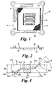
- a pin grid array in accordance with the present invention is shown and generally designated 10.
- the array 10 includes a base 12 which is substantially flat and which defines an upper surface 14 and a lower surface 16.
- the base 12 is made of a dielectric material, such as plastic.
- the pin grid array 10 of the present invention includes a plurality of electrical connectors 18 which are arranged on the base 12 to establish a matrix 20 of electrical contact points that extend outwardly from the upper surface 14. Similarly, the plurality of electrical connectors 18 also establish a matrix 22 of electrical contact points which extend outwardly from the lower surface 16. All of the connectors 18 are made of an electrically conducting material, such as a metal, and are oriented on the base 12 to establish a plurality of electrical circuit connections which pass from the upper surface 14 to the lower surface 16. With this arrangement, the matrix 20 and upper surface 14 of pin grid array 10 are engageable with an electronic device (not shown), while the matrix 22 and lower surface 16 of pin grid array 10 are engageable with another electronic device (also not shown).
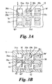
- the base 12 of pin grid array 10 is formed with a plurality of apertures 24, of which the apertures 24a-d are representative. These apertures 24 extend through the base 12 from first surface 14 to second surface 16 and are preferably arranged in rows and columns substantially as shown. Further, as perhaps best appreciated with reference to Figure 3B, each of the connectors 18 extend from the base 12 into two adjacent juxtaposed apertures 24. Specifically, consider the connector 18. Connector 18 includes two fingers 26a and 26b which have respective tips 28a and 28b. Further, the two fingers 26a and 26b are integral with a central portion 30 and extend from the central portion 30 into the respective apertures 24a and 24b. A more detailed appreciation of the cooperation between the base 12 and each individual connector 18 in the pin grid array 10 is possible with reference to Figure 4.
- each of the fingers 26a, 26b of connector 18 are bent at an angle ⁇ so that the respective tips 28a, 28b protrude from the apertures 24a, 24b.
- ⁇ is approximately equal to 45° and the tips 28a and 28b protrude outwardly from and beyond the respective surfaces 16, 14 of base 12. Specifically the tip 28a extends beyond the lower surface 16 through a deflection distance 32a, and the tip 28b extends beyond the upper surface 14 through a deflection distance 32b.
- the deflection distances 32a, 32b are preferably around 0.254 mm (ten thousandths of an inch (0.010 in.)).
- the connector 18 will have a configured length 34, as shown in Figure 4.
- the configured length 34 will be approximately 1.52 mm (sixty thousandths of an inch (0.060 in.)).
- the thickness 36 of base 12 from the upper surface 14 to the bottom surface 16 will be about 0.46 mm (eighteen thousandths of an inch (0.018 in.)).
- the plurality of the connectors 18 are stamped from a sheet 38 in a manner well known in the pertinent art. As intended for the present invention, all of the connectors 18 remain joined together at this stage of manufacture.
- the resultant pattern of connectors 18 which shows all of the connectors 18 joined together is, perhaps, best appreciated with reference to Figure 3B
- the stamped connectors 18 are initially joined together by tie bars 40 and, in turn, the tie bars 40 are appropriately joined together by cross bars 42.
- the fingers 26 of respective connectors 18 can also be formed with the angle ⁇ during this initial stamping.
- the angle ⁇ can be established subsequently, if desired.
- the tips 28 of the fingers 26 can be plated to enhance their electrical contact abilities. Preferably, this plating is done with gold, and is approximately 0.76 ⁇ m (thirty microns) thick.
- the stamped sheet 38 is then placed in the mold of an injection molding machine (not shown). Next, the base 12 is injection molded around portions of the sheet 38.
- the injection molding of base 12 onto and around portions of the stamped sheet 38 of connectors 18 is accomplished to achieve a certain orientation for the connectors 18 relative to the base 12. Specifically, the central portions 30 of all of the various connectors 18 are embedded into the base 12. This anchors the connectors 18 into the base 12. Additionally, as clearly shown by cross referencing Figures 3A, 3B and 4, the fingers 26 of all of the connectors 18 are cantilevered from the base 12 into juxtaposed apertures 24. For example, the fingers 26a, 26b of connector 18 are cantilevered in opposite directions into the juxtaposed apertures 24a, 24b. Further, their tips 28a, 28b extend beyond opposite surfaces 16, 14 of the base 12. Thus, an electrical circuit is established through the connector 18.
- an aperture 24 can accommodate two fingers 26, with each finger 26 being from a different connector 18.
- the finger 26b of connector 18 and the finger 26c of connector 18' are both cantilevered into the aperture 24b.
- the finger 26b of connector 18 extends beyond the upper surface 14 of base 12
- the finger 26c from the connector 18' will extend beyond the lower surface 16 of base 12.
- a similar arrangement of fingers 26 in apertures 24 thus continues in rows and columns throughout the pin grid array 10.
- the connectors 18 are electrically isolated from each other. This is done by a process generally referred to as "singulation". Specifically, the tie bars 40 (shown in Figure 3B) are removed. This can be done either mechanically or by any other means known in the art, such as by lasers. Access to the tie bars 40 for purpose of disconnecting the connectors 18 from each other is provided by the holes 44 (shown in Figure 3A) which are formed in the base 12 during the injection molding process. Singulation can be accomplished either while the base 12 is still in the mold, or after the combination of base 12 and connectors 18 is removed from the mold.
Landscapes
- Engineering & Computer Science (AREA)
- Microelectronics & Electronic Packaging (AREA)
- Coupling Device And Connection With Printed Circuit (AREA)
- Connecting Device With Holders (AREA)
Applications Claiming Priority (2)
| Application Number | Priority Date | Filing Date | Title |
|---|---|---|---|
| US08/937,101 US6045367A (en) | 1997-09-24 | 1997-09-24 | Multi-pin connector |
| US937101 | 1997-09-24 |
Publications (3)
| Publication Number | Publication Date |
|---|---|
| EP0906007A2 EP0906007A2 (en) | 1999-03-31 |
| EP0906007A3 EP0906007A3 (en) | 1999-09-29 |
| EP0906007B1 true EP0906007B1 (en) | 2003-04-09 |
Family
ID=25469509
Family Applications (1)
| Application Number | Title | Priority Date | Filing Date |
|---|---|---|---|
| EP98305772A Expired - Lifetime EP0906007B1 (en) | 1997-09-24 | 1998-07-20 | Multi-pin connector |
Country Status (5)
| Country | Link |
|---|---|
| US (2) | US6045367A (enExample) |
| EP (1) | EP0906007B1 (enExample) |
| JP (1) | JPH11126668A (enExample) |
| DE (2) | DE69813128T2 (enExample) |
| TW (1) | TW423186B (enExample) |
Cited By (1)
| Publication number | Priority date | Publication date | Assignee | Title |
|---|---|---|---|---|
| DE102016004520A1 (de) | 2016-04-13 | 2017-10-19 | Rosenberger Hochfrequenztechnik Gmbh & Co. Kg | Kontaktstift und Testsockel mit Kontaktstiften |
Families Citing this family (61)
| Publication number | Priority date | Publication date | Assignee | Title |
|---|---|---|---|---|
| US6293808B1 (en) * | 1999-09-30 | 2001-09-25 | Ngk Insulators, Ltd. | Contact sheet |
| JP2000168467A (ja) * | 1998-12-02 | 2000-06-20 | Yazaki Corp | 回路体への接続構造 |
| US6197171B1 (en) * | 1999-03-31 | 2001-03-06 | International Business Machines Corporation | Pin contact mechanism for plating pin grid arrays |
| US6193523B1 (en) * | 1999-04-29 | 2001-02-27 | Berg Technology, Inc. | Contact for electrical connector |
| JP4041619B2 (ja) * | 1999-05-28 | 2008-01-30 | 東京エレクトロン株式会社 | インターコネクタの製造方法 |
| JP3396807B2 (ja) * | 1999-06-25 | 2003-04-14 | 京セラエルコ株式会社 | 基板中継コネクタ |
| US6375474B1 (en) | 1999-08-09 | 2002-04-23 | Berg Technology, Inc. | Mezzanine style electrical connector |
| US6474997B1 (en) | 1999-09-30 | 2002-11-05 | Ngk Insulators, Ltd. | Contact sheet |
| EP1168510B1 (de) * | 2000-06-21 | 2004-09-01 | Itt Manufacturing Enterprises, Inc. | Elektrische Verbindungsvorrichtung |
| US6532654B2 (en) * | 2001-01-12 | 2003-03-18 | International Business Machines Corporation | Method of forming an electrical connector |
| JP2002231401A (ja) * | 2001-01-31 | 2002-08-16 | Molex Inc | ソケットコネクタ |
| US6604950B2 (en) | 2001-04-26 | 2003-08-12 | Teledyne Technologies Incorporated | Low pitch, high density connector |
| JP4667652B2 (ja) * | 2001-06-12 | 2011-04-13 | ローム株式会社 | 電池パック、およびその製造方法 |
| US6711026B2 (en) * | 2001-11-13 | 2004-03-23 | International Business Machines Corporation | Sash for land grid arrays |
| US6488513B1 (en) | 2001-12-13 | 2002-12-03 | Intercon Systems, Inc. | Interposer assembly for soldered electrical connections |
| US20040157476A1 (en) * | 2003-02-12 | 2004-08-12 | Ralph Maldonado | Perimeter sealed high density multi-pin connector |
| US6916181B2 (en) * | 2003-06-11 | 2005-07-12 | Neoconix, Inc. | Remountable connector for land grid array packages |
| US7758351B2 (en) | 2003-04-11 | 2010-07-20 | Neoconix, Inc. | Method and system for batch manufacturing of spring elements |
| US20050120553A1 (en) * | 2003-12-08 | 2005-06-09 | Brown Dirk D. | Method for forming MEMS grid array connector |
| US7244125B2 (en) | 2003-12-08 | 2007-07-17 | Neoconix, Inc. | Connector for making electrical contact at semiconductor scales |
| US7597561B2 (en) | 2003-04-11 | 2009-10-06 | Neoconix, Inc. | Method and system for batch forming spring elements in three dimensions |
| US7114961B2 (en) | 2003-04-11 | 2006-10-03 | Neoconix, Inc. | Electrical connector on a flexible carrier |
| US7113408B2 (en) | 2003-06-11 | 2006-09-26 | Neoconix, Inc. | Contact grid array formed on a printed circuit board |
| US20070020960A1 (en) | 2003-04-11 | 2007-01-25 | Williams John D | Contact grid array system |
| US7056131B1 (en) | 2003-04-11 | 2006-06-06 | Neoconix, Inc. | Contact grid array system |
| US7628617B2 (en) | 2003-06-11 | 2009-12-08 | Neoconix, Inc. | Structure and process for a contact grid array formed in a circuitized substrate |
| US8584353B2 (en) | 2003-04-11 | 2013-11-19 | Neoconix, Inc. | Method for fabricating a contact grid array |
| US7070419B2 (en) * | 2003-06-11 | 2006-07-04 | Neoconix Inc. | Land grid array connector including heterogeneous contact elements |
| US6869290B2 (en) * | 2003-06-11 | 2005-03-22 | Neoconix, Inc. | Circuitized connector for land grid array |
| US6994565B2 (en) * | 2003-07-14 | 2006-02-07 | Fci Americas Technology, Inc. | Electrical contact assembly with insulative carrier, stapled contact attachment and fusible element |
| TWM249244U (en) * | 2003-07-18 | 2004-11-01 | Hon Hai Prec Ind Co Ltd | Electrical connector |
| TWM250353U (en) * | 2003-08-06 | 2004-11-11 | Hon Hai Prec Ind Co Ltd | Electrical connector |
| US7185430B2 (en) * | 2003-11-28 | 2007-03-06 | Ngk Insulators, Ltd. | Method of manufacturing contact sheets |
| US6971885B2 (en) * | 2004-02-18 | 2005-12-06 | Teledyne Technologies Incorporated | Interconnect device with opposingly oriented contacts |
| TWI246799B (en) * | 2004-03-05 | 2006-01-01 | Hon Hai Prec Ind Co Ltd | Electrical connector |
| US7090503B2 (en) | 2004-03-19 | 2006-08-15 | Neoconix, Inc. | Interposer with compliant pins |
| US7025601B2 (en) | 2004-03-19 | 2006-04-11 | Neoconix, Inc. | Interposer and method for making same |
| WO2005091998A2 (en) | 2004-03-19 | 2005-10-06 | Neoconix, Inc. | Electrical connector in a flexible host |
| US7347698B2 (en) | 2004-03-19 | 2008-03-25 | Neoconix, Inc. | Deep drawn electrical contacts and method for making |
| US7695053B1 (en) * | 2004-04-16 | 2010-04-13 | Bae Systems Survivability Systems, Llc | Lethal threat protection system for a vehicle and method |
| US7354276B2 (en) | 2004-07-20 | 2008-04-08 | Neoconix, Inc. | Interposer with compliant pins |
| US20060141667A1 (en) * | 2004-12-23 | 2006-06-29 | Teradyne, Inc. | Bare die socket |
| WO2007043899A1 (en) | 2005-10-14 | 2007-04-19 | Applied Research Associates Nz Limited | A method of monitoring a surface feature and apparatus therefor |
| US7357644B2 (en) | 2005-12-12 | 2008-04-15 | Neoconix, Inc. | Connector having staggered contact architecture for enhanced working range |
| US7568917B1 (en) * | 2008-01-10 | 2009-08-04 | Tyco Electronics Corporation | Laminated electrical contact strip |
| US8212156B2 (en) * | 2008-06-26 | 2012-07-03 | International Business Machines Corporation | Plastic land grid array (PLGA) module and printed wiring board (PWB) with enhanced contact metallurgy construction |
| US7658617B1 (en) * | 2009-02-02 | 2010-02-09 | International Business Machines Corporation | Plastic land grid array (PLGA) module with inverted hybrid land grid array (LGA) interposer |
| JP5453016B2 (ja) * | 2009-08-18 | 2014-03-26 | 日本碍子株式会社 | フィルム状電気的接続体及びその製造方法 |
| US9179844B2 (en) | 2011-11-28 | 2015-11-10 | Aranz Healthcare Limited | Handheld skin measuring or monitoring device |
| US8641428B2 (en) | 2011-12-02 | 2014-02-04 | Neoconix, Inc. | Electrical connector and method of making it |
| JP6194580B2 (ja) * | 2012-12-03 | 2017-09-13 | 富士通株式会社 | ソケット及び電子部品搭載構造 |
| US9680273B2 (en) | 2013-03-15 | 2017-06-13 | Neoconix, Inc | Electrical connector with electrical contacts protected by a layer of compressible material and method of making it |
| CN104733976A (zh) * | 2013-12-23 | 2015-06-24 | 欣兴电子股份有限公司 | 连接器与其制作方法 |
| DE202014101769U1 (de) * | 2014-04-15 | 2015-07-17 | INTER CONTROL Hermann Köhler Elektrik GmbH & Co KG | Thermisches Schaltelement sowie Kontaktelement |
| US10013527B2 (en) | 2016-05-02 | 2018-07-03 | Aranz Healthcare Limited | Automatically assessing an anatomical surface feature and securely managing information related to the same |
| EP3497756B1 (en) * | 2016-08-11 | 2021-09-29 | D.M. Benatav Ltd. | Multiple diameter wire connection |
| US11116407B2 (en) | 2016-11-17 | 2021-09-14 | Aranz Healthcare Limited | Anatomical surface assessment methods, devices and systems |
| EP3606410B1 (en) | 2017-04-04 | 2022-11-02 | Aranz Healthcare Limited | Anatomical surface assessment methods, devices and systems |
| US12039726B2 (en) | 2019-05-20 | 2024-07-16 | Aranz Healthcare Limited | Automated or partially automated anatomical surface assessment methods, devices and systems |
| CN110718791B (zh) * | 2019-07-18 | 2021-05-28 | 得意精密电子(苏州)有限公司 | 电连接器 |
| CN113783066B (zh) * | 2021-08-09 | 2023-10-24 | 番禺得意精密电子工业有限公司 | 电连接器及其制造方法 |
Family Cites Families (15)
| Publication number | Priority date | Publication date | Assignee | Title |
|---|---|---|---|---|
| US4021091A (en) * | 1975-06-13 | 1977-05-03 | International Telephone And Telegraph Corporation | Zero force printed circuit board connector |
| US4159154A (en) * | 1978-04-10 | 1979-06-26 | International Telephone And Telegraph Corporation | Zero insertion force connector |
| JPS59132152A (ja) * | 1983-01-18 | 1984-07-30 | Japan Aviation Electronics Ind Ltd | セルフロツクコンタクト |
| JPH0638353B2 (ja) * | 1988-07-18 | 1994-05-18 | ヒロセ電機株式会社 | 電子部品用ソケット |
| US4867689A (en) * | 1988-10-31 | 1989-09-19 | Amp Incorporated | Elastomeric connector assembly |
| US4976629A (en) * | 1989-10-04 | 1990-12-11 | Teledyne Kinetics | Zero insertion force dual in-line LCD connector |
| US5147207A (en) * | 1990-10-30 | 1992-09-15 | Teledyne Kinetics | Balanced pressure connector |
| US5161982A (en) * | 1991-03-29 | 1992-11-10 | Teledyne Kinetics | Reactive base for cantilevered connector |
| EP0520080B2 (en) * | 1991-06-28 | 2005-03-30 | Molex Incorporated | IC card connector |
| US5139427A (en) * | 1991-09-23 | 1992-08-18 | Amp Incorporated | Planar array connector and flexible contact therefor |
| JPH06325810A (ja) * | 1993-03-08 | 1994-11-25 | Whitaker Corp:The | コンタクトモジュール及びそれを使用するピングリッドアレイ |
| US5395252A (en) * | 1993-10-27 | 1995-03-07 | Burndy Corporation | Area and edge array electrical connectors |
| US5462440A (en) * | 1994-03-11 | 1995-10-31 | Rothenberger; Richard E. | Micro-power connector |
| DE9407499U1 (de) * | 1994-05-05 | 1995-09-07 | Itt Composants Et Instruments, Dole Cedex | Elektrisches Kontaktelement |
| FR2737352B1 (fr) * | 1995-07-28 | 1997-08-29 | Itt Composants Instr | Connecteur electrique pour le raccordement d'une carte a circuit(s) integre(s) a contact |
-
1997
- 1997-09-24 US US08/937,101 patent/US6045367A/en not_active Expired - Fee Related
- 1997-11-24 US US08/977,414 patent/US5967797A/en not_active Expired - Lifetime
-
1998
- 1998-06-08 TW TW087109034A patent/TW423186B/zh not_active IP Right Cessation
- 1998-07-20 DE DE69813128T patent/DE69813128T2/de not_active Expired - Fee Related
- 1998-07-20 EP EP98305772A patent/EP0906007B1/en not_active Expired - Lifetime
- 1998-07-20 DE DE0906007T patent/DE906007T1/de active Pending
- 1998-08-07 JP JP10223508A patent/JPH11126668A/ja not_active Abandoned
Cited By (1)
| Publication number | Priority date | Publication date | Assignee | Title |
|---|---|---|---|---|
| DE102016004520A1 (de) | 2016-04-13 | 2017-10-19 | Rosenberger Hochfrequenztechnik Gmbh & Co. Kg | Kontaktstift und Testsockel mit Kontaktstiften |
Also Published As
| Publication number | Publication date |
|---|---|
| TW423186B (en) | 2001-02-21 |
| JPH11126668A (ja) | 1999-05-11 |
| DE69813128T2 (de) | 2003-12-24 |
| EP0906007A2 (en) | 1999-03-31 |
| EP0906007A3 (en) | 1999-09-29 |
| DE906007T1 (de) | 1999-09-16 |
| US5967797A (en) | 1999-10-19 |
| US6045367A (en) | 2000-04-04 |
| DE69813128D1 (de) | 2003-05-15 |
Similar Documents
| Publication | Publication Date | Title |
|---|---|---|
| EP0906007B1 (en) | Multi-pin connector | |
| KR100406598B1 (ko) | 전기커넥터및그제조방법 | |
| KR100464708B1 (ko) | 콘택트 시트 | |
| JP2819179B2 (ja) | 多接点電気コネクタ | |
| EP0838101B1 (en) | Electrical connectors | |
| JPH0371745B2 (enExample) | ||
| KR100669296B1 (ko) | 가압 접촉부를 갖는 전기 커넥터 | |
| US6830461B2 (en) | Electrical contact and electrical connection device using same | |
| EP0567006B1 (en) | Edge connector for a printed circuit board or the like | |
| KR100344050B1 (ko) | Pga 패키지용의 낮은 형상 전기 커넥터 및 단자 | |
| US6755683B2 (en) | Printed circuit connector | |
| KR20060113517A (ko) | 간단한 구조를 가지며 안정된 접속이 가능한 전기접속 부재및 그것을 사용하는 커넥터 | |
| JP2008226841A (ja) | 電気相互接続構造 | |
| EP1933426A1 (en) | Contact and electrical connector | |
| US5597320A (en) | Zero insertion force electrical connector and terminal | |
| JP3812937B2 (ja) | コネクタ | |
| EP0546673B1 (en) | Connector with retention feature | |
| KR100515993B1 (ko) | 전기 커넥터용 접촉자 및 그 접촉자를 구비한 전기커넥터 | |
| US6575791B1 (en) | Electrical connector providing reliable electrical interconnection with mated devices | |
| JP3252255B2 (ja) | Icソケット | |
| US7185430B2 (en) | Method of manufacturing contact sheets | |
| US7008241B2 (en) | Electrical connector assembly | |
| JP2022185269A (ja) | コネクタ | |
| JPH0329905Y2 (enExample) | ||
| JP3998209B2 (ja) | コネクタ |
Legal Events
| Date | Code | Title | Description |
|---|---|---|---|
| PUAI | Public reference made under article 153(3) epc to a published international application that has entered the european phase |
Free format text: ORIGINAL CODE: 0009012 |
|
| AK | Designated contracting states |
Kind code of ref document: A2 Designated state(s): DE FR GB |
|
| AX | Request for extension of the european patent |
Free format text: AL;LT;LV;MK;RO;SI |
|
| EL | Fr: translation of claims filed | ||
| RTI1 | Title (correction) |
Free format text: MULTI-PIN CONNECTOR |
|
| PUAL | Search report despatched |
Free format text: ORIGINAL CODE: 0009013 |
|
| DET | De: translation of patent claims | ||
| AK | Designated contracting states |
Kind code of ref document: A3 Designated state(s): AT BE CH CY DE DK ES FI FR GB GR IE IT LI LU MC NL PT SE |
|
| AX | Request for extension of the european patent |
Free format text: AL;LT;LV;MK;RO;SI |
|
| RIC1 | Information provided on ipc code assigned before grant |
Free format text: 6H 05K 7/10 A, 6H 01R 23/72 B, 6H 01R 13/24 B |
|
| 17P | Request for examination filed |
Effective date: 20000121 |
|
| AKX | Designation fees paid |
Free format text: DE FR GB |
|
| 17Q | First examination report despatched |
Effective date: 20020125 |
|
| GRAH | Despatch of communication of intention to grant a patent |
Free format text: ORIGINAL CODE: EPIDOS IGRA |
|
| GRAH | Despatch of communication of intention to grant a patent |
Free format text: ORIGINAL CODE: EPIDOS IGRA |
|
| GRAA | (expected) grant |
Free format text: ORIGINAL CODE: 0009210 |
|
| RIC1 | Information provided on ipc code assigned before grant |
Ipc: 7H 01R 13/24 B Ipc: 7H 01R 12/22 B Ipc: 7H 05K 7/10 A |
|
| AK | Designated contracting states |
Designated state(s): DE FR GB |
|
| REG | Reference to a national code |
Ref country code: GB Ref legal event code: FG4D |
|
| ET | Fr: translation filed | ||
| PLBE | No opposition filed within time limit |
Free format text: ORIGINAL CODE: 0009261 |
|
| STAA | Information on the status of an ep patent application or granted ep patent |
Free format text: STATUS: NO OPPOSITION FILED WITHIN TIME LIMIT |
|
| 26N | No opposition filed |
Effective date: 20040112 |
|
| PGFP | Annual fee paid to national office [announced via postgrant information from national office to epo] |
Ref country code: GB Payment date: 20040714 Year of fee payment: 7 |
|
| PGFP | Annual fee paid to national office [announced via postgrant information from national office to epo] |
Ref country code: FR Payment date: 20040720 Year of fee payment: 7 |
|
| PGFP | Annual fee paid to national office [announced via postgrant information from national office to epo] |
Ref country code: DE Payment date: 20040831 Year of fee payment: 7 |
|
| PG25 | Lapsed in a contracting state [announced via postgrant information from national office to epo] |
Ref country code: GB Free format text: LAPSE BECAUSE OF NON-PAYMENT OF DUE FEES Effective date: 20050720 |
|
| PG25 | Lapsed in a contracting state [announced via postgrant information from national office to epo] |
Ref country code: DE Free format text: LAPSE BECAUSE OF NON-PAYMENT OF DUE FEES Effective date: 20060201 |
|
| GBPC | Gb: european patent ceased through non-payment of renewal fee |
Effective date: 20050720 |
|
| PG25 | Lapsed in a contracting state [announced via postgrant information from national office to epo] |
Ref country code: FR Free format text: LAPSE BECAUSE OF NON-PAYMENT OF DUE FEES Effective date: 20060331 |
|
| REG | Reference to a national code |
Ref country code: FR Ref legal event code: ST Effective date: 20060331 |