EP0905856A1 - Verfahren und vorrichtung zur übertragung elektrischer energie - Google Patents
Verfahren und vorrichtung zur übertragung elektrischer energie Download PDFInfo
- Publication number
- EP0905856A1 EP0905856A1 EP98901104A EP98901104A EP0905856A1 EP 0905856 A1 EP0905856 A1 EP 0905856A1 EP 98901104 A EP98901104 A EP 98901104A EP 98901104 A EP98901104 A EP 98901104A EP 0905856 A1 EP0905856 A1 EP 0905856A1
- Authority
- EP
- European Patent Office
- Prior art keywords
- primary coil
- coil
- secondary coil
- current
- frequency
- Prior art date
- Legal status (The legal status is an assumption and is not a legal conclusion. Google has not performed a legal analysis and makes no representation as to the accuracy of the status listed.)
- Withdrawn
Links
Images


Classifications
-
- H—ELECTRICITY
- H02—GENERATION; CONVERSION OR DISTRIBUTION OF ELECTRIC POWER
- H02J—CIRCUIT ARRANGEMENTS OR SYSTEMS FOR SUPPLYING OR DISTRIBUTING ELECTRIC POWER; SYSTEMS FOR STORING ELECTRIC ENERGY
- H02J50/00—Circuit arrangements or systems for wireless supply or distribution of electric power
- H02J50/40—Circuit arrangements or systems for wireless supply or distribution of electric power using two or more transmitting or receiving devices
- H02J50/402—Circuit arrangements or systems for wireless supply or distribution of electric power using two or more transmitting or receiving devices the two or more transmitting or the two or more receiving devices being integrated in the same unit, e.g. power mats with several coils or antennas with several sub-antennas
-
- H—ELECTRICITY
- H02—GENERATION; CONVERSION OR DISTRIBUTION OF ELECTRIC POWER
- H02J—CIRCUIT ARRANGEMENTS OR SYSTEMS FOR SUPPLYING OR DISTRIBUTING ELECTRIC POWER; SYSTEMS FOR STORING ELECTRIC ENERGY
- H02J50/00—Circuit arrangements or systems for wireless supply or distribution of electric power
- H02J50/10—Circuit arrangements or systems for wireless supply or distribution of electric power using inductive coupling
- H02J50/12—Circuit arrangements or systems for wireless supply or distribution of electric power using inductive coupling of the resonant type
-
- H—ELECTRICITY
- H02—GENERATION; CONVERSION OR DISTRIBUTION OF ELECTRIC POWER
- H02J—CIRCUIT ARRANGEMENTS OR SYSTEMS FOR SUPPLYING OR DISTRIBUTING ELECTRIC POWER; SYSTEMS FOR STORING ELECTRIC ENERGY
- H02J50/00—Circuit arrangements or systems for wireless supply or distribution of electric power
- H02J50/90—Circuit arrangements or systems for wireless supply or distribution of electric power involving detection or optimisation of position, e.g. alignment
-
- H—ELECTRICITY
- H02—GENERATION; CONVERSION OR DISTRIBUTION OF ELECTRIC POWER
- H02J—CIRCUIT ARRANGEMENTS OR SYSTEMS FOR SUPPLYING OR DISTRIBUTING ELECTRIC POWER; SYSTEMS FOR STORING ELECTRIC ENERGY
- H02J2207/00—Indexing scheme relating to details of circuit arrangements for charging or depolarising batteries or for supplying loads from batteries
- H02J2207/20—Charging or discharging characterised by the power electronics converter
-
- H—ELECTRICITY
- H02—GENERATION; CONVERSION OR DISTRIBUTION OF ELECTRIC POWER
- H02J—CIRCUIT ARRANGEMENTS OR SYSTEMS FOR SUPPLYING OR DISTRIBUTING ELECTRIC POWER; SYSTEMS FOR STORING ELECTRIC ENERGY
- H02J50/00—Circuit arrangements or systems for wireless supply or distribution of electric power
- H02J50/70—Circuit arrangements or systems for wireless supply or distribution of electric power involving the reduction of electric, magnetic or electromagnetic leakage fields
-
- H—ELECTRICITY
- H02—GENERATION; CONVERSION OR DISTRIBUTION OF ELECTRIC POWER
- H02J—CIRCUIT ARRANGEMENTS OR SYSTEMS FOR SUPPLYING OR DISTRIBUTING ELECTRIC POWER; SYSTEMS FOR STORING ELECTRIC ENERGY
- H02J7/00—Circuit arrangements for charging or depolarising batteries or for supplying loads from batteries
- H02J7/007—Regulation of charging or discharging current or voltage
- H02J7/00712—Regulation of charging or discharging current or voltage the cycle being controlled or terminated in response to electric parameters
Definitions
- the present invention relates to an electric power transmission device and an electric power transmission method, and for example, is suitably applied to an electric power transmission device and an electric power transmission method to be used as a charger which charges electric power to a secondary battery built in a portable compact electronic equipment via a noncontact terminal.
- One type of the charger devices is a contact type.
- This contact type charger has such as a spring-loaded point of contact, and by contacting a point of contact of the portable compact electronic equipment side to the point of contact to electrically connect them, and the charging current is supplied to the secondary battery built in the portable compact electronic equipment via thus formed electric path.
- the point of contact may be oxidized or contaminants may be build up on the point of contact with time. These oxidation and contaminants cause the disconnection on the part of these contact points and hinder the supply of charging current to the secondary battery.
- a primary coil is provided on a terminal of the charger side and a secondary coil is provided on a terminal of the portable compact electronic equipment, and the primary coil and the secondary coil are brought close.
- the primary coil When an electric current is fed to the primary coil under this condition, the primary coil generates the magnetic flux.
- the current to be fed to the primary coil is turned ON or OFF at established intervals, the magnetic flux to be generated by the current induction varies with time.
- an inducted electromotive force is generated by the electromagnetic induction due to the linkage of the magnetic flux which varies with time.
- the primary coil generates alternating current of which the direction of current is reversed according to the ON/OFF of the primary coil side as inducted current with the inducted electromotive force as a power supply.
- the noncontact type charger conducts charging by supplying the inducted current to be generated in the secondary coil to the secondary battery as the charging current.
- the primary coil and the secondary coil are built in the charger side and the electronic equipment side respectively, and by transmitting the power by the electromagnetic induction from the primary coil to the secondary coil, the noncontact power transmission can be conducted.
- the present invention has been done considering the above point and is proposing an electric power transmission device and an electric power transmission method which are capable of improving the efficiency in electric power transmission from the primary coil side to the secondary coil side.
- the electric power transmission device for transmitting the electric power between the primary coil and the secondary coil, comprises signal generating means for generating and transmitting an oscillation signal formed of a fixed frequency, current supplying means for supplying the electric current to be conducted to the primary coil, driving means for drive-controlling the conduction and interception of the electric current to the primary coil based on the frequency of the oscillation signal, a primary coil for generating a magnetic flux which varies with time, based on the frequency of oscillation signal by drive controlling the conduction and interception of the electric current, and a secondary coil to which a capacitance element is connected in parallel, for generating an induced electromotive force according to the linkage of the magnetic flux which varies with time and is generated in the primary coil, and for performing resonant of the induced electric current to be generated between the capacitance element and the secondary coil based on the induced electromagnetic force with the frequency higher than the frequency of oscillation signal as the oscillation frequency, so that the inducted electromotive force can be transmitted
- the capacitance can be reduced and the coupling coefficient between the primary coil and the secondary coil can be apparently increased.
- the efficiency in the power transmission from the primary coil side to the secondary coil side can be improved.
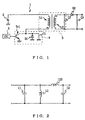
- numeral 1 generally shows a charger, in which a secondary battery is recharged by supplying the electric power sent out from a power source 2 to the secondary battery which is built in the prescribed electronic equipment via an electromagnetic induction section 3.
- the electromagnetic induction section 3 is comprised of a primary coil L1 placed in the charger 1 side and a secondary coil L2 provided in the electronic equipment, and these primary coil L1 and the secondary coil L2 do not have a point of contact with each other.
- One terminal of the primary coil L1 is connected to the power source 2, and both terminals of the secondary coil L2 are connected to the secondary battery.
- the charger 1 is comprised of the primary coil L1 and the secondary coil L2 which are winded around cores having the fixed shapes respectively and these cores are placed facing each other when charging.
- the other terminal of the primary coil L1 is connected to a driving circuit 4 and the driving circuit 4 is connected to a driving frequency generating unit 5.
- the driving frequency generating unit 5 generates an oscillation signal formed of the prescribed frequency f OSC and supplies this to the driving circuit 4.
- the driving circuit 4 feeds the supplied oscillation signal to a base electrode of a transistor Tr1 which is emitter grounded. When the voltage level of the oscillation signal entered into the base electrode is positive value, the transistor Tr1 conducts the current between the emitter electrode and the collector electrode. Thus, the current to be sent out from the power source 2 flows into the primary coil L1.
- the transistor Tr1 cuts off the conduction between the emitter electrode and the collector electrode.
- the current to be transmitted from the power source 2 does not flow into the primary coil L1, and an LC circuit formed by the primary coil L1 and a capacitor C1 of the driving circuit 4 forms a resonance circuit and an inverse electromotive force is generated in the primary coil L1.
- the current flows into the capacitor C1 to conduct the charging with the voltage by this inverse electromotive force as an electric source, and the current of the opposite direction flows into the primary coil L1 when the capacitor C1 conducts discharging to the primary coil L1.
- the current flowing into the primary coil L1 vibrates moving forward and backward alternately by the driving circuit 4, and accordingly, the voltage to be produced in the primary coil L1 becomes the form of horizontal pulse that changes based on the driving frequency f OSC to be transmitted from the driving frequency generating unit 5.
- the electronic equipment having the secondary coil L2 rectifies the induced current to be generated having the induced electromotive force as the power source, with the diode D2 and supplies this to the secondary battery to charge.
- the charger 1 transmits the electric power to be sent out from the power source 2 by the electromagnetic induction, from the primary coil L1 to the secondary coil L2 to charge.
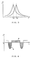
- Fig. 2 shows an equivalent circuit of the electromagnetic induction section 3 and LS2 shown in this Fig. is leakage inductance of the secondary coil L2 side.
- the resonant frequency f OUT is set to become higher than the frequency to drive-control the current flowing through the primary coil 1, that is the driving frequency f OSC .
- the resonant frequency f OUT with respect to the driving frequency f OSC can be set by adjusting the number of winds of the secondary coil L2 with respect to the number of winds of the primary coil or by adjusting the capacity of the resonant capacitor C2 connected to the secondary coil L2 in parallel.
- induction voltage formed of the resonant frequency f OUT is generated according to the temporal changes of magnetic flux generated in the primary coil L1.
- e 3 and e 4 show power elements based on the voltage and current, which is produced in the secondary coil L2.
- the power element e 3 corresponds to the power element e 1 and is produced in the secondary coil L2 when Tr1 is in the OFF condition.
- the power element e 4 corresponds to the power element e 2 and is produced in the secondary coil L2 when Tr1 is in the OFF condition.
- the power is taken by rectifying the induced current produced at the power element e 3 part, and supplied to the secondary battery.
- the transistor Tr1 of the driving circuit 4 becomes ON/OFF condition according to the frequency of the oscillation signal to be formed in the driving frequency generating unit 5, and when it is in the ON condition, the current to be supplied from the power source 2 flows through the primary coil L1. Moreover, when the transistor Tr1 is in the OFF condition, an inverse electromotive force is generated in the primary coil L1 and the capacitor C1 is charged. Thereafter, the capacitor C1 is discharged, thereby the current flows in the direction opposite to the time when the transistor Tr1 is in the ON condition. Thus, the magnetic flux produced in the primary coil L1 varies with time in accordance with the inversion of the current direction.
- An induced electromotive force is generated in the secondary coil L2 by the linkage of magnetic flux produced in the primary coil L1 and the direction of the induced electromotive force changes according to the temporal changes of magnetic flux.
- an induction voltage is generated by the resonant frequency f OUT with respect to the driving frequency f OSC by the inversion of the induced electromotive force.
- the current level becomes maximum when the voltage level is the largest since the current to be conducted into the primary coil L1 is in phase with the voltage due to the resonance.
- the secondary coil L2 side is resonated with such frequency, the power loss by the internal impedance on the LC circuit of the secondary coil L2 side becomes large and the efficiency in the power transmission cannot be improved.
- the induced current to be generated in the secondary coil L2 is formed of the alternating current as described above, and by decreasing the induced current while increasing the induction voltage, the power can be taken efficiently decreasing the power loss due to the internal impedance. Therefor, the induction voltage to be obtained in the secondary coil L2 side is required as high as possible.
- the part of power element e 3 at the time when the transistor Tr1 is in the OFF condition is rectified, thereby the power is taken from the induced current to be generated in the secondary coil L2 responding to the direction inversion of the current flowing through the primary coil L1.
- the power elements e 3 and e 4 areas of these elements are the same, and thus, the following relationship exists in these power elements; the width of the current T2 of the power element e 4 is narrower than the width of the current T1 of the power element e 3 , while the voltage value of the power element e 4 is larger than the voltage value of the power element e 3 .
- the electronic equipment having the secondary coil L2 rectifies the induced current of the power element e 3 part and takes out the power, the conduction angle of rectification can be made wider and a stable source power can be obtained.
- numeral 10 shows a charger having a source 2, an electromagnetic induction section 3, a driving circuit 4 and a driving frequency generating unit 5, similar to that of the battery device 1.
- the charger 10 has the primary coil L1 which is winded around a core having the fixed shape as the electromagnetic induction section 3 (Fig. 1), and when charging, the secondary coil L2 winded around a core arranged in the electronic equipment is placed at a position facing the core winded by the primary coil L1.
- the charger 10 drive-controls the conduction and interception to the primary coil L1 by turning the transistor Tr1 of the driving circuit 4 into the ON/OFF condition by the oscillation signal to be formed in the driving frequency generating unit 5 in order to flow the current through the primary coil L1 in the forward direction and the backward direction alternately.
- the time-varying magnetic flux is generated in the primary coil L1 by the current flowing in the forward direction and the backward direction, and an induced electromotive force is produced in the secondary coil L2 by the linkage of the magnetic flux, so that the resonant current flows by the LC resonance circuit formed of the secondary battery L2 and the capacitor C2 connected to the secondary coil L2 in parallel.
- the charger 10 is arranged in order that the resonant frequency of the secondary coil L2 becomes higher than the driving frequency of the primary coil L1 as in the case of the charger 1 (Fig. 3).
- the secondary coil L2 is formed by connecting two coils which are winded around in the same direction, while in the charger 1 in which the secondary coil L2 is formed with a single coil. More specifically, the charger 10 forms an electromagnetic induction section 3 by connecting coils L2A and L2B in series as the secondary coil L2, and after rectifying the voltage of the resonance circuit to be obtained by the inducted electromotive force generated according to the linkage of the magnetic flux, which is formed in the primary coil L1, toward the secondary coil L2, with diodes D2 and D3 respectively, supplies this into the secondary battery as a power source output.
- the voltage of the power element e 2A to be formed in the secondary coil L2A when the transistor Tr1 is in the OFF condition is smaller than the voltage of the power element e 2B to be formed in the secondary coil L2B when the transistor Tr1 is in the ON condition.
- the difference between these voltages becomes the variable value and unstable electric power. Accordingly, by adjusting the winding numbers of the secondary coil L2A and L2B, about equal values of voltage can be obtained in the secondary coil L2 side.
- the winding number of the secondary coil L2A is arranged to become larger than the winding number of the secondary coil L2B, and thus, the voltage values of resonant voltages to be obtained in the secondary coil L2A and L2B become approximately the same.
- the resonant frequency of the secondary coil L2A and the resonant frequency of the secondary coil L2B have phases shift each other by 180(° ), and the induced currents produced based on such resonant frequencies are rectified respectively by the diodes D2 and D3 and sent out.
- the ratio of the winding number of coil between the secondary coil L2A and L2B is adjusted so that the winding number of coil of the secondary coil L2A is larger than the winding number of coil of the secondary coil L2B and the induction voltage to be generated in the secondary coil L2A and the induction voltage to be generated in the secondary coil L2B become approximately the same values.
- the induced current of the power element e 2A formed in the secondary coil L2A and the induced current of the power element e 2B formed in the secondary coil L2B according to the time-varying of magnetic flux of the primary coil L1 can be taken out as the electric power, and the electric power can be taken out in either case where the transistor Tr1 is in the ON or OFF condition.
- the resonant frequency to be formed in the secondary coil L2 side is arranged so as to become higher than the driving frequency of the primary coil L1
- the secondary coils L2A and L2B having about equal values of induction voltages which can be obtained by adjusting the winding number of the secondary coil L2A becomes larger than the winding number of the secondary coil L2B are connected and placed in the electronic equipment and the resonant voltages to be formed respectively are rectified and sent out.
- the apparent coupling coefficient can be increased by increasing the efficiency factor Q and at the same time, the resonant voltages of the power elements e 2A and e 2B to be produced in the secondary coils L2A and L2B can be taken out as the source power.
- the efficiency in power transmission from the primary coil L1 to the secondary coil L2 can be improved and the stable power can be obtained regardless of the current direction of the primary coil L1.
- numeral 20 shows a charger comprised of a power source 2, an electromagnetic induction section 3, a driving circuit 4 and a driving frequency generating unit 5 which have the same construction as the charger 1.
- the charging unit 20 has the primary coil L1 winded around a core of the fixed shape as the electromagnetic induction section 3 (Fig. 1), and when charging, the core winded by the secondary coil L2 provided in the electronic equipment is placed on the position facing the core winded by the primary coil L1.
- the charger 20 drive-controls the conduction and interception to the primary coil L1 by turning the transistor Tr1 of the driving circuit 4 ON or OFF by the oscillation signal generated in the driving frequency generating unit 5 in order to supply the current to the primary coil L1 in the forward direction and the backward direction alternately.
- the time-varying magnetic flux is generated in the primary coil L1 by the current flowing in the forward direction and the backward direction, and an induced electromotive force is formed in the secondary coil L2 by the linkage of the magnetic flux, and resonant current flows by the LC circuit of the secondary coil L2 and the capacitor C2 connected in parallel to the secondary coil L2.
- the charger 20 is so arranged that the resonant frequency of the secondary coil L2 becomes higher than the driving frequency of the primary coil L1 as in the case of charger 1.
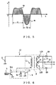
- the charger 20 is different from the charger 1 on the loading condition of the primary coil L1 and the secondary coil L2 and sizes of cores winded by the coils.
- the cross sectional area of the core winded by the secondary coil L2 is smaller than the cross sectional area of the core winded by the primary coil L1, and when charging, the core winded by the primary coil L1 and the core winded by the secondary coil L2 are placed, in which their centers shift each other.
- the core of the primary coil L1 side has the fixed ring shape and a part of the core is cut off at the fixed position on the ring and separated by the fixed distance.
- the core winded by the secondary coil L2 is inserted between the opposite cross sections spaced and is placed facing each cross section.
- the charger 20 places the secondary coil L2 in order that the center of the core winded by the secondary coil L2 is shifted from the center of the core winded by the primary coil L1 in the desired direction.
- the charger 20 by locating the position of the outer region of the core winded by the secondary coil L2 onto the position of one of the outer regions of the core winded by the primary coil L1, the core of the secondary coil L2 side is placed on the position shifted from the center of the core of the primary coil side.
- the resonant frequency of the secondary coil L2 is set to become higher than the driving frequency of the primary coil L1 according to such arrangements.
- the core winded by the secondary coil L2 is inserted between the cross sections separated of the core winded by the primary coil L1 and its center of the core is placed on the position shifted from the center of the core of the primary coil L1 side.
- the resonant frequency is set to become higher than the driving frequency of the primary coil L1 side on the position.
- the magnetic flux is generated between the cross sections of each core of the primary coil L1 side, which are separated by the fixed distance, by the current flowing through the primary coil L1, and the driving circuit 4 reverses the direction of current flowing through the primary coil L1 based on the frequency of the oscillation signal to be transmitted from the driving frequency generating unit 5 in order to change the magnetic flux to be produced in the primary coil L1 over time.
- the induced electromotive force which reverses in accordance with the time-varying magnetic flux is generated in the secondary coil L2, and the induced current can be obtained with the induced electromotive force as an electric source.
- magnetic energy of the magnetic flux causes linkage between the other parts stored in the electronic equipment having the secondary coil L2 and affects these parts and there are cases where heat is generated or operation errors occur.
- the core winded by the secondary coil L2 is placed on the position at least separate from the center of the core of the primary coil L1, the effect of magnetic flux to the other electronic parts in the electronic equipment equipped with the secondary coil L2 is and thereby the generation of heat caused by the magnetic field and operation errors can be prevented.
- the cross sectional area of the core of the secondary coil L2 side is made smaller than the cross sectional area of the core of the primary coil L1 side, if the cores are placed on positions shifted each other, scattering of the magnetic field to be formed between the primary coil L1 and the secondary coil L2 can be decreased. Furthermore, since the cross sectional area of the core is made smaller, a storage capacity of the secondary coil core in the electronic equipment having the secondary coil L2 can be made smaller, thus, the electronic equipment can be minimized.
- numeral 30 shows a charger comprised of a source 2, an electromagnetic induction section 3 and a driving circuit 4 as the similar construction to the charger 1.
- the charger 30 is comprised of the primary coil L1 which winds around the core having the fixed shape as an electromagnetic induction section 3, and when charging, the core winded by the secondary coil L2 placed in the electronic equipment is placed at the position facing the core winded by the primary coil L1.
- the charger 30 turns the transistor Tr1 of the driving circuit 4 ON/OFF by an oscillation signal generated in the driving frequency generating unit 5 to drive-control the conduction and interception to the primary coil L1 and flows the current to the primary coil L1 in the forward direction and the backward direction alternately.
- a time-varying magnetic flux is generated in the primary coil L1 and an induced electromotive force is produced by the linkage of the magnetic flux and resonant current flows and resonance occurs by the LC circuit.
- the charger 30 is arranged so that the resonant frequency of the secondary coil L2 becomes higher than the driving frequency of the primary coil L1 as in the case with the charger 1 (Fig. 3).
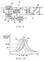
- the charger 30 is constructed differently from the charger 1 with the added devices, comprising a variable frequency generating unit 31 capable of varying the frequency of oscillation signal to be generated in place of the driving frequency generating unit 5 (Fig. 1), a voltage detection unit 32, a oscillation frequency control unit 33, and an input voltage control unit 34.
- the charger 30 controls the variable frequency generating unit 31 by the oscillation frequency control unit 33 depending on the detection result of the voltage by the voltage detection unit 32 and simultaneously controls an input voltage to be supplied from the power source 2 by the input voltage control unit 34.
- the frequency and input voltage of the oscillation signal varies.
- the variable frequency generating unit 31 supplies the generated oscillation signal to the driving circuit 4.
- the driving circuit drive-controls the current to be conducted to the primary coil L1 in accordance with the voltage level of the oscillation signal to flow the current in the forward direction and the backward direction alternately. Accordingly, the magnetic flux generated in the primary coil L1 varies with time.
- the secondary coil L2 generates an induced electromotive force in accordance with the linkage of the magnetic flux to be generated in the primary coil L1 and obtains an induced current which reverse according to the time-change of the magnetic flux with the induced electromotive force as the power source.
- an output voltage V of the secondary coil L2 side drops due to the load.
- Such output voltage drop affects the primary coil L1 side causing drop in the voltage to be generated in the primary coil L1.
- the charger 30 detects such voltage drops caused by the load, by the voltage detection unit 32 connected to the primary coil L1 in parallel.
- the charger 30 also detects the voltage rise by the voltage detection unit 32.
- the reference voltage is set in advance in the voltage detection unit 32 and at the time when the drop or rise of the voltage is detected, a detection signal S1 is sent to the oscillation frequency control unit 33 and the input voltage control unit 34.
- the oscillation frequency control unit 33 supplies a control signal S2 to the variable frequency generating unit 31 in accordance with the detection signal S1, and when the voltage drop is detected, rises the frequency of oscillation signal formed by the variable frequency generating unit 31, and when the voltage rise is detected, drops the frequency of the oscillation signal formed by the variable frequency generating unit 31. Furthermore, the input voltage control unit 34 controls the input voltage supplied from the power source 2, in accordance with the detection signal S1, and when the voltage drop is detected, the input voltage control unit 34, after rising the input voltage, sends it out to the primary coil L1, and when the voltage rise is detected, after dropping the input voltage, sends it out to the primary coil L1.
- the value of the induction voltage to be generated in the secondary coil L2 side is set to become the maximum value at the time when the resonant frequency f OUT , i.e., the induced current produces resonance.
- the charger 30 adjusts the driving frequency f OSC within the fixed frequency range under the resonance frequency f OUT of the secondary coil L2 side by the variable frequency generating unit 31.
- the driving frequency varies within the variable range by the variable frequency generating unit 31, and by changing the resonance frequency in the primary coil L1 side, the induction voltage to be generated in the secondary coil L2 side is risen or dropped.
- the induction voltage V 2 to be generated in the secondary coil L2 can be risen by ⁇ V 2 .
- the charger 30 detects the drop of the induction voltage indirectly by the voltage detection unit 32, and as a result of this detection, controlling the variable frequency generating unit 31 by the oscillation frequency control unit 33, rises the frequency of the oscillation signal, and simultaneously rises the power source voltage to be supplied from the power source 2 by the input voltage control unit 34 and supplying it to the primary coil L1.
- the induction voltage can be increased by the voltage value dropped and the fixed voltage can be maintained as shown by a broken line in Fig.
- the fixed voltage is maintained.
- the charger 30 performs maintenance of the induction voltage to be generated in the secondary coil L2 side according to the procedure shown in Fig. 12. More specifically, firstly the charger 30 starts the procedure at step SP1. After starting the procedure, at step SP2, the charger 30 detects the voltage changes occurred in the primary coil L1 by the voltage detection unit 32. The charger 30 judges the detection result by using the detection signal S1. If the voltage drop is recognized at step SP3, it proceeds to step SP5. In addition, if the voltage drop is not recognized as the detection result by the detection signal S1, it proceeds to step SP4. The charger 30 judges the detection result by using the detection signal S1 and if the voltage rise is recognized at step SP4, proceeds to step SP6. Moreover, if the voltage rise is not recognized as the detection result by the detection signal S1, returns to step SP2.
- the charger 30 raises the frequency f 1 of the oscillation signal by ⁇ f 1 , at step SP5, according to the control of the variable frequency generating unit 31 by the oscillation frequency control unit 33, and raises the input voltage V 1 by ⁇ V 1 according to the control of the input voltage by the input voltage control unit 34. Moreover, if the voltage rise is recognized at step SP4, the charger 30, at step SP6, lowers the frequency f 1 of the oscillation signal by ⁇ f 1 according to the control of the variable frequency generating unit 31 by the oscillation frequency control unit 33, and also lowers the input voltage V 1 by ⁇ V 1 according to the control of the input voltage by the input voltage control unit 34.
- the charger 30 After conducting the frequency control and input voltage control, the charger 30 returns to step SP2 and repeats the procedure till the voltage drop or rise are not detected by the voltage detection, and by controlling the driving frequency and input voltage, compensates for the amount of voltage drop or rise of the induction voltage in the secondary coil L2 side.
- the charger 30 detects the voltage changes occurred in the primary coil L1 by the voltage detection unit 32.
- the charger 30 informs the detection result to the oscillation frequency control unit 33 and the input voltage control unit 34 by using the detection signal S1.
- the oscillation frequency control unit 33 controls the variable frequency generating unit 31 in accordance with the information and raises the frequency of the oscillation signal.
- the input voltage control unit 34 after controlling and increasing the power source voltage to be supplied from the power source 2, transmits it to the primary coil L1.
- the charger 30 can increase the induction voltage of the secondary coil L2 side indirectly by controlling the frequency and the input voltage of the oscillation signal. And if the induction voltage drops by connecting the load in the secondary coil L2 side, the charger 30 can increase the induction voltage by controlling the driving frequency and the input voltage, and maintain the induction voltage at the constant level to make it stable. When the voltage rises, the charger 30 can decrease the induction voltage in the same manner and thus, can maintain the induction voltage at the constant level to make it stable.
- the charger 30 is arranged to increase or decrease the voltage by the control of the input voltage by the input voltage control unit 34 as well as the control of the driving frequency by the oscillation frequency control unit 33.
- the induction voltage can be corrected accurately by using the frequency control at the same time.
- the construction of the charger 40 differs from that of the charger 30 in that a driving circuit 41 for flowing the current periodically to the primary coil L1 in accordance with the frequency of the oscillation signal is provided in place of the driving circuit 4 which flows the current to the primary coil L1 in the forward and backward directions in accordance with the frequency of the oscillation signal, a damper diode D4 is connected to the primary coil L1 by another coil, and a pulse width control unit 42 is provided between the variable frequency generating unit 31 and the driving circuit 41 as well as eliminating the voltage control unit 34 (Fig. 9).
- the present invention can be utilized for a charger which conducts charging to the secondary battery built in a portable compact electronic equipment.
Landscapes
- Engineering & Computer Science (AREA)
- Computer Networks & Wireless Communication (AREA)
- Power Engineering (AREA)
- Charge And Discharge Circuits For Batteries Or The Like (AREA)
Applications Claiming Priority (3)
| Application Number | Priority Date | Filing Date | Title |
|---|---|---|---|
| JP20739/97 | 1997-02-03 | ||
| JP2073997 | 1997-02-03 | ||
| PCT/JP1998/000441 WO1998034319A1 (fr) | 1997-02-03 | 1998-02-03 | Equipement et procede pour le transfert d'energie electrique |
Publications (2)
| Publication Number | Publication Date |
|---|---|
| EP0905856A1 true EP0905856A1 (de) | 1999-03-31 |
| EP0905856A4 EP0905856A4 (de) | 2001-04-04 |
Family
ID=12035575
Family Applications (1)
| Application Number | Title | Priority Date | Filing Date |
|---|---|---|---|
| EP98901104A Withdrawn EP0905856A4 (de) | 1997-02-03 | 1998-02-03 | Verfahren und vorrichtung zur übertragung elektrischer energie |
Country Status (6)
| Country | Link |
|---|---|
| EP (1) | EP0905856A4 (de) |
| JP (1) | JP3692541B2 (de) |
| CN (1) | CN1105414C (de) |
| AU (1) | AU732701B2 (de) |
| TW (1) | TW493312B (de) |
| WO (1) | WO1998034319A1 (de) |
Cited By (6)
| Publication number | Priority date | Publication date | Assignee | Title |
|---|---|---|---|---|
| GB2347801A (en) * | 1999-03-10 | 2000-09-13 | Ea Tech Ltd | Electric vehicle battery charger |
| US7554316B2 (en) | 2004-05-11 | 2009-06-30 | Access Business Group International Llc | Controlling inductive power transfer systems |
| EP2317627B1 (de) * | 2009-10-28 | 2016-07-13 | TDK Corporation | Drahtlose Leistungszufuhr, drahtloses Leistungsübertragungssystem und Tisch und Tischlampe damit |
| US9450455B2 (en) | 2009-12-16 | 2016-09-20 | Fujitsu Limited | Magnetic resonance power transmitter and magnetic resonance power receiver |
| EP3352330A4 (de) * | 2015-09-17 | 2019-05-29 | IHI Corporation | Stromübertragungsvorrichtung und kontaktloses stromversorgungssystem |
| US10985616B2 (en) | 2018-03-30 | 2021-04-20 | STMicroelectronics (Grand Ouest) SAS | Contactless transmitter |
Families Citing this family (31)
| Publication number | Priority date | Publication date | Assignee | Title |
|---|---|---|---|---|
| US7212414B2 (en) | 1999-06-21 | 2007-05-01 | Access Business Group International, Llc | Adaptive inductive power supply |
| CN1813396B (zh) * | 2003-05-23 | 2010-04-28 | 奥克兰联合服务有限公司 | 谐振变换器及其方法以及感耦电能传送系统 |
| AU2004241915A1 (en) * | 2003-05-23 | 2004-12-02 | Auckland Uniservices Limited | Methods and apparatus for control of inductively coupled power transfer systems |
| JP4156537B2 (ja) * | 2004-01-21 | 2008-09-24 | 理想科学工業株式会社 | 給電装置 |
| JP2005210800A (ja) * | 2004-01-21 | 2005-08-04 | Riso Kagaku Corp | 給電装置 |
| US7310245B2 (en) | 2005-04-22 | 2007-12-18 | Noboru Ohbo | Electric power transmission device and electric power transmission method |
| US9774086B2 (en) | 2007-03-02 | 2017-09-26 | Qualcomm Incorporated | Wireless power apparatus and methods |
| CN100576711C (zh) * | 2007-03-29 | 2009-12-30 | 雅米科技股份有限公司 | 感应电力系统 |
| JP2010193598A (ja) * | 2009-02-17 | 2010-09-02 | Nippon Soken Inc | 非接触給電設備および非接触給電システム |
| JP4815499B2 (ja) * | 2009-02-27 | 2011-11-16 | 東光株式会社 | 非接触電力伝送回路 |
| JP5362453B2 (ja) * | 2009-06-16 | 2013-12-11 | 三洋電機株式会社 | 充電台 |
| JPWO2011064879A1 (ja) * | 2009-11-27 | 2013-04-11 | 富士通株式会社 | 送電装置および電力伝送装置 |
| JP2011177009A (ja) * | 2010-01-26 | 2011-09-08 | Equos Research Co Ltd | 非接触送電システム |
| BR112012019690A2 (pt) * | 2010-02-10 | 2016-05-03 | Fujitsu Ltd | método de controle de frequência ressonante, dispositivo transmissor de energia elétrica, dispositivo receptor de energia elétrica em sistema de transmissão de energia do tipo de acoplamento ressonante magnético |
| EP2536002A4 (de) | 2010-02-10 | 2017-03-29 | Fujitsu Limited | Resonanzfrequenzsteuerungsverfahren, leistungsübertragungsvorrichtung und leistungsempfangsvorrichtung für ein leistungsübertragungssystem mit magnetresonanzkopplung |
| JP2011167036A (ja) | 2010-02-15 | 2011-08-25 | Toyota Industries Corp | 車両用給電装置および受電装置 |
| JP5516149B2 (ja) * | 2010-06-30 | 2014-06-11 | ソニー株式会社 | 端末装置更新方法及び端末装置 |
| US9088307B2 (en) * | 2010-12-29 | 2015-07-21 | National Semiconductor Corporation | Non-resonant and quasi-resonant system for wireless power transmission to multiple receivers |
| KR101813129B1 (ko) | 2011-05-04 | 2017-12-28 | 삼성전자주식회사 | 무선 전력 송수신 시스템 |
| JP5988191B2 (ja) * | 2011-09-27 | 2016-09-07 | 株式会社エクォス・リサーチ | 電力伝送システム |
| KR101802441B1 (ko) * | 2011-11-17 | 2017-11-29 | 삼성전자주식회사 | 무선 에너지 수신 장치, 무선 에너지 송신 장치, 이를 포함하는 무선 에너지 전송 시스템 및 무선 에너지 전송 방법 |
| WO2013080860A1 (ja) * | 2011-11-28 | 2013-06-06 | 株式会社 豊田自動織機 | 非接触給電装置 |
| JP2013115909A (ja) * | 2011-11-28 | 2013-06-10 | Toyota Industries Corp | 非接触給電装置 |
| JP2013211932A (ja) * | 2012-03-30 | 2013-10-10 | Equos Research Co Ltd | 電力伝送システム |
| JP2014030288A (ja) * | 2012-07-31 | 2014-02-13 | Sony Corp | 給電装置および給電システム |
| JP6379660B2 (ja) * | 2013-06-27 | 2018-08-29 | Tdk株式会社 | ワイヤレス受電装置、及び、ワイヤレス電力伝送装置 |
| US10283995B2 (en) * | 2014-02-28 | 2019-05-07 | L'oreal | Charge current monitoring or control in a resonance-tuned inductive charger |
| WO2016163092A1 (ja) * | 2015-04-06 | 2016-10-13 | パナソニックIpマネジメント株式会社 | 非接触給電装置 |
| JP6737648B2 (ja) * | 2016-06-30 | 2020-08-12 | パナソニック株式会社 | 送電装置 |
| JP2018113831A (ja) * | 2017-01-13 | 2018-07-19 | オムロン株式会社 | 非接触給電装置 |
| JP7102944B2 (ja) * | 2018-05-29 | 2022-07-20 | オムロン株式会社 | 非接触給電装置 |
Citations (3)
| Publication number | Priority date | Publication date | Assignee | Title |
|---|---|---|---|---|
| US4831507A (en) * | 1988-09-12 | 1989-05-16 | Reliance Comm/Tec Corporation | Frequency controlled preload |
| EP0580107A1 (de) * | 1992-07-20 | 1994-01-26 | Daifuku Co., Ltd. | Magnetschwebetransportsystem |
| EP0653831A1 (de) * | 1993-11-15 | 1995-05-17 | Kabushiki Kaisha Toshiba | Leistungsschaltung |
Family Cites Families (9)
| Publication number | Priority date | Publication date | Assignee | Title |
|---|---|---|---|---|
| US4001665A (en) * | 1975-04-21 | 1977-01-04 | Burroughs Corporation | High efficiency power supply having a reactive buck automatic d.c. voltage regulator |
| US4331225A (en) * | 1978-04-25 | 1982-05-25 | Bolger John G | Power control system for electrically driven vehicle |
| US4654880A (en) * | 1983-12-09 | 1987-03-31 | Minnesota Mining And Manufacturing Company | Signal transmission system |
| AU5481786A (en) * | 1985-03-20 | 1986-09-25 | Hochmair, E.S. | Transcutaneous power and signal transmission system |
| US4679560A (en) * | 1985-04-02 | 1987-07-14 | Board Of Trustees Of The Leland Stanford Junior University | Wide band inductive transdermal power and data link |
| US4802080A (en) * | 1988-03-18 | 1989-01-31 | American Telephone And Telegraph Company, At&T Information Systems | Power transfer circuit including a sympathetic resonator |
| US5095224A (en) * | 1990-08-31 | 1992-03-10 | Siemens-Pacesetter, Inc. | Interrupted resonance energy transfer system |
| JP2803943B2 (ja) * | 1992-10-21 | 1998-09-24 | アルプス電気株式会社 | 非接触電力供給装置 |
| JP3761001B2 (ja) * | 1995-11-20 | 2006-03-29 | ソニー株式会社 | 非接触型情報カード及びic |
-
1998
- 1998-02-03 JP JP53272798A patent/JP3692541B2/ja not_active Expired - Fee Related
- 1998-02-03 TW TW087101315A patent/TW493312B/zh not_active IP Right Cessation
- 1998-02-03 CN CN98800344A patent/CN1105414C/zh not_active Expired - Fee Related
- 1998-02-03 WO PCT/JP1998/000441 patent/WO1998034319A1/ja not_active Application Discontinuation
- 1998-02-03 AU AU56805/98A patent/AU732701B2/en not_active Ceased
- 1998-02-03 EP EP98901104A patent/EP0905856A4/de not_active Withdrawn
Patent Citations (3)
| Publication number | Priority date | Publication date | Assignee | Title |
|---|---|---|---|---|
| US4831507A (en) * | 1988-09-12 | 1989-05-16 | Reliance Comm/Tec Corporation | Frequency controlled preload |
| EP0580107A1 (de) * | 1992-07-20 | 1994-01-26 | Daifuku Co., Ltd. | Magnetschwebetransportsystem |
| EP0653831A1 (de) * | 1993-11-15 | 1995-05-17 | Kabushiki Kaisha Toshiba | Leistungsschaltung |
Non-Patent Citations (1)
| Title |
|---|
| See also references of WO9834319A1 * |
Cited By (14)
| Publication number | Priority date | Publication date | Assignee | Title |
|---|---|---|---|---|
| GB2347801B (en) * | 1999-03-10 | 2001-01-17 | Ea Tech Ltd | Battery chargers |
| GB2347801A (en) * | 1999-03-10 | 2000-09-13 | Ea Tech Ltd | Electric vehicle battery charger |
| US9544022B2 (en) | 2004-05-11 | 2017-01-10 | Access Business Group International Llc | Controlling inductive power transfer systems |
| US7554316B2 (en) | 2004-05-11 | 2009-06-30 | Access Business Group International Llc | Controlling inductive power transfer systems |
| US7868587B2 (en) | 2004-05-11 | 2011-01-11 | Access Business Group International Llc | Controlling inductive power transfer systems |
| US8035340B2 (en) | 2004-05-11 | 2011-10-11 | Access Business Group International Llc | Controlling inductive power transfer systems |
| US8610400B2 (en) | 2004-05-11 | 2013-12-17 | Access Business Group International Llc | Controlling inductive power transfer systems |
| US10673281B2 (en) | 2004-05-11 | 2020-06-02 | Philips Ip Ventures B.V. | Controlling inductive power transfer systems |
| EP2317627B1 (de) * | 2009-10-28 | 2016-07-13 | TDK Corporation | Drahtlose Leistungszufuhr, drahtloses Leistungsübertragungssystem und Tisch und Tischlampe damit |
| US9450455B2 (en) | 2009-12-16 | 2016-09-20 | Fujitsu Limited | Magnetic resonance power transmitter and magnetic resonance power receiver |
| EP3352330A4 (de) * | 2015-09-17 | 2019-05-29 | IHI Corporation | Stromübertragungsvorrichtung und kontaktloses stromversorgungssystem |
| US10714942B2 (en) | 2015-09-17 | 2020-07-14 | Ihi Corporation | Power transmitter and wireless power transfer system |
| EP4243240A3 (de) * | 2015-09-17 | 2024-01-03 | IHI Corporation | Stromübertragungsvorrichtung und kontaktloses stromversorgungssystem |
| US10985616B2 (en) | 2018-03-30 | 2021-04-20 | STMicroelectronics (Grand Ouest) SAS | Contactless transmitter |
Also Published As
| Publication number | Publication date |
|---|---|
| TW493312B (en) | 2002-07-01 |
| CN1105414C (zh) | 2003-04-09 |
| AU5680598A (en) | 1998-08-25 |
| AU732701B2 (en) | 2001-04-26 |
| EP0905856A4 (de) | 2001-04-04 |
| JP3692541B2 (ja) | 2005-09-07 |
| WO1998034319A1 (fr) | 1998-08-06 |
| CN1220781A (zh) | 1999-06-23 |
Similar Documents
| Publication | Publication Date | Title |
|---|---|---|
| US5991170A (en) | Equipment and method for transmitting electric power | |
| AU732701B2 (en) | Electric power transmission device and electric power transmission method | |
| US10892648B2 (en) | Wireless power transfer method, apparatus and system for low and medium power | |
| EP2211438B1 (de) | Kontaktfreies Leistungsübertragungssystem | |
| US10336201B2 (en) | Contactless power transmission system | |
| JP6077563B2 (ja) | ワイヤレス電力システム及び方法 | |
| JP2803943B2 (ja) | 非接触電力供給装置 | |
| EP2824799B1 (de) | Energieübertragungssystem | |
| US9831681B2 (en) | Power reception apparatus and power receiving method | |
| US9774218B2 (en) | Non-contact power feeding apparatus | |
| CN111082533B (zh) | 控制装置、输电装置、电力传输系统、受电装置和设备 | |
| US10938244B2 (en) | Bidirectional wireless power transmission system | |
| JP2012070463A (ja) | 非接触給電装置 | |
| CN115152125A (zh) | 具有调谐调整电路的无线功率馈送系统 | |
| EP0954089A2 (de) | Getakteter Resonanzwandler | |
| US10447091B2 (en) | Power transmission unit of wireless power feeding device | |
| WO2020203690A1 (ja) | 受電装置、移動体、および無線電力伝送システム | |
| CA2250244C (en) | Equipment and method for transmitting electric power | |
| JPWO2020049853A1 (ja) | 非接触給電システム | |
| JP6685016B2 (ja) | 非接触給電装置、プログラム、非接触給電装置の制御方法、及び非接触電力伝送システム | |
| US20240234003A9 (en) | Contactless power feed apparatus and power transmission coil | |
| US20230187982A1 (en) | Contactless power feeding apparatus | |
| JP2021083140A (ja) | 受電装置 | |
| WO2024062758A1 (ja) | 給電装置 | |
| JP7117219B2 (ja) | 無線給電装置およびこれを用いた多軸ロボット |
Legal Events
| Date | Code | Title | Description |
|---|---|---|---|
| PUAI | Public reference made under article 153(3) epc to a published international application that has entered the european phase |
Free format text: ORIGINAL CODE: 0009012 |
|
| 17P | Request for examination filed |
Effective date: 19980910 |
|
| AK | Designated contracting states |
Kind code of ref document: A1 Designated state(s): DE FR GB |
|
| A4 | Supplementary search report drawn up and despatched |
Effective date: 20010216 |
|
| AK | Designated contracting states |
Kind code of ref document: A4 Designated state(s): DE FR GB |
|
| RIC1 | Information provided on ipc code assigned before grant |
Free format text: 7H 02J 17/00 A, 7H 02J 5/00 B, 7H 02M 3/335 B, 7H 02J 7/02 B |
|
| STAA | Information on the status of an ep patent application or granted ep patent |
Free format text: STATUS: THE APPLICATION HAS BEEN WITHDRAWN |
|
| 18W | Application withdrawn |
Withdrawal date: 20020925 |