EP0904923A1 - Verfahren und System zum Formen - Google Patents
Verfahren und System zum Formen Download PDFInfo
- Publication number
- EP0904923A1 EP0904923A1 EP98307890A EP98307890A EP0904923A1 EP 0904923 A1 EP0904923 A1 EP 0904923A1 EP 98307890 A EP98307890 A EP 98307890A EP 98307890 A EP98307890 A EP 98307890A EP 0904923 A1 EP0904923 A1 EP 0904923A1
- Authority
- EP
- European Patent Office
- Prior art keywords
- molding material
- mold
- mold cavity
- wave energy
- molding
- Prior art date
- Legal status (The legal status is an assumption and is not a legal conclusion. Google has not performed a legal analysis and makes no representation as to the accuracy of the status listed.)
- Withdrawn
Links
Images

Classifications
-
- B—PERFORMING OPERATIONS; TRANSPORTING
- B29—WORKING OF PLASTICS; WORKING OF SUBSTANCES IN A PLASTIC STATE IN GENERAL
- B29C—SHAPING OR JOINING OF PLASTICS; SHAPING OF MATERIAL IN A PLASTIC STATE, NOT OTHERWISE PROVIDED FOR; AFTER-TREATMENT OF THE SHAPED PRODUCTS, e.g. REPAIRING
- B29C35/00—Heating, cooling or curing, e.g. crosslinking or vulcanising; Apparatus therefor
- B29C35/02—Heating or curing, e.g. crosslinking or vulcanizing during moulding, e.g. in a mould
- B29C35/0261—Heating or curing, e.g. crosslinking or vulcanizing during moulding, e.g. in a mould using ultrasonic or sonic vibrations
-
- B—PERFORMING OPERATIONS; TRANSPORTING
- B29—WORKING OF PLASTICS; WORKING OF SUBSTANCES IN A PLASTIC STATE IN GENERAL
- B29C—SHAPING OR JOINING OF PLASTICS; SHAPING OF MATERIAL IN A PLASTIC STATE, NOT OTHERWISE PROVIDED FOR; AFTER-TREATMENT OF THE SHAPED PRODUCTS, e.g. REPAIRING
- B29C45/00—Injection moulding, i.e. forcing the required volume of moulding material through a nozzle into a closed mould; Apparatus therefor
- B29C45/17—Component parts, details or accessories; Auxiliary operations
- B29C45/46—Means for plasticising or homogenising the moulding material or forcing it into the mould
- B29C45/56—Means for plasticising or homogenising the moulding material or forcing it into the mould using mould parts movable during or after injection, e.g. injection-compression moulding
- B29C45/568—Applying vibrations to the mould parts
-
- B—PERFORMING OPERATIONS; TRANSPORTING
- B29—WORKING OF PLASTICS; WORKING OF SUBSTANCES IN A PLASTIC STATE IN GENERAL
- B29C—SHAPING OR JOINING OF PLASTICS; SHAPING OF MATERIAL IN A PLASTIC STATE, NOT OTHERWISE PROVIDED FOR; AFTER-TREATMENT OF THE SHAPED PRODUCTS, e.g. REPAIRING
- B29C45/00—Injection moulding, i.e. forcing the required volume of moulding material through a nozzle into a closed mould; Apparatus therefor
- B29C45/02—Transfer moulding, i.e. transferring the required volume of moulding material by a plunger from a "shot" cavity into a mould cavity
-
- B—PERFORMING OPERATIONS; TRANSPORTING
- B29—WORKING OF PLASTICS; WORKING OF SUBSTANCES IN A PLASTIC STATE IN GENERAL
- B29C—SHAPING OR JOINING OF PLASTICS; SHAPING OF MATERIAL IN A PLASTIC STATE, NOT OTHERWISE PROVIDED FOR; AFTER-TREATMENT OF THE SHAPED PRODUCTS, e.g. REPAIRING
- B29C45/00—Injection moulding, i.e. forcing the required volume of moulding material through a nozzle into a closed mould; Apparatus therefor
- B29C45/14—Injection moulding, i.e. forcing the required volume of moulding material through a nozzle into a closed mould; Apparatus therefor incorporating preformed parts or layers, e.g. injection moulding around inserts or for coating articles
- B29C45/14819—Injection moulding, i.e. forcing the required volume of moulding material through a nozzle into a closed mould; Apparatus therefor incorporating preformed parts or layers, e.g. injection moulding around inserts or for coating articles the inserts being completely encapsulated
-
- B—PERFORMING OPERATIONS; TRANSPORTING
- B29—WORKING OF PLASTICS; WORKING OF SUBSTANCES IN A PLASTIC STATE IN GENERAL
- B29C—SHAPING OR JOINING OF PLASTICS; SHAPING OF MATERIAL IN A PLASTIC STATE, NOT OTHERWISE PROVIDED FOR; AFTER-TREATMENT OF THE SHAPED PRODUCTS, e.g. REPAIRING
- B29C45/00—Injection moulding, i.e. forcing the required volume of moulding material through a nozzle into a closed mould; Apparatus therefor
- B29C45/17—Component parts, details or accessories; Auxiliary operations
- B29C45/46—Means for plasticising or homogenising the moulding material or forcing it into the mould
- B29C45/58—Details
- B29C45/585—Vibration means for the injection unit or parts thereof
-
- H10W74/016—
-
- B—PERFORMING OPERATIONS; TRANSPORTING
- B29—WORKING OF PLASTICS; WORKING OF SUBSTANCES IN A PLASTIC STATE IN GENERAL
- B29C—SHAPING OR JOINING OF PLASTICS; SHAPING OF MATERIAL IN A PLASTIC STATE, NOT OTHERWISE PROVIDED FOR; AFTER-TREATMENT OF THE SHAPED PRODUCTS, e.g. REPAIRING
- B29C45/00—Injection moulding, i.e. forcing the required volume of moulding material through a nozzle into a closed mould; Apparatus therefor
- B29C45/17—Component parts, details or accessories; Auxiliary operations
- B29C45/46—Means for plasticising or homogenising the moulding material or forcing it into the mould
- B29C45/56—Means for plasticising or homogenising the moulding material or forcing it into the mould using mould parts movable during or after injection, e.g. injection-compression moulding
- B29C45/568—Applying vibrations to the mould parts
- B29C2045/5685—Applying vibrations to the mould parts for eliminating internal voids in the moulding material
Definitions
- This invention relates generally to the molding of plastics and more particularly to the application of vibration waves during the process of molding plastics or other materials.
- Plastics, or polymers are used in a variety of products and applications ranging from the simple pen to the complicated wing of an aircraft. Different types of plastics, or polymers, as they are technically known, generally have different mechanical, chemical, and electrical properties that allow plastics to be used in many applications. Plastics are typically formed into a product through a molding process, such as transfer molding, injection molding, sheet molding, or blow molding.
- plastics are used extensively in the computer and semiconductor industry in a wide variety of applications.
- One such application is the encapsulation of semiconductor devices, particularly integrated circuits. Encapsulating a semiconductor device in plastic materials protects the device from environmental damage and also provides structural strength to the semiconductor device.
- Internal voids often degrade mechanical, electrical, and chemical properties of the semiconductor device, as well as the appearance of the molded product.
- internal voids reduce the reliability of the package because they allow moisture to accumulate within the voids. This moisture may cause corrosion of the semiconductor device and may promote cracking when the encapsulated semiconductor device is subjected to a vapor phase reflow or a similar process.
- a molding system and method is disclosed herein that addresses shortcomings of prior molding systems and processes.
- a method for molding includes forming a mold containing at least one mold cavity. Molding material is transferred into each mold cavity, and wave energy is applied to the molding material contained within each mold cavity to impede the formation of internal voids within the molding material.
- a transfer system is connected to the mold cavity through a runner system. The transfer system operates to transfer non-solidified molding material into the mold cavity. The non-solidified molding material contained within the mold cavity encapsulates the semiconductor device.
- a frequency system applies vibration waves to the non-solidified molding material disposed within the mold cavity.
- the invention provides several technical advantages. For example, the invention improves the quality of the finished molded product by reducing or eliminating internal voids, at least in part, breaking up large bubbles formed by the clustering or grouping of small bubbles. The invention also prevents the formation of large bubbles caused by back pressure and flow stoppage at the completion of cavity filling and allows an even dispersion of small voids, which do not result in internal voids.
- the invention allows the density of the molded product, or package density, to be increased. The increase in package density allows the encapsulation of a next generation of semiconductor devices that have an ever increasing number of leads.
- FIGURES 1 through 5 of the drawings in which like numerals refer to like parts throughout the several views.
- the invention relates to the formation of internal voids in a solidified molding material or package. It has been determined that internal voids are formed by the grouping or clustering of small air bubbles and voids when a mold cavity is filling with non-solidified molding material. The non-solidified molding material then solidifies or hardens with internal voids in the solidified molding material or package. The grouping of small bubbles into larger sizes, thereby forming internal voids, is often caused by back pressure when the flow of non-solidified molding material into the mold cavity stops at the completion of mold cavity filling. In addition, the formation of small bubbles when the non-solidified molding material is flowing is inherent to the molding process. Small bubbles are formed as the molding material begins to flow to the mold cavity. Wave energy is applied to the molding material contained within the mold cavity to reduce or eliminate small bubbles and voids that may group or cluster to form internal voids.
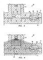
- FIGURE 1 is a schematic cross section in part of one embodiment of a mold system 20, and FIGURE 2 is a cross section of mold system 20 taken along line 2-2 of FIGURE 1.
- Mold system 20 may include a mold 21 having a mold cavity 28, a transfer system 25 to transfer mold material 60 into mold cavity 28, and a frequency system 70 to apply wave energy 72, as illustrated in FIGURE 4, to mold material 60 within mold cavity 28.
- Mold 21 may include a first chase 30 and a second chase 32, which cooperate to form a system of passages and cavities between the chases.
- mold cavity 28 is connected to a pot 22 by a runner system 24.
- Runner system 24 includes gate 26, which forms the transition of runner system 24 to mold cavity 28.
- Mold 21 is a multipot mold; however, the teachings may be applied to other mold designs, including single pot molds, pencil molds, and gauged pot molds.
- pot 22 is shown as part of first chase 30, pot 22 may also be formed as part of second chase 32.
- pot 22 stores molding material 60 for use in mold system 20. Pot 22 may be formed in any shape or size suitable for molding applications.
- a plunger 31 corresponding to the shape and size of pot 22 may be slidably disposed within pot 22 to apply a compressive load to molding material 60 contained within pot 22.
- Molding material 60 is disposed within pot 22 between plunger 31 and runner system 24.
- FIGURE 1 illustrates plunger 31 in a non-compressive load position, in which plunger 31 is not applying a compressive load to molding material 60 contained within pot 22.
- Molding material 60 may be any type of plastic or polymer, such as thermosets or thermoplastics. Prior to the molding process, molding material 60 may be in the form of powder, granules, cold compacted powder, or a liquid. Powder and granule molding materials 60 may contain 30-50% of entrained air. Cold compacted powder molding materials 60 may contain 10-20% of entrained air, whereas liquid molding materials 60 contain much less entrained air 62.
- a lead frame 52 may be loaded between first chase 30 and second chase 32.
- Lead frame 52 may include multiple semiconductor devices 50.
- mold cavity 28 is formed around semiconductor device 50.
- transfer system 25 may be any device or system operable to transfer non-solidified mold material 60 into mold cavity 28.
- Transfer system 25 may include plunger 31 in cooperation with pot 22 and runner system 24 that communicates non-solidified molding material 60 from pot 22 to mold cavity 28.
- FIGURES 3 and 4 are schematic cross sections in part of one embodiment of a mold system 20 during the molding process.
- FIGURE 3 illustrates mold system 20 during transfer of molding material 60 from pot 22 to mold cavity 28, which is commonly referred to in the art as the transfer phase.
- FIGURE 4 illustrates mold system 20 after transfer of molding material 60 into mold cavity 28, during compression of molding material 60 and during the application of wave energy 72 to molding material 60. Compression of molding material 60 is commonly referred to in the art as the packing phase.
- Frequency system 70 is operable to apply wave energy 72 to molding material 60 contained within mold cavity 28.
- frequency system 70 may include a high frequency horn that is directly or indirectly attached to plunger 31; a transducer that is connected to plunger 31; or a servo-valve connected to a hydraulic system that provides the compressive load to plunger 31; however, frequency system 70 may include other transducers and techniques for applying wave energy 72 to molding material 60 contained within mold cavity 28.
- Wave energy may be energy of any suitable wave type, frequency, and intensity that reduces or prevents the formation of internal voids.
- wave energy 72 may be vibration waves greater than 1,000 cycles per second; however, ultrasonic waves, which are waves greater than 20 kHz, have been found to be particularly effective in reducing internal voids 62.
- Vibration waves may include both longitudinal waves, which are alternating waves of rarefaction and compression, and transverse waves, which are shear waves perpendicular to the direction of compressive wave propagation.
- wave energy 72 may be varied depending upon the application.
- wave energy 72 may be a square wave wherein the intensity of wave energy 72 is constant, a ramping wave wherein the intensity of wave energy 72 ramps from low to high or vice versa, or a sinusoidal wave wherein the intensity of wave energy 72 varies according to a sinusoidal wave.
- a wave energy 72 intensity greater than 20 kHz is preferable; however, a wave energy 72 intensity of 5 kHz, 10 kHz, and 15 kHz may be used with the present invention.
- wave energy 72 may have a frequency that matches, or is a multiple of, a natural frequency of molding material 60 or mold cavity 28.
- the natural frequency of mold material 60 is defined herein to be that frequency or frequency range that best implodes entrained air or bubbles 62 in mold material 60, thereby preventing internal voids in the molded package. Because mold material 60 may contain different fillers, different mold materials 60 may have different natural frequencies.
- the natural frequency of mold cavity 28 is defined herein to include those frequencies or frequency ranges that amplify wave energy 72 within mold cavity 28.
- the duration of wave energy 72 may also be varied. Wave energy 72 may be applied continuously, in pulses, or a combination of continuous and pulse. Continuous application of wave energy 72, as used herein, is the application of wave energy 72 during the molding process for a single discrete time period. The continuous application of wave energy 72 may include varying the intensity of wave energy 72 during the continuous application of wave energy 72.
- the pulse application of wave energy 72 as used herein, is the application of wave energy 72 during discrete time periods with discrete time periods between each pulse that wave energy 72 is not applied. The intensity of wave energy 72 during each pulse of wave energy 72 may be varied.
- Wave energy 72 may be applied at any time during the molding process.
- wave energy 72 may be applied during the transfer phase at a constant intensity to reduce the formation of bubbles 62 and to help transfer molding material 60 from pot 22 to mold cavity 28 through runner system 24.
- Wave energy 72, with the pulses having a different intensity, may then be applied during the packing phase to break up and implode bubbles 62 that cause internal voids in molding material 60 within mold cavity 28.
- molding material 60 is placed within pot 22 between plunger 31 and runner system 24, as illustrated in FIGURE 1.
- Pot 22 may contain a heating element to melt molding material 60.
- mold 20 may contain a heating element to elevate the temperature of mold 21 to accelerate the molding process.
- plunger 31 extends toward runner system 24, thereby applying a compressive load to non-solidified molding material 60 contained within pot 22.
- non-solidified molding material 60 flows through runner system 24 and gate 26 into mold cavity 28.
- a flow front 64 is formed at the leading edge of non-solidified molding material 60 as it flows through the runner system 24 and into mold cavity 28.
- Flow front 64 captures air during the transfer phase and is characterized by a frothy appearance.
- non-solidified molding material 60 essentially fills mold cavity 60
- the momentum of molding material 60 can cause back pressure in mold cavity 28, which disrupts the flow of non-solidified molding material 60 and causes additional bubbles 62 to be formed in mold material 60.
- the entrained air or bubbles 62 are preferably eliminated or reduced in size to avoid internal voids.
- plunger 31 extends farther toward runner system 24, increasing the compressive load on non-solidified molding material 60 contained within pot 22.
- the increased pressure is communicated through runner system 24 to mold cavity 28, thereby increasing the compressive pressure on non-solidified molding material 60 within mold cavity 28.
- packing is not always a necessity, its purpose is to help reduce the entrained air or bubbles 62 that cause internal voids by compressing air bubbles 62.
- wave energy 72 may be applied at the packing phase of the molding process. Wave energy 72 implodes or breaks up bubbles 62 that may cause internal voids. Wave energy 72 also increases the package density of solidified molding material 60 by vibrating or pulsating non-solidified molding material 60 into the minute details of mold cavity 28. Non-solidified molding material 60 is then allowed to solidify or harden, for example, by cooling, at which time first chase 30 and second chase 32 of mold 21 may be separated to allow the removal of the encapsulated semiconductor device or package.
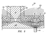
- FIGURE 5 is a schematic cross section in part of a mold system 120.
- Mold system 120 is analogous to mold system 20, except that frequency system 170, which is analogous to frequency system 70, is associated with a mold 121.
- the operation of mold system 120 as shown in FIGURE 5 is analogous to mold system 20, described above.
- the invention provides an efficient and effective method and system for reducing or eliminating air bubbles or voids that may cause internal voids in a final molded product.
- the present invention increases the quality of the final molded product.
Landscapes
- Engineering & Computer Science (AREA)
- Manufacturing & Machinery (AREA)
- Mechanical Engineering (AREA)
- Physics & Mathematics (AREA)
- Health & Medical Sciences (AREA)
- Oral & Maxillofacial Surgery (AREA)
- Thermal Sciences (AREA)
- Moulds For Moulding Plastics Or The Like (AREA)
- Injection Moulding Of Plastics Or The Like (AREA)
- Encapsulation Of And Coatings For Semiconductor Or Solid State Devices (AREA)
Applications Claiming Priority (2)
| Application Number | Priority Date | Filing Date | Title |
|---|---|---|---|
| US6056097P | 1997-09-30 | 1997-09-30 | |
| US60560P | 1997-09-30 |
Publications (1)
| Publication Number | Publication Date |
|---|---|
| EP0904923A1 true EP0904923A1 (de) | 1999-03-31 |
Family
ID=22030286
Family Applications (1)
| Application Number | Title | Priority Date | Filing Date |
|---|---|---|---|
| EP98307890A Withdrawn EP0904923A1 (de) | 1997-09-30 | 1998-09-29 | Verfahren und System zum Formen |
Country Status (5)
| Country | Link |
|---|---|
| EP (1) | EP0904923A1 (de) |
| JP (1) | JPH11170298A (de) |
| KR (1) | KR19990030273A (de) |
| SG (1) | SG89265A1 (de) |
| TW (1) | TW436405B (de) |
Cited By (8)
| Publication number | Priority date | Publication date | Assignee | Title |
|---|---|---|---|---|
| EP1621315A4 (de) * | 2003-04-25 | 2007-08-29 | Hoya Corp | Formverfahren und formvorrichtung, das bzw. die ultraschallschwingungen verwendet und optische linse |
| EP2266776A1 (de) * | 2009-06-27 | 2010-12-29 | Bayer MaterialScience AG | Verfahren und Vorrichtung zur Herstellung von dickwandigen Kunststoff-Bauteilen, insbesondere optischen Bauteilen |
| DE102014008603A1 (de) | 2013-06-21 | 2014-12-24 | Engel Austria Gmbh | Mischkopf mit auf Mischkammer gerichteten Wellenemitter |
| CN107718464A (zh) * | 2017-09-29 | 2018-02-23 | 中南大学 | 一种超声塑化成型系统及成型方法 |
| CN107718465A (zh) * | 2017-09-29 | 2018-02-23 | 中南大学 | 一种超声塑化微注射成型的装置及成型方法 |
| CN110275242A (zh) * | 2018-03-16 | 2019-09-24 | 洛克威尔柯林斯公司 | 柔性光导和照明系统 |
| DE102023001020A1 (de) * | 2022-09-19 | 2024-03-21 | Eleadtk Co., Ltd. | Verfahren zum ausbilden einer schutzschicht auf einem elektronischen modul |
| WO2025058626A1 (en) * | 2023-09-14 | 2025-03-20 | W. L. Gore & Associates, Inc. | Processing of protein using ultrasonic vibration energy |
Families Citing this family (1)
| Publication number | Priority date | Publication date | Assignee | Title |
|---|---|---|---|---|
| KR102736568B1 (ko) * | 2019-12-27 | 2024-12-03 | 삼성전자주식회사 | 반도체 패키지 제조방법 |
Citations (7)
| Publication number | Priority date | Publication date | Assignee | Title |
|---|---|---|---|---|
| JPS5434762A (en) * | 1977-08-24 | 1979-03-14 | Hitachi Ltd | Resin-sealing metal mold |
| JPS60244512A (ja) * | 1984-05-21 | 1985-12-04 | Hitachi Ltd | 成形方法 |
| DE3516666A1 (de) * | 1985-05-09 | 1986-11-13 | Heinz Dr.-Ing. 5100 Aachen Derek | Verfahren zur erzeugung eines formteils, insbesondere aus niedrigviskosen formmassen |
| JPH04273132A (ja) * | 1991-02-27 | 1992-09-29 | Mitsubishi Electric Corp | 半導体装置の樹脂封止方法 |
| JPH05326598A (ja) * | 1992-05-20 | 1993-12-10 | Toowa Kk | 電子部品の樹脂封止成形方法 |
| JPH06262639A (ja) * | 1993-03-15 | 1994-09-20 | Nippo Sangyo Kk | 合成樹脂の成形方法及び成形装置 |
| JPH09312308A (ja) * | 1996-05-21 | 1997-12-02 | Oki Electric Ind Co Ltd | 半導体装置の製造方法及びその製造装置 |
Family Cites Families (1)
| Publication number | Priority date | Publication date | Assignee | Title |
|---|---|---|---|---|
| JPH05273132A (ja) * | 1992-03-25 | 1993-10-22 | Fuji Electric Co Ltd | セラミックスの組成分析方法 |
-
1998
- 1998-09-08 SG SG9803581A patent/SG89265A1/en unknown
- 1998-09-28 TW TW087116029A patent/TW436405B/zh not_active IP Right Cessation
- 1998-09-29 EP EP98307890A patent/EP0904923A1/de not_active Withdrawn
- 1998-09-29 KR KR1019980040646A patent/KR19990030273A/ko not_active Withdrawn
- 1998-09-30 JP JP10278516A patent/JPH11170298A/ja active Pending
Patent Citations (7)
| Publication number | Priority date | Publication date | Assignee | Title |
|---|---|---|---|---|
| JPS5434762A (en) * | 1977-08-24 | 1979-03-14 | Hitachi Ltd | Resin-sealing metal mold |
| JPS60244512A (ja) * | 1984-05-21 | 1985-12-04 | Hitachi Ltd | 成形方法 |
| DE3516666A1 (de) * | 1985-05-09 | 1986-11-13 | Heinz Dr.-Ing. 5100 Aachen Derek | Verfahren zur erzeugung eines formteils, insbesondere aus niedrigviskosen formmassen |
| JPH04273132A (ja) * | 1991-02-27 | 1992-09-29 | Mitsubishi Electric Corp | 半導体装置の樹脂封止方法 |
| JPH05326598A (ja) * | 1992-05-20 | 1993-12-10 | Toowa Kk | 電子部品の樹脂封止成形方法 |
| JPH06262639A (ja) * | 1993-03-15 | 1994-09-20 | Nippo Sangyo Kk | 合成樹脂の成形方法及び成形装置 |
| JPH09312308A (ja) * | 1996-05-21 | 1997-12-02 | Oki Electric Ind Co Ltd | 半導体装置の製造方法及びその製造装置 |
Non-Patent Citations (6)
| Title |
|---|
| PATENT ABSTRACTS OF JAPAN vol. 10, no. 115 (M - 474) 30 April 1986 (1986-04-30) * |
| PATENT ABSTRACTS OF JAPAN vol. 17, no. 69 (E - 1318) 10 February 1993 (1993-02-10) * |
| PATENT ABSTRACTS OF JAPAN vol. 18, no. 141 (E - 1520) 9 March 1994 (1994-03-09) * |
| PATENT ABSTRACTS OF JAPAN vol. 18, no. 666 (M - 1724) 15 December 1994 (1994-12-15) * |
| PATENT ABSTRACTS OF JAPAN vol. 3, no. 56 (E - 110) 15 May 1979 (1979-05-15) * |
| PATENT ABSTRACTS OF JAPAN vol. 98, no. 4 31 March 1998 (1998-03-31) * |
Cited By (15)
| Publication number | Priority date | Publication date | Assignee | Title |
|---|---|---|---|---|
| EP1621315A4 (de) * | 2003-04-25 | 2007-08-29 | Hoya Corp | Formverfahren und formvorrichtung, das bzw. die ultraschallschwingungen verwendet und optische linse |
| EP2266776A1 (de) * | 2009-06-27 | 2010-12-29 | Bayer MaterialScience AG | Verfahren und Vorrichtung zur Herstellung von dickwandigen Kunststoff-Bauteilen, insbesondere optischen Bauteilen |
| DE102014008603A1 (de) | 2013-06-21 | 2014-12-24 | Engel Austria Gmbh | Mischkopf mit auf Mischkammer gerichteten Wellenemitter |
| AT514610B1 (de) * | 2013-06-21 | 2015-02-15 | Engel Austria Gmbh | Mischkopf mit auf Mischkammer gerichteten Wellenemitter |
| AT514610A4 (de) * | 2013-06-21 | 2015-02-15 | Engel Austria Gmbh | Mischkopf mit auf Mischkammer gerichteten Wellenemitter |
| CN107718465A (zh) * | 2017-09-29 | 2018-02-23 | 中南大学 | 一种超声塑化微注射成型的装置及成型方法 |
| CN107718464A (zh) * | 2017-09-29 | 2018-02-23 | 中南大学 | 一种超声塑化成型系统及成型方法 |
| CN107718464B (zh) * | 2017-09-29 | 2019-07-30 | 中南大学 | 一种超声塑化成型系统及成型方法 |
| CN110275242A (zh) * | 2018-03-16 | 2019-09-24 | 洛克威尔柯林斯公司 | 柔性光导和照明系统 |
| EP3540301A3 (de) * | 2018-03-16 | 2020-02-26 | Rockwell Collins, Inc. | Flexibler lichtleiter und beleuchtungssystem |
| US10684406B2 (en) | 2018-03-16 | 2020-06-16 | Rockwell Collins, Inc. | Flexible light guide and lighting system |
| DE102023001020A1 (de) * | 2022-09-19 | 2024-03-21 | Eleadtk Co., Ltd. | Verfahren zum ausbilden einer schutzschicht auf einem elektronischen modul |
| US12150249B2 (en) | 2022-09-19 | 2024-11-19 | Eleadtk Co., Ltd. | Method for forming a protective film on an electronic module |
| DE102023001020B4 (de) * | 2022-09-19 | 2025-10-02 | Eleadtk Co., Ltd. | Verfahren zum ausbilden einer schutzschicht auf einem elektronischen modul |
| WO2025058626A1 (en) * | 2023-09-14 | 2025-03-20 | W. L. Gore & Associates, Inc. | Processing of protein using ultrasonic vibration energy |
Also Published As
| Publication number | Publication date |
|---|---|
| TW436405B (en) | 2001-05-28 |
| KR19990030273A (ko) | 1999-04-26 |
| JPH11170298A (ja) | 1999-06-29 |
| SG89265A1 (en) | 2002-06-18 |
Similar Documents
| Publication | Publication Date | Title |
|---|---|---|
| EP0904923A1 (de) | Verfahren und System zum Formen | |
| JP4991335B2 (ja) | 材料を押圧するための工程及び装置 | |
| US5431854A (en) | Method for pressing a plastic, which cures by means of a reaction, into a mould cavity, a pressing auxiliary in pill form to be used in this method and a holder composed of such material | |
| JPH04147814A (ja) | 樹脂封入成形用金型 | |
| EP1114709A4 (de) | Gerät und verfahren zum schaumformen von kunstharz in internen formen und dadurch hergestelltes erzeugnis | |
| CA2355642A1 (en) | Method and apparatus for blow molding large reinforced plastic parts | |
| EP1060507B1 (de) | Formteil, form und herstellungsverfahren zum umhüllen von elektronischen bauteilen auf einem träger | |
| KR100682179B1 (ko) | 수지 성형용 형 및 수지 성형 방법 | |
| EP1074367A3 (de) | Vorrichtung und Verfahren zum Formgiessen von Epoxy-Harzartikeln | |
| CA2189304A1 (en) | Process for Producing a Bumper for a Vehicle | |
| US6214273B1 (en) | Molding method with the use of modified runners | |
| CN207682806U (zh) | 一种半导体封装模具及封装装置 | |
| WO2004009273A3 (de) | Umformung eines kristallisierbaren materials im flüssigen oder pastösen zustand | |
| JPS60244512A (ja) | 成形方法 | |
| JPS57142328A (en) | Method for injection blow molding | |
| JP3022419B2 (ja) | 半導体樹脂封止金型 | |
| JPS6056520A (ja) | トランスフア−モ−ルド装置 | |
| EP0681897A1 (de) | Vorrichtung und Verfahren zur Versiegelung mit Harz | |
| JPH01182016A (ja) | プラスチック射出成形方法 | |
| JP3453476B2 (ja) | 射出成形方法および射出成形装置 | |
| JP2003100786A (ja) | 電子部品の樹脂封止成形方法及び金型 | |
| JPS61217216A (ja) | タブレツト成形方法 | |
| US6153141A (en) | Semiconductor packaging method | |
| JPH11300781A (ja) | 樹脂成形方法及び成形用金型装置 | |
| JPH05329866A (ja) | 射出成形法 |
Legal Events
| Date | Code | Title | Description |
|---|---|---|---|
| PUAI | Public reference made under article 153(3) epc to a published international application that has entered the european phase |
Free format text: ORIGINAL CODE: 0009012 |
|
| AK | Designated contracting states |
Kind code of ref document: A1 Designated state(s): DE FR GB IT NL |
|
| AX | Request for extension of the european patent |
Free format text: AL;LT;LV;MK;RO;SI |
|
| RIN1 | Information on inventor provided before grant (corrected) |
Inventor name: ATTARWALA, ABBAS I. Inventor name: BOLANOS, MARIO A. Inventor name: LIBRES, JEREMIAS P. |
|
| 17P | Request for examination filed |
Effective date: 19990825 |
|
| AKX | Designation fees paid |
Free format text: DE FR GB IT NL |
|
| 17Q | First examination report despatched |
Effective date: 20000623 |
|
| STAA | Information on the status of an ep patent application or granted ep patent |
Free format text: STATUS: THE APPLICATION IS DEEMED TO BE WITHDRAWN |
|
| 18D | Application deemed to be withdrawn |
Effective date: 20001104 |