EP0903635A2 - Light exposure pattern mask and production method of the same - Google Patents
Light exposure pattern mask and production method of the same Download PDFInfo
- Publication number
- EP0903635A2 EP0903635A2 EP98117544A EP98117544A EP0903635A2 EP 0903635 A2 EP0903635 A2 EP 0903635A2 EP 98117544 A EP98117544 A EP 98117544A EP 98117544 A EP98117544 A EP 98117544A EP 0903635 A2 EP0903635 A2 EP 0903635A2
- Authority
- EP
- European Patent Office
- Prior art keywords
- pattern
- wiring pattern
- dummy
- mask
- data
- Prior art date
- Legal status (The legal status is an assumption and is not a legal conclusion. Google has not performed a legal analysis and makes no representation as to the accuracy of the status listed.)
- Withdrawn
Links
Images


Classifications
-
- G—PHYSICS
- G03—PHOTOGRAPHY; CINEMATOGRAPHY; ANALOGOUS TECHNIQUES USING WAVES OTHER THAN OPTICAL WAVES; ELECTROGRAPHY; HOLOGRAPHY
- G03F—PHOTOMECHANICAL PRODUCTION OF TEXTURED OR PATTERNED SURFACES, e.g. FOR PRINTING, FOR PROCESSING OF SEMICONDUCTOR DEVICES; MATERIALS THEREFOR; ORIGINALS THEREFOR; APPARATUS SPECIALLY ADAPTED THEREFOR
- G03F1/00—Originals for photomechanical production of textured or patterned surfaces, e.g., masks, photo-masks, reticles; Mask blanks or pellicles therefor; Containers specially adapted therefor; Preparation thereof
- G03F1/36—Masks having proximity correction features; Preparation thereof, e.g. optical proximity correction [OPC] design processes
-
- H—ELECTRICITY
- H05—ELECTRIC TECHNIQUES NOT OTHERWISE PROVIDED FOR
- H05K—PRINTED CIRCUITS; CASINGS OR CONSTRUCTIONAL DETAILS OF ELECTRIC APPARATUS; MANUFACTURE OF ASSEMBLAGES OF ELECTRICAL COMPONENTS
- H05K3/00—Apparatus or processes for manufacturing printed circuits
- H05K3/0002—Apparatus or processes for manufacturing printed circuits for manufacturing artworks for printed circuits
Definitions
- the present invention relates to a light exposure pattern mask having a dummy pattern in addition to a wiring pattern and a production method of the light exposure pattern mask.
- a light exposure pattern mask has been used to form a wiring pattern for an integrated circuit.
- a light exposure pattern element 51 has a width reduced to the order of 0.2 to 0.3 micrometers, an exposure defect occurs as shown in a pattern 52 in Fig. 10. That is, an end portion of the pattern cannot have a specified width and becomes thinner than the other part of the pattern element.
- correction pattern element such as 53 and 54 shown in Fig. 11A and Fig. 11B.
- These correction pattern elements in general, have a smaller width than the smallest wiring width designed.
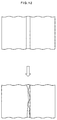
- a correction pattern element may not be sufficient depending on the wiring pattern density, or there is a case that a short circuit is caused between adjacent pattern elements.
- a distance (space width) between two pattern elements is as small as 0.2 to 0.3 micrometers, the space width fluctuates during a light exposure, and there may be caused a short circuit between the two pattern elements as shown in Fig. 12.
- the light exposure pattern mask according to the present invention includes a wiring pattern for forming a wiring pattern of an integrated circuit apparatus and a dummy pattern for forming a dummy pattern in the vicinity of the end portions of the wiring pattern elements.
- the dummy pattern preferably forms a dummy pattern in the vicinity of the end portions of linear elements of the wiring pattern having a width of 0.3 micrometers or below. Moreover, it is preferable that the dummy pattern be a dot-shaped dummy pattern having an identical width as the aforementioned linear element.
- Fig. 1A shows a desired wiring pattern 103 which is used for radiation of a phtoresist surface..
- Fig. 2 shows a light exposure pattern mask 500 having a wiring mask pattern 503 identical to the wiring pattern 103 but enlarged by five times and a dummy mask pattern 501.
- This mask 500 has an area of light transmission and an area of light shading.
- the hatched regions are the areas of light shading.
- the wiring mask pattern 503 and the dummy mask pattern 501 belong to areas to be shaded. That is, this mask 500 is applied to a photoresist using a positive-type photo-sensitive material.
- the wiring mask pattern 503 and the dummy mask pattern 501 belong to areas of light transmission.
- the aforementioned mask forms the desired wiring pattern of Fig. 1 together with dot-shape dummy pattern elements 101 as shown in Fig. 1B.
- This dummy pattern prevents disconnection or short circuit which are often caused by the exposure pattern fluctuation when a plurality of pattern elements are arranged too close to each other.
- the dummy pattern consists of dummy pattern elements 501, each of which is arranged at a position in the vicinity of an end portion of each wiring pattern element 503 formed in a linear shape with the smallest design width of the integrated circuit apparatus.
- the smallest design width when exposed on a circuit board is 0.2 to 0.3 micrometers.
- the dummy pattern exhibits more effect as the width is reduced, for example, to 0.05 micrometers.
- the dummy pattern consists of dummy pattern elements of a square shape with a side length equal to or near the aforementioned width of the linear element. Moreover, an interval between a wiring pattern element and a dummy pattern element is also set to be equal to or near the aforementioned with of the linear element.
- the wiring pattern elements 103 are arranged on a grid 110 formed with an interval twice as much as the width of the linear portion.
- the light exposure mask 500 has the dummy pattern elements 501 with dimensions five times as large as the pattern elements to be formed on the actual circuit.
- a setting data of the wiring pattern 103 is created.
- a data on the end portion of pattern elements having a linear portion of width equal to or below 0.3 micrometers According to this data, a position data is set for each of the dummy pattern elements.
- the light exposure mask 500 is produced.
- the aforementioned setting data of the wiring pattern includes the position data of the end portions of the wiring pattern elements 103 having a linear portions and a width data of the linear portions.
- the position data is set so as to arrange the wiring pattern elements 103 on a grid formed at an identical interval in two directions.
- each of the dummy pattern elements has a square shape having a side length equal to a corresponding end portion of the linear portion.
- each of the dummy pattern elements is formed at a distance equal to the width of the end portion of the linear portion.
- step S3 the setting data of a desired wiring pattern 103 is created.
- step S2 a data is collected on the position coordinates of each end portion of the wiring pattern elements.
- step S3 a coordinate 102 of the end portion of the linear portion having a width of 0.3 micrometers or below (see Fig. 1B).
- step S4 a position data of the dummy pattern element 101 is set according to the coordinates 102 of the end portion, i.e., at both sides of the end portion and at a position opposing to the end portion.
- the dummy pattern elements 101 are set in a square form an exposure pattern consisting of a wiring pattern and a dummy pattern is formed according to the setting data of the wiring pattern 103 and the position data of the dummy pattern 101.
- This mask pattern is on a scale five times greater than the final actual wiring pattern to be obtained.
- the present invention there is no need of checking the wiring pattern density. Moreover, the dummy pattern elements arranged apart from the wiring pattern cause no danger of short circuits compared with the conventional correction elements.
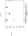
- Fig. 4 shows production yields having no short circuit (indicated by a black circle) or disconnection (indicated by a white circle) for a conventional product, a conventional product having correction pattern elements, and a product produced according to the present invention.
- the present invention enables to significantly enhance the production yield of a semiconductor integrated circuit apparatus having a multiple-layer high-density configuration.
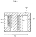
- Fig. 5A shows a wiring pattern 403 of a desired integrated circuit apparatus. This wiring pattern is obtained using a light exposure mask 600 shown in Fig. 6. This light exposure mask 600 has a wiring pattern 603 five times greater than the size of the desired wiring pattern.
- the wiring pattern 403 consists of pattern elements 403a and 403b arranged at a distance 410.
- this distance 410 is reduced to the smallest design value of an integrated circuit apparatus (i.e., 0.2 to 0.3 micrometers)
- the pattern elements 403a and 403 may be partially connected during a light exposure.
- a slit-shape pattern element 401 is formed in one of the pattern elements 403a and 403b having a width of at least 0.3 micrometers. This prevents connection (short circuit) between the pattern elements 403a and 403b.
- the light exposure mask 600 has an area of light transmission and an area of light shading.
- the hatched area is the light shading area.
- the wiring pattern 603 belongs to the light transmission area and the slit pattern belongs to the light shading area. Accordingly, this mask 600 is used for photoresist using a negative-type photo-sensitive material.
- the pattern elements 403a and 403b are arranged on a grid 420 having an interval of 0.2 to 0.3 micrometers (horizontal grid lines are omitted in the figure.)
- the wiring pattern 403 is designed so that all its pattern elements are located on the grid lines 420. Furthermore, when a wiring pattern element is located over several grid lines, a slit pattern element 401 is formed between the outermost line of the grid lines and the adjacent grid line.
- the wiring pattern 403 is located on the grid lines 420, there is no such case that a necessary wiring pattern element is lost.
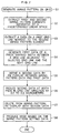
- a setting data of the desired wiring pattern 403 is created so as to be on the grid 420 (step S1, Fig. 8A).
- step S2 Fig. 8B From this setting data is extracted a first wiring pattern element 403a and a second wiring pattern element 403b separated from each other by a space 410 having a width of 0.2 to 0.3 micrometers.
- step S3, Fig. 8C a data on a first grid line 420a nearest to the pattern element 403b is extracted.
- a second grid line 420b belonging to the second wiring pattern element 403b and a third grid line 420c adjacent to the second grid line are extracted.
- a first data 404 is generated so as to form a slit shape having a width of 0.2 to 0.3 micrometers and a length equal to that of the second pattern element 403b (step S4, Fig. 8D).
- a second data 405 is defined by a portion overlapping portion between the data of the wiring pattern element 403b and the first data 404 (step S5, Fig. 8E indicating the second data as a hatched portion).
- Both ends of the second data 405 are respectively reduced by 0.2 to 0.3 micrometers in the longitudinal direction (step S6, Fig. 8F).
- step S7, Fig. 8G From the data on the wiring pattern element 403b is removed such a portion overlapping with the second data 405 so that a slit pattern element 401 is formed between the second grid line 420b and the third grid line 420c (step S7, Fig. 8G).
- step S8 a light exposure mask 600 is formed according to the setting data of the wiring pattern 403 formed according to the aforementioned procedure.
- a slit is formed in the second pattern element 403b.
- a similar operation is carried out.
- the first data is in advance set to a slit shape having a width of 0.3 micrometers or below.
- the aforementioned wiring pattern setting data includes position coordinate data of the end portion of the first and the second pattern elements and a width data of each pattern element.
- the position coordinate data is set so that the aforementioned first and the second wiring pattern element 403a and 403b are located on the grid lines 420.
- the first and the second wiring pattern element have a width which is defined by the number of grid lines 420 used.
- the line interval is assumed to be 0.6 micrometers or below.
- the first data is generated between the second grid line 420b and the third grid lined 420c.
- the slit pattern element 401 is provided in the wider pattern element. This prevents a space fluctuation between the two adjacent pattern elements during a light exposure.
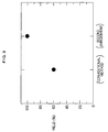
- Fig. 9 shows production yields having no short circuit in the conventional method and the present embodiment. As is clear from Fig. 9, according to the embodiment of the present invention, it is possible to considerably increase the production yield suppressing the generation of short circuits in a semiconductor integrated circuit apparatus having a high-density configuration.
Landscapes
- Physics & Mathematics (AREA)
- General Physics & Mathematics (AREA)
- Engineering & Computer Science (AREA)
- Manufacturing & Machinery (AREA)
- Microelectronics & Electronic Packaging (AREA)
- Preparing Plates And Mask In Photomechanical Process (AREA)
- Exposure And Positioning Against Photoresist Photosensitive Materials (AREA)
- Semiconductor Integrated Circuits (AREA)
Abstract
Description
Claims (29)
- A light exposure pattern mask (500) comprising an integrated circuit wiring pattern consisting of a plurality of wiring pattern elements (503) and a dummy pattern consisting of a plurality of dummy pattern elements (501) provided in the vicinity of ends of said wiring pattern elements.
- A light exposure pattern mask (500) as claimed in Claim 1, wherein said dummy pattern elements (501) are provided in the vicinity of the ends of wiring pattern elements (503) having a linear portion of width when exposed on a circuit board equal to or below 0.3 micrometers.
- A light exposure pattern mask (500) as claimed in Claim 1, wherein said dummy pattern consists of a plurality of dot-shape dummy pattern elements (501).
- A light exposure pattern mask (500) as claimed in Claim 3, wherein said dummy pattern consists of a plurality of square-shape dummy pattern elements (501) having a side length equal to said linear portion width.
- A light exposure pattern mask (500) as claimed in Claim 2, wherein a distance between said dummy pattern elements (501) and said ends of linear portions is equal to said width of said linear portions.
- A light exposure pattern mask (500) as claimed in Claim 1, wherein said wiring pattern elements (503) are provided on a grid(110) formed when exposed on a circuit board at identical intervals in two directions.
- A light exposure pattern mask (500) as claimed in Claim 6, wherein said grid (110) is formed at an interval equal to or below 0.6 micrometers.
- A light exposure pattern mask (500) as claimed in Claim 1, said mask (500) having a light transmitting area and a light shading area, wherein said wiring pattern (503) and said dummy pattern (501) belongs to said light shading area.
- A light exposure pattern mask (500) as claimed in Claim 1, said mask (500) having a light transmitting area and a light shading area, wherein said wiring pattern (503) and said dummy pattern (501) belongs to said light transmitting area.
- A method for producing a light exposure pattern mask (500) having a wiring pattern consisting of a plurality of wiring pattern elements (503) and a dummy pattern consisting of a plurality of dummy pattern elements (501), said method comprising steps of:creating a data for said wiring pattern;extracting from said data on said wiring pattern, ends of wiring pattern elements (503) having a linear portion of width when exposed on a circuit board equal to or below 0.3 micrometers;setting positions of said dummy pattern elements (501) according to said extracted ends; andcreating said dummy pattern from said wiring pattern data and said dummy pattern element position data.
- A method as claimed in Claim 10, wherein said wiring pattern data includes an end position data and a width data of said linear portions.
- A method as claimed in Claim 11, wherein said position data is set so as to arrange said linear portions of said wiring pattern are arranged on a grid (110) having identical intervals.
- A method as claimed in Claim 10, wherein each of said dummy pattern elements (501) is formed in a square shape having a side length equal to said width of said ends of said linear portions.
- A method as claimed in Claim 10, wherein a distance between said dummy pattern elements (501) and corresponding ends of said linear portions is equal to said width of said linear portions.
- A light exposure pattern mask (600) comprising an integrated circuit wiring pattern consisting of a plurality of wiring pattern elements (603), wherein a slit (601) is provided at an end portion of at least one of two adjacent wiring pattern elements (603) arranged parallel to each other at a constant distance.
- A light exposure pattern mask (600) as claimed in Claim 15, wherein said constant distance is when exposed on a circuit board 0.3 micrometers or below.
- A light exposure pattern mask (600) as claimed in Claim 15, wherein said slit (601) has a width when exposed on a circuit board equal to or below 0.3 micrometers.
- A light exposure pattern mask (600) as claimed in Claim 17, wherein said slit (601) is provided for wiring pattern elements (603) having a width when exposed on a circuit board greater than 0.3 micrometers.
- A light exposure pattern mask (600) as claimed in Claim 15, wherein said wiring pattern elements (603) are formed on a grid(420) having identical intervals in two directions.
- A light exposure pattern mask (600) as claimed in Claim 15, wherein said interval when exposed on a circuit board is 0.6 micrometers or below.
- A light exposure pattern mask (600) as claimed in Claim 15, said mask (600) having a light transmitting area and a light shading area, wherein said wiring pattern belongs (603) to said light shading area and said slit (601) belongs to said light transmitting area.
- A light exposure pattern mask (600) as claimed in Claim 15, said mask (600) having a light transmitting area and a light shading area, wherein said wiring pattern(603) belongs to said light transmitting area and said slit (601) belongs to said light shading area.
- A method for producing a light exposure pattern mask having a wiring pattern consisting of a plurality of wiring pattern elements (403), at least one of which has a slit pattern(401) formed in parallel to an adjacent pattern element (403), said method comprising steps of:creating a setting data for said wiring pattern(403);extracting from said setting data on said wiring pattern(403), a first wiring pattern element (403a) and a second wiring pattern element(403b) separated from each other by a linear space having a constant width;according to said first wiring pattern element data, generating a first dummy data (404) at a predetermined distance from the end portion of said wiring pattern element (403);defining a second dummy data(405) by an overlapping portion between said second wiring pattern element data with said firs dummy data(404);reducing the length of said second dummy data (405) at both ends so as to be shorter than said second wiring pattern element(403b);removing the second dummy data (405) portion from said second wiring pattern element(403b) so as to form said slit pattern(401); andcreating said light exposure pattern mask from said setting data of said wiring pattern including said first and said second wiring pattern elements(403a,403b).
- A method as claimed in Claim 23, wherein said second dummy data (405) is reduced in length at both ends when exposed on a circuit board by 0.3 micrometers or less than said second wiring pattern element(403b).
- A method as claimed in Claim 23, wherein said setting data of said first and said second wiring pattern elements(403a,403b) include a position coordinate data of end portions of these pattern elements.
- A method as claimed in Claim 23, wherein said first dummy data (404) has a width of 0.3 micrometers or below.
- A method as claimed in Claim 23, wherein said position coordinate data is set so that said first and said second wiring pattern elements(403a,403b) are located on grid lines (420) arrange at an identical interval.
- A method as claimed in Claim 27, wherein said grid line (420) interval when exposed on a circuit board is set to 0.6 micrometers or below.
- A method as claimed in Claim 27, wherein if said first pattern element (403a) located on a first grid line (420a) has a width smaller than said second pattern element(403b) located over two or more grid lines, said first dummy data(404) is generated between the outermost grid line (second grid line(420b)) and the next line (third grid line(420c)).
Applications Claiming Priority (3)
| Application Number | Priority Date | Filing Date | Title |
|---|---|---|---|
| JP25229297 | 1997-09-17 | ||
| JP252292/97 | 1997-09-17 | ||
| JP25229297A JP3085259B2 (en) | 1997-09-17 | 1997-09-17 | Exposure pattern and method for generating the same |
Publications (2)
| Publication Number | Publication Date |
|---|---|
| EP0903635A2 true EP0903635A2 (en) | 1999-03-24 |
| EP0903635A3 EP0903635A3 (en) | 2000-04-05 |
Family
ID=17235237
Family Applications (1)
| Application Number | Title | Priority Date | Filing Date |
|---|---|---|---|
| EP98117544A Withdrawn EP0903635A3 (en) | 1997-09-17 | 1998-09-16 | Light exposure pattern mask and production method of the same |
Country Status (5)
| Country | Link |
|---|---|
| US (1) | US6197452B1 (en) |
| EP (1) | EP0903635A3 (en) |
| JP (1) | JP3085259B2 (en) |
| KR (1) | KR100309301B1 (en) |
| CN (1) | CN1211813A (en) |
Cited By (2)
| Publication number | Priority date | Publication date | Assignee | Title |
|---|---|---|---|---|
| DE10051719A1 (en) * | 2000-10-18 | 2002-05-08 | Infineon Technologies Ag | Producing circuit structures on semiconducting substrate involves combining first dummy structure with second to exceed minimum size if envisaged structure smaller than minimum |
| WO2004027519A3 (en) * | 2002-09-19 | 2004-09-23 | Infineon Technologies Ag | Dummy patterns for reducing proximity effects and method of using same |
Families Citing this family (30)
| Publication number | Priority date | Publication date | Assignee | Title |
|---|---|---|---|---|
| US6277542B1 (en) | 1998-06-05 | 2001-08-21 | Nikon Corporation | Charged-particle-beam projection-exposure methods exhibiting more uniform beam-current density |
| JP2000349145A (en) * | 1999-04-02 | 2000-12-15 | Oki Electric Ind Co Ltd | Semiconductor device |
| KR100313280B1 (en) * | 1999-10-25 | 2001-11-07 | 한신혁 | Method for producing a mask for a metal line in a semiconductor device |
| JP2002116529A (en) * | 2000-10-06 | 2002-04-19 | Dainippon Printing Co Ltd | Correction method for semiconductor circuit design pattern data and photomask made by pattern data obtained by this correction method |
| KR100378195B1 (en) * | 2001-02-21 | 2003-03-29 | 삼성전자주식회사 | Generation method of data for used in mask including dummy pattern groups having density continuously adjusted in according to density of local design pattern and recording media in which the same recorded |
| DE10127689B4 (en) * | 2001-06-08 | 2005-07-07 | Infineon Technologies Ag | Method for producing scattering lines in mask structures for the production of integrated electrical circuits |
| KR100419870B1 (en) * | 2001-06-27 | 2004-02-25 | 주식회사 하이닉스반도체 | A method for fabricating metal line |
| US6887633B2 (en) * | 2002-02-08 | 2005-05-03 | Chih-Hsien Nail Tang | Resolution enhancing technology using phase assignment bridges |
| US7252909B2 (en) * | 2002-04-18 | 2007-08-07 | Taiwan Semiconductor Manufacturing Co., Ltd. | Method to reduce CD non-uniformity in IC manufacturing |
| US6929887B1 (en) | 2002-04-18 | 2005-08-16 | Taiwan Semiconductor Manufacturing Co., Ltd. | Printable assist lines and the removal of such |
| DE10240403A1 (en) * | 2002-09-02 | 2004-03-11 | Infineon Technologies Ag | Mask for projecting a structural pattern onto a semiconductor substrate in an exposure device comprises a substrate, a first structural element on the substrate, and an arrangement of second structural elements |
| JP4109944B2 (en) * | 2002-09-20 | 2008-07-02 | キヤノン株式会社 | Method for manufacturing solid-state imaging device |
| CN1299164C (en) * | 2003-04-08 | 2007-02-07 | 旺宏电子股份有限公司 | Method for Eliminating Deviation of Critical Dimensions Between Dense Patterns and Single Patterns |
| US7097945B2 (en) * | 2003-04-18 | 2006-08-29 | Macronix International Co., Ltd. | Method of reducing critical dimension bias of dense pattern and isolation pattern |
| KR100546119B1 (en) * | 2003-10-23 | 2006-01-24 | 주식회사 하이닉스반도체 | How do you improve the uniformity and alignment accuracy of your array contacts? |
| JP2006019577A (en) * | 2004-07-02 | 2006-01-19 | Fujitsu Ltd | Exposure mask and method of manufacturing semiconductor device |
| JP4768980B2 (en) * | 2004-10-28 | 2011-09-07 | ルネサスエレクトロニクス株式会社 | Exposure mask and wiring layer mask pattern design method |
| US20070281218A1 (en) * | 2006-06-02 | 2007-12-06 | Howard S Landis | Dummy Phase Shapes To Reduce Sensitivity Of Critical Gates To Regions Of High Pattern Density |
| US7858269B2 (en) * | 2007-03-16 | 2010-12-28 | International Business Machines Corporation | Structure and method for sub-resolution dummy clear shapes for improved gate dimensional control |
| KR100847844B1 (en) | 2007-08-10 | 2008-07-23 | 주식회사 동부하이텍 | Dummy pattern design method of semiconductor device |
| KR100853801B1 (en) | 2007-08-23 | 2008-08-25 | 주식회사 동부하이텍 | Mask of semiconductor device and patterning method using same |
| JP5415710B2 (en) * | 2008-04-10 | 2014-02-12 | ルネサスエレクトロニクス株式会社 | Semiconductor device |
| JP5235936B2 (en) | 2010-05-10 | 2013-07-10 | パナソニック株式会社 | Semiconductor device and layout creation method thereof |
| US8941185B2 (en) * | 2011-02-09 | 2015-01-27 | Sharp Kabushiki Kaisha | Active matrix substrate, x-ray sensor device, display device |
| TWI440965B (en) * | 2011-09-05 | 2014-06-11 | Au Optronics Corp | Photomask, manufacturing method of conducting wiring of flat display panel and wiring structure of flat display panel |
| KR101919467B1 (en) | 2012-05-08 | 2019-02-11 | 삼성디스플레이 주식회사 | Mask and mask assembly having the same |
| CN103050379B (en) * | 2012-12-10 | 2015-03-04 | 华映视讯(吴江)有限公司 | Method for forming narrow-pitch lines |
| CN106569395B (en) * | 2015-10-08 | 2018-06-15 | 无锡华润上华科技有限公司 | Measure the photomask and method of exposure bench light leakage |
| CN110221515B (en) * | 2018-03-02 | 2023-01-20 | 中芯国际集成电路制造(上海)有限公司 | Optical proximity correction method and manufacturing method of mask |
| KR102879037B1 (en) | 2020-08-19 | 2025-10-29 | 삼성전자주식회사 | semiconductor device including patterns |
Family Cites Families (26)
| Publication number | Priority date | Publication date | Assignee | Title |
|---|---|---|---|---|
| JPS62141558A (en) | 1985-12-16 | 1987-06-25 | Oki Electric Ind Co Ltd | Photomask and formation of fine pattern using said mask |
| JPS63211739A (en) | 1987-02-27 | 1988-09-02 | Nec Corp | semiconductor equipment |
| JPS6459832A (en) * | 1987-08-31 | 1989-03-07 | Toshiba Corp | Manufacture of semiconductor device |
| JPH01195450A (en) | 1988-01-29 | 1989-08-07 | Matsushita Electric Ind Co Ltd | Photomask pattern producing method |
| JPH01302256A (en) | 1988-05-30 | 1989-12-06 | Sharp Corp | Photomask for rectangular pattern resolution |
| JPH04215656A (en) | 1990-12-14 | 1992-08-06 | Fujitsu Ltd | Forming method for ic pattern |
| JPH04216548A (en) | 1990-12-18 | 1992-08-06 | Mitsubishi Electric Corp | photo mask |
| JPH04251253A (en) | 1991-01-09 | 1992-09-07 | Fujitsu Ltd | Exposing mask |
| JP3179520B2 (en) | 1991-07-11 | 2001-06-25 | 株式会社日立製作所 | Method for manufacturing semiconductor device |
| US5242770A (en) | 1992-01-16 | 1993-09-07 | Microunity Systems Engineering, Inc. | Mask for photolithography |
| JPH05204132A (en) | 1992-01-27 | 1993-08-13 | Fujitsu Ltd | Reticule and its production |
| JP3194155B2 (en) * | 1992-01-31 | 2001-07-30 | キヤノン株式会社 | Semiconductor device manufacturing method and projection exposure apparatus using the same |
| US5256505A (en) * | 1992-08-21 | 1993-10-26 | Microunity Systems Engineering | Lithographical mask for controlling the dimensions of resist patterns |
| JP3129007B2 (en) | 1992-12-11 | 2001-01-29 | 株式会社日立製作所 | Photomask and method for manufacturing semiconductor device |
| JPH07134395A (en) * | 1993-04-22 | 1995-05-23 | Samsung Electron Co Ltd | Mask pattern and method of forming fine pattern using the same |
| JPH0764274A (en) | 1993-08-30 | 1995-03-10 | Sony Corp | Phase shift mask and manufacturing method thereof |
| JP3334339B2 (en) | 1994-06-23 | 2002-10-15 | 富士通株式会社 | Semiconductor device wiring layout method and manufacturing method |
| KR960005756A (en) | 1994-07-28 | 1996-02-23 | 김주용 | Photomask Manufacturing Method for Semiconductor Device Manufacturing |
| JP3249317B2 (en) | 1994-12-12 | 2002-01-21 | 富士通株式会社 | Pattern creation method |
| KR0172561B1 (en) * | 1995-06-23 | 1999-03-30 | 김주용 | Suppressing Proximity Effect of a Lag Mask |
| JPH0915833A (en) * | 1995-06-30 | 1997-01-17 | Sony Corp | Scanning data creating apparatus and scanning data creating method in exposure mask manufacturing apparatus |
| JP2917879B2 (en) * | 1995-10-31 | 1999-07-12 | 日本電気株式会社 | Photomask and manufacturing method thereof |
| JPH09180978A (en) * | 1995-12-27 | 1997-07-11 | Nikon Corp | Proximity effect correction method |
| US5705301A (en) * | 1996-02-27 | 1998-01-06 | Lsi Logic Corporation | Performing optical proximity correction with the aid of design rule checkers |
| JP2998661B2 (en) | 1996-11-11 | 2000-01-11 | 日本電気株式会社 | Photomask and pattern forming method for semiconductor device |
| US5900340A (en) * | 1997-03-03 | 1999-05-04 | Motorola, Inc. | One dimensional lithographic proximity correction using DRC shape functions |
-
1997
- 1997-09-17 JP JP25229297A patent/JP3085259B2/en not_active Expired - Fee Related
-
1998
- 1998-09-16 US US09/154,036 patent/US6197452B1/en not_active Expired - Fee Related
- 1998-09-16 EP EP98117544A patent/EP0903635A3/en not_active Withdrawn
- 1998-09-16 KR KR1019980038248A patent/KR100309301B1/en not_active Expired - Fee Related
- 1998-09-17 CN CN98119343A patent/CN1211813A/en active Pending
Cited By (4)
| Publication number | Priority date | Publication date | Assignee | Title |
|---|---|---|---|---|
| DE10051719A1 (en) * | 2000-10-18 | 2002-05-08 | Infineon Technologies Ag | Producing circuit structures on semiconducting substrate involves combining first dummy structure with second to exceed minimum size if envisaged structure smaller than minimum |
| US6586308B2 (en) | 2000-10-18 | 2003-07-01 | Infineon Technologies Ag | Method for producing circuit structures on a semiconductor substrate and semiconductor configuration with functional circuit structures and dummy circuit structures |
| DE10051719C2 (en) * | 2000-10-18 | 2003-10-02 | Infineon Technologies Ag | Process for the production of circuit structures on a semiconductor substrate with the aid of a lithography process and arrangement with functional circuit structures and dummy circuit structures |
| WO2004027519A3 (en) * | 2002-09-19 | 2004-09-23 | Infineon Technologies Ag | Dummy patterns for reducing proximity effects and method of using same |
Also Published As
| Publication number | Publication date |
|---|---|
| US6197452B1 (en) | 2001-03-06 |
| JPH1195406A (en) | 1999-04-09 |
| JP3085259B2 (en) | 2000-09-04 |
| KR19990029853A (en) | 1999-04-26 |
| EP0903635A3 (en) | 2000-04-05 |
| CN1211813A (en) | 1999-03-24 |
| KR100309301B1 (en) | 2001-11-15 |
Similar Documents
| Publication | Publication Date | Title |
|---|---|---|
| EP0903635A2 (en) | Light exposure pattern mask and production method of the same | |
| JP3311244B2 (en) | Basic cell library and method of forming the same | |
| JP4346410B2 (en) | Wiring design method for semiconductor integrated circuit and semiconductor integrated circuit | |
| US6779167B2 (en) | Automated wiring pattern layout method | |
| KR100384805B1 (en) | Semiconductor device, design method and recording media storing design program of the same | |
| US5610831A (en) | Semiconductor element layout method employing process migration | |
| KR100608117B1 (en) | Exposing method and apparatus for semiconductor integrated circuits | |
| US7859111B2 (en) | Computer implemented method for designing a semiconductor device, an automated design system and a semiconductor device | |
| KR20020065851A (en) | Method for correcting optical proximity effects | |
| US5008830A (en) | Method of preparing drawing data for charged beam exposure system | |
| GB2344436A (en) | Method of manufacture of a semiconductor device | |
| CN100592494C (en) | Method of Correcting Layout Design of Contact Hole Metal Covering Layer | |
| US6892372B2 (en) | Wiring layout method of integrated circuit | |
| DE102021104603B4 (en) | CORNER STRUCTURES FOR AN OPTICAL FIBER GROOVE AND METHOD | |
| DE10356693A1 (en) | A method of generating an aberration avoiding mask layout for a mask | |
| JP3659242B2 (en) | Mask pattern correction method | |
| CN117492332A (en) | A layout graphics splitting method, device and computer equipment | |
| JP2004294664A (en) | Reticle creation method and reticle creation program | |
| JPH10256255A (en) | Pattern generation method for semiconductor integrated circuit device | |
| JP4209577B2 (en) | Via formation region determination method | |
| KR100280248B1 (en) | Automatic arrangement of wiring patterns in semiconductor device | |
| JP3606144B2 (en) | Printed circuit board design system | |
| JP3468823B2 (en) | Screen in screen printing | |
| US5917206A (en) | Gate array system in which functional blocks are connected by fixed wiring | |
| JPH06124322A (en) | Wiring method for specified length net |
Legal Events
| Date | Code | Title | Description |
|---|---|---|---|
| PUAI | Public reference made under article 153(3) epc to a published international application that has entered the european phase |
Free format text: ORIGINAL CODE: 0009012 |
|
| AK | Designated contracting states |
Kind code of ref document: A2 Designated state(s): DE GB |
|
| AX | Request for extension of the european patent |
Free format text: AL;LT;LV;MK;RO;SI |
|
| PUAL | Search report despatched |
Free format text: ORIGINAL CODE: 0009013 |
|
| AK | Designated contracting states |
Kind code of ref document: A3 Designated state(s): AT BE CH CY DE DK ES FI FR GB GR IE IT LI LU MC NL PT SE |
|
| AX | Request for extension of the european patent |
Free format text: AL;LT;LV;MK;RO;SI |
|
| RIC1 | Information provided on ipc code assigned before grant |
Free format text: 7G 03F 1/14 A, 7G 03F 7/20 B |
|
| 17P | Request for examination filed |
Effective date: 20000508 |
|
| AKX | Designation fees paid |
Free format text: DE GB |
|
| STAA | Information on the status of an ep patent application or granted ep patent |
Free format text: STATUS: THE APPLICATION HAS BEEN WITHDRAWN |
|
| RAP1 | Party data changed (applicant data changed or rights of an application transferred) |
Owner name: NEC ELECTRONICS CORPORATION |
|
| 18W | Application withdrawn |
Effective date: 20030331 |