EP0903614A2 - Flüssigkristallanzeigevorrichtung mit weitem Sehfeld - Google Patents
Flüssigkristallanzeigevorrichtung mit weitem Sehfeld Download PDFInfo
- Publication number
- EP0903614A2 EP0903614A2 EP98117670A EP98117670A EP0903614A2 EP 0903614 A2 EP0903614 A2 EP 0903614A2 EP 98117670 A EP98117670 A EP 98117670A EP 98117670 A EP98117670 A EP 98117670A EP 0903614 A2 EP0903614 A2 EP 0903614A2
- Authority
- EP
- European Patent Office
- Prior art keywords
- alignment film
- liquid crystal
- alignment
- molecules
- degrees
- Prior art date
- Legal status (The legal status is an assumption and is not a legal conclusion. Google has not performed a legal analysis and makes no representation as to the accuracy of the status listed.)
- Withdrawn
Links
- 239000004973 liquid crystal related substance Substances 0.000 title claims abstract description 44
- 238000011282 treatment Methods 0.000 claims abstract description 37
- 239000000758 substrate Substances 0.000 claims description 27
- 230000005684 electric field Effects 0.000 claims description 10
- 238000000034 method Methods 0.000 claims description 7
- 238000004519 manufacturing process Methods 0.000 abstract description 2
- 239000010408 film Substances 0.000 description 68
- 239000011521 glass Substances 0.000 description 12
- 238000009413 insulation Methods 0.000 description 6
- 238000002161 passivation Methods 0.000 description 3
- 239000011159 matrix material Substances 0.000 description 2
- 239000013598 vector Substances 0.000 description 2
- 238000010521 absorption reaction Methods 0.000 description 1
- 210000001520 comb Anatomy 0.000 description 1
- 238000007796 conventional method Methods 0.000 description 1
- 238000002474 experimental method Methods 0.000 description 1
- 238000006467 substitution reaction Methods 0.000 description 1
- 239000010409 thin film Substances 0.000 description 1
- 238000002834 transmittance Methods 0.000 description 1
Images


Classifications
-
- G—PHYSICS
- G02—OPTICS
- G02F—OPTICAL DEVICES OR ARRANGEMENTS FOR THE CONTROL OF LIGHT BY MODIFICATION OF THE OPTICAL PROPERTIES OF THE MEDIA OF THE ELEMENTS INVOLVED THEREIN; NON-LINEAR OPTICS; FREQUENCY-CHANGING OF LIGHT; OPTICAL LOGIC ELEMENTS; OPTICAL ANALOGUE/DIGITAL CONVERTERS
- G02F1/00—Devices or arrangements for the control of the intensity, colour, phase, polarisation or direction of light arriving from an independent light source, e.g. switching, gating or modulating; Non-linear optics
- G02F1/01—Devices or arrangements for the control of the intensity, colour, phase, polarisation or direction of light arriving from an independent light source, e.g. switching, gating or modulating; Non-linear optics for the control of the intensity, phase, polarisation or colour
- G02F1/13—Devices or arrangements for the control of the intensity, colour, phase, polarisation or direction of light arriving from an independent light source, e.g. switching, gating or modulating; Non-linear optics for the control of the intensity, phase, polarisation or colour based on liquid crystals, e.g. single liquid crystal display cells
- G02F1/133—Constructional arrangements; Operation of liquid crystal cells; Circuit arrangements
- G02F1/1333—Constructional arrangements; Manufacturing methods
- G02F1/1343—Electrodes
- G02F1/134309—Electrodes characterised by their geometrical arrangement
- G02F1/134363—Electrodes characterised by their geometrical arrangement for applying an electric field parallel to the substrate, i.e. in-plane switching [IPS]
-
- G—PHYSICS
- G02—OPTICS
- G02F—OPTICAL DEVICES OR ARRANGEMENTS FOR THE CONTROL OF LIGHT BY MODIFICATION OF THE OPTICAL PROPERTIES OF THE MEDIA OF THE ELEMENTS INVOLVED THEREIN; NON-LINEAR OPTICS; FREQUENCY-CHANGING OF LIGHT; OPTICAL LOGIC ELEMENTS; OPTICAL ANALOGUE/DIGITAL CONVERTERS
- G02F1/00—Devices or arrangements for the control of the intensity, colour, phase, polarisation or direction of light arriving from an independent light source, e.g. switching, gating or modulating; Non-linear optics
- G02F1/01—Devices or arrangements for the control of the intensity, colour, phase, polarisation or direction of light arriving from an independent light source, e.g. switching, gating or modulating; Non-linear optics for the control of the intensity, phase, polarisation or colour
- G02F1/13—Devices or arrangements for the control of the intensity, colour, phase, polarisation or direction of light arriving from an independent light source, e.g. switching, gating or modulating; Non-linear optics for the control of the intensity, phase, polarisation or colour based on liquid crystals, e.g. single liquid crystal display cells
- G02F1/133—Constructional arrangements; Operation of liquid crystal cells; Circuit arrangements
- G02F1/1333—Constructional arrangements; Manufacturing methods
- G02F1/1335—Structural association of cells with optical devices, e.g. polarisers or reflectors
- G02F1/13363—Birefringent elements, e.g. for optical compensation
-
- G—PHYSICS
- G02—OPTICS
- G02F—OPTICAL DEVICES OR ARRANGEMENTS FOR THE CONTROL OF LIGHT BY MODIFICATION OF THE OPTICAL PROPERTIES OF THE MEDIA OF THE ELEMENTS INVOLVED THEREIN; NON-LINEAR OPTICS; FREQUENCY-CHANGING OF LIGHT; OPTICAL LOGIC ELEMENTS; OPTICAL ANALOGUE/DIGITAL CONVERTERS
- G02F1/00—Devices or arrangements for the control of the intensity, colour, phase, polarisation or direction of light arriving from an independent light source, e.g. switching, gating or modulating; Non-linear optics
- G02F1/01—Devices or arrangements for the control of the intensity, colour, phase, polarisation or direction of light arriving from an independent light source, e.g. switching, gating or modulating; Non-linear optics for the control of the intensity, phase, polarisation or colour
- G02F1/13—Devices or arrangements for the control of the intensity, colour, phase, polarisation or direction of light arriving from an independent light source, e.g. switching, gating or modulating; Non-linear optics for the control of the intensity, phase, polarisation or colour based on liquid crystals, e.g. single liquid crystal display cells
- G02F1/133—Constructional arrangements; Operation of liquid crystal cells; Circuit arrangements
- G02F1/1333—Constructional arrangements; Manufacturing methods
- G02F1/1337—Surface-induced orientation of the liquid crystal molecules, e.g. by alignment layers
- G02F1/133753—Surface-induced orientation of the liquid crystal molecules, e.g. by alignment layers with different alignment orientations or pretilt angles on a same surface, e.g. for grey scale or improved viewing angle
-
- G—PHYSICS
- G02—OPTICS
- G02F—OPTICAL DEVICES OR ARRANGEMENTS FOR THE CONTROL OF LIGHT BY MODIFICATION OF THE OPTICAL PROPERTIES OF THE MEDIA OF THE ELEMENTS INVOLVED THEREIN; NON-LINEAR OPTICS; FREQUENCY-CHANGING OF LIGHT; OPTICAL LOGIC ELEMENTS; OPTICAL ANALOGUE/DIGITAL CONVERTERS
- G02F1/00—Devices or arrangements for the control of the intensity, colour, phase, polarisation or direction of light arriving from an independent light source, e.g. switching, gating or modulating; Non-linear optics
- G02F1/01—Devices or arrangements for the control of the intensity, colour, phase, polarisation or direction of light arriving from an independent light source, e.g. switching, gating or modulating; Non-linear optics for the control of the intensity, phase, polarisation or colour
- G02F1/13—Devices or arrangements for the control of the intensity, colour, phase, polarisation or direction of light arriving from an independent light source, e.g. switching, gating or modulating; Non-linear optics for the control of the intensity, phase, polarisation or colour based on liquid crystals, e.g. single liquid crystal display cells
- G02F1/133—Constructional arrangements; Operation of liquid crystal cells; Circuit arrangements
- G02F1/1333—Constructional arrangements; Manufacturing methods
- G02F1/1337—Surface-induced orientation of the liquid crystal molecules, e.g. by alignment layers
- G02F1/133749—Surface-induced orientation of the liquid crystal molecules, e.g. by alignment layers for low pretilt angles, i.e. lower than 15 degrees
Definitions
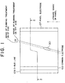
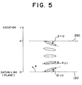
- both of the first and second predetermined ranges are selected between three degrees and eight degrees, both inclusive.
- a refraction anisotropy at one location differs from the other refraction anisotropy at the other location. Therefore, in this specification, a concept of an effective refraction anisotropy ⁇ n' is introduced when a refraction anisotropy is variable with the variable location z.
- the effective refraction anisotropy ⁇ n' is represented by Equation (5) in connection with the pretilt angle of the molecule at the variable location z and both refractive indexes n e and n o of long and short axes of the molecule.
- ⁇ n'(z) n e n o n e 2 sin ⁇ (z) + n o 2 cos ⁇ (z) - n 0
- the light transmittance T/T 0 is generally represented by Equation (7).
- T T 0 sin 2 (2 ⁇ )sin 2 ( ⁇ nd / ⁇ ) where ⁇ represents a wavelength of light transparent into the liquid crystal layer, ⁇ nd represents a general retardation, and ⁇ represents an angle between the director of each molecule and the poralizer absorption axis.
- the above general retardation ⁇ nd is replaced by the effective retardation R eff .
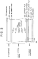
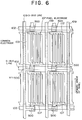
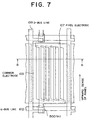
- the TFT array substrate 100 has a glass plate 101, a common electrode 103, a gate insulation film 105, a pixel electrode 107, a D-bus line 109, and a passivation film 111.
- the common electrode 103, the gate insulation film 105, the pixel electrode 107 and the D-bus line 109 are all formed on one side of the glass plate 101.
- the passivation film 111 covers all over the gate insulation film 105, the pixel electrode 107 and the D-bus line 109.
- the common electrode 103, the pixel electrode 107, and the D-bus line 109 all have parts extended in the upward sense of the panel.
- the alignment film 130 covers all over the passivation film 111.
- a surface of the TFT array substrate 100, on which the alignment film 130 is formed, is referred to as a first principal surface.
- a polarizer 140 is formed on the other side of the glass plate 101, opposite to the first principal surface.
Landscapes
- Physics & Mathematics (AREA)
- Nonlinear Science (AREA)
- Mathematical Physics (AREA)
- Chemical & Material Sciences (AREA)
- Crystallography & Structural Chemistry (AREA)
- General Physics & Mathematics (AREA)
- Optics & Photonics (AREA)
- Geometry (AREA)
- Liquid Crystal (AREA)
- Spectroscopy & Molecular Physics (AREA)
Applications Claiming Priority (3)
| Application Number | Priority Date | Filing Date | Title |
|---|---|---|---|
| JP252060/97 | 1997-09-17 | ||
| JP25206097A JP3212920B2 (ja) | 1997-09-17 | 1997-09-17 | 液晶表示装置 |
| JP25206097 | 1997-09-17 |
Publications (2)
| Publication Number | Publication Date |
|---|---|
| EP0903614A2 true EP0903614A2 (de) | 1999-03-24 |
| EP0903614A3 EP0903614A3 (de) | 1999-12-29 |
Family
ID=17232008
Family Applications (1)
| Application Number | Title | Priority Date | Filing Date |
|---|---|---|---|
| EP98117670A Withdrawn EP0903614A3 (de) | 1997-09-17 | 1998-09-17 | Flüssigkristallanzeigevorrichtung mit weitem Sehfeld |
Country Status (5)
| Country | Link |
|---|---|
| US (1) | US6078375A (de) |
| EP (1) | EP0903614A3 (de) |
| JP (1) | JP3212920B2 (de) |
| KR (1) | KR100326826B1 (de) |
| TW (1) | TW461983B (de) |
Cited By (2)
| Publication number | Priority date | Publication date | Assignee | Title |
|---|---|---|---|---|
| US6867835B2 (en) * | 2000-08-28 | 2005-03-15 | Lg. Philips Lcd Co., Ltd. | In-plane switching LCD panel having different alignment layers |
| WO2014131774A1 (de) * | 2013-02-27 | 2014-09-04 | Seereal Technologies S.A. | Optischer flüssigkristall-phasenmodulator |
Families Citing this family (18)
| Publication number | Priority date | Publication date | Assignee | Title |
|---|---|---|---|---|
| JP2991995B2 (ja) * | 1997-07-14 | 1999-12-20 | 三菱電機株式会社 | 液晶表示装置 |
| JP3267224B2 (ja) * | 1997-12-26 | 2002-03-18 | 日本電気株式会社 | アクティブマトリクス型液晶表示装置 |
| KR100543027B1 (ko) * | 1998-04-03 | 2006-04-12 | 삼성전자주식회사 | 평면 구동 방식 액정 표시 장치 |
| JP3481509B2 (ja) * | 1999-06-16 | 2003-12-22 | Nec液晶テクノロジー株式会社 | 液晶表示装置 |
| WO2001009675A1 (en) * | 1999-07-29 | 2001-02-08 | Matsushita Electric Industrial Co., Ltd. | Liquid crystal display device and method for manufacturing the same |
| JP2001281671A (ja) * | 2000-03-30 | 2001-10-10 | Hitachi Ltd | 液晶表示装置 |
| KR20010108844A (ko) * | 2000-05-31 | 2001-12-08 | 주식회사 현대 디스플레이 테크놀로지 | 프린지 필드 구동 액정 표시 장치 |
| US6459464B1 (en) * | 2000-08-14 | 2002-10-01 | Kabushiki Kaisha Advanced Display | Liquid crystal display device with reduced weighting trace defects |
| KR100674231B1 (ko) * | 2000-12-05 | 2007-01-25 | 비오이 하이디스 테크놀로지 주식회사 | 프린지 필드 구동 모드 액정 표시 장치 |
| KR100752505B1 (ko) * | 2000-12-30 | 2007-08-28 | 엘지.필립스 엘시디 주식회사 | 강유전성 액정표시장치 |
| KR20040036953A (ko) * | 2002-10-25 | 2004-05-04 | 삼성전자주식회사 | 액정 표시 장치 |
| US7289179B2 (en) * | 2002-11-08 | 2007-10-30 | Samsung Electronics Co., Ltd. | Liquid crystal display |
| KR100601916B1 (ko) | 2003-11-21 | 2006-07-14 | 주식회사 엘지화학 | 양의 이축성 위상차 필름을 이용한 시야각 보상필름을포함하는 면상 스위칭 액정 표시장치 |
| KR100565948B1 (ko) * | 2003-12-11 | 2006-03-30 | 엘지.필립스 엘시디 주식회사 | 횡전계형 액정표시장치의 액정셀 공정 |
| US7014914B2 (en) | 2004-01-09 | 2006-03-21 | Milliken & Company | Polyester yarn and airbags employing certain polyester yarn |
| GB2451552B (en) * | 2007-07-20 | 2010-08-04 | Lg Display Co Ltd | Liquid crystal display device of in-plane switching mode and method for manufacturing the same |
| KR102395574B1 (ko) * | 2015-12-04 | 2022-05-06 | 엘지디스플레이 주식회사 | 액정표시장치 |
| CN113687544A (zh) * | 2020-05-18 | 2021-11-23 | 京东方科技集团股份有限公司 | 显示面板及其制备方法、显示装置 |
Family Cites Families (7)
| Publication number | Priority date | Publication date | Assignee | Title |
|---|---|---|---|---|
| DE4000451B4 (de) * | 1990-01-09 | 2004-12-09 | Merck Patent Gmbh | Elektrooptisches Flüssigkristallschaltelement |
| DE69333323T2 (de) * | 1992-09-18 | 2004-09-16 | Hitachi, Ltd. | Flüssigkristall-Anzeigevorrichtung |
| DE19537802A1 (de) * | 1995-10-11 | 1997-04-17 | Merck Patent Gmbh | Elektrooptische Flüssigkristallanzeige |
| JPH0980436A (ja) * | 1995-09-08 | 1997-03-28 | Hosiden Corp | 液晶表示素子 |
| JP2973934B2 (ja) * | 1996-07-11 | 1999-11-08 | 日本電気株式会社 | 液晶表示装置、及び液晶表示装置を搭載した電子機器 |
| KR100236518B1 (ko) * | 1996-09-21 | 2000-01-15 | 구본준 | 액정표시장치 |
| JPH09230364A (ja) * | 1997-03-18 | 1997-09-05 | Hitachi Ltd | 液晶表示装置 |
-
1997
- 1997-09-17 JP JP25206097A patent/JP3212920B2/ja not_active Expired - Fee Related
-
1998
- 1998-09-15 KR KR1019980037915A patent/KR100326826B1/ko not_active Expired - Lifetime
- 1998-09-16 US US09/154,039 patent/US6078375A/en not_active Expired - Lifetime
- 1998-09-17 EP EP98117670A patent/EP0903614A3/de not_active Withdrawn
- 1998-09-17 TW TW087115488A patent/TW461983B/zh not_active IP Right Cessation
Cited By (5)
| Publication number | Priority date | Publication date | Assignee | Title |
|---|---|---|---|---|
| US6867835B2 (en) * | 2000-08-28 | 2005-03-15 | Lg. Philips Lcd Co., Ltd. | In-plane switching LCD panel having different alignment layers |
| US7196757B2 (en) | 2000-08-28 | 2007-03-27 | Lg.Philips Lcd Co., Ltd. | In-plane switching LCD panel having different alignment layers |
| WO2014131774A1 (de) * | 2013-02-27 | 2014-09-04 | Seereal Technologies S.A. | Optischer flüssigkristall-phasenmodulator |
| US9671649B2 (en) | 2013-02-27 | 2017-06-06 | Seereal Technologies S.A. | Optical liquid-crystal phase modulator |
| US10268080B2 (en) | 2013-02-27 | 2019-04-23 | Seereal Technologies S.A. | Optical liquid-crystal phase modulator |
Also Published As
| Publication number | Publication date |
|---|---|
| TW461983B (en) | 2001-11-01 |
| JPH1195218A (ja) | 1999-04-09 |
| KR100326826B1 (ko) | 2002-06-20 |
| EP0903614A3 (de) | 1999-12-29 |
| US6078375A (en) | 2000-06-20 |
| JP3212920B2 (ja) | 2001-09-25 |
| KR19990029793A (ko) | 1999-04-26 |
Similar Documents
| Publication | Publication Date | Title |
|---|---|---|
| US6078375A (en) | Liquid crystal display device with wide viewing angle | |
| US5309264A (en) | Liquid crystal displays having multi-domain cells | |
| US6987551B2 (en) | In-plane switching liquid crystal display unit having tinting compensation | |
| US6778245B2 (en) | Liquid crystal display device | |
| US7057696B2 (en) | In-plane switching LCD panel with particular discontinuous auxiliary electrodes | |
| US7932980B2 (en) | Liquid crystal display device having patterned electrodes for repetitive divided horizontal electric field and fringing electric field | |
| US5907380A (en) | Liquid crystal cell employing thin wall for pre-tilt control | |
| US6753551B2 (en) | Liquid crystal display with wide viewing angle | |
| US20030197824A1 (en) | Liquid crystal display | |
| CN101878447A (zh) | 液晶显示装置 | |
| US20040070715A1 (en) | Vertical alignment mode liquid crystal display device | |
| US7956971B2 (en) | Liquid crystal display and electronic device having same | |
| KR20000009518A (ko) | 광시야각을 갖는 수직배향 액정표시소자 | |
| US6593988B1 (en) | Multi-domain liquid crystal display with wall-bump structures in pixel area | |
| US7196757B2 (en) | In-plane switching LCD panel having different alignment layers | |
| JP3061119B2 (ja) | 液晶表示装置 | |
| JPH05173137A (ja) | 液晶表示装置 | |
| US20050105015A1 (en) | Continuous domain vertical alignment liquid crystal display | |
| US12313939B2 (en) | Liquid crystal display apparatus | |
| JP3130686B2 (ja) | 液晶表示素子 | |
| US6600531B1 (en) | Liquid crystal cell | |
| KR100237674B1 (ko) | 시야각을 향상시키는 액정 표시 장치 | |
| KR100860240B1 (ko) | 광굴절부를 구비하는 액정표시장치 | |
| JPH06242448A (ja) | 液晶表示素子 | |
| JPH06324335A (ja) | 液晶表示素子 |
Legal Events
| Date | Code | Title | Description |
|---|---|---|---|
| PUAI | Public reference made under article 153(3) epc to a published international application that has entered the european phase |
Free format text: ORIGINAL CODE: 0009012 |
|
| AK | Designated contracting states |
Kind code of ref document: A2 Designated state(s): DE FR GB |
|
| AX | Request for extension of the european patent |
Free format text: AL;LT;LV;MK;RO;SI |
|
| PUAL | Search report despatched |
Free format text: ORIGINAL CODE: 0009013 |
|
| AK | Designated contracting states |
Kind code of ref document: A3 Designated state(s): AT BE CH CY DE DK ES FI FR GB GR IE IT LI LU MC NL PT SE |
|
| AX | Request for extension of the european patent |
Free format text: AL;LT;LV;MK;RO;SI |
|
| 17P | Request for examination filed |
Effective date: 19991122 |
|
| AKX | Designation fees paid |
Free format text: DE FR GB |
|
| RAP1 | Party data changed (applicant data changed or rights of an application transferred) |
Owner name: NEC LCD TECHNOLOGIES, LTD. |
|
| 17Q | First examination report despatched |
Effective date: 20060320 |
|
| STAA | Information on the status of an ep patent application or granted ep patent |
Free format text: STATUS: THE APPLICATION HAS BEEN WITHDRAWN |
|
| 18W | Application withdrawn |
Effective date: 20070403 |