EP0902961B1 - Verfahren zum behandeln eines scheibens mit einem plasmastrahl - Google Patents
Verfahren zum behandeln eines scheibens mit einem plasmastrahl Download PDFInfo
- Publication number
- EP0902961B1 EP0902961B1 EP97927804A EP97927804A EP0902961B1 EP 0902961 B1 EP0902961 B1 EP 0902961B1 EP 97927804 A EP97927804 A EP 97927804A EP 97927804 A EP97927804 A EP 97927804A EP 0902961 B1 EP0902961 B1 EP 0902961B1
- Authority
- EP
- European Patent Office
- Prior art keywords
- article
- plasma jet
- article surface
- along
- rotation radius
- Prior art date
- Legal status (The legal status is an assumption and is not a legal conclusion. Google has not performed a legal analysis and makes no representation as to the accuracy of the status listed.)
- Expired - Lifetime
Links
- 238000000034 method Methods 0.000 title claims description 51
- 238000009826 distribution Methods 0.000 claims description 18
- 239000000463 material Substances 0.000 claims description 17
- 238000005530 etching Methods 0.000 claims description 10
- 235000012431 wafers Nutrition 0.000 description 62
- 229920000642 polymer Polymers 0.000 description 26
- 238000002679 ablation Methods 0.000 description 13
- 238000000151 deposition Methods 0.000 description 10
- 230000008021 deposition Effects 0.000 description 10
- 238000010438 heat treatment Methods 0.000 description 10
- 239000007789 gas Substances 0.000 description 9
- 230000008569 process Effects 0.000 description 8
- 230000006378 damage Effects 0.000 description 7
- 239000000376 reactant Substances 0.000 description 7
- XUIMIQQOPSSXEZ-UHFFFAOYSA-N Silicon Chemical compound [Si] XUIMIQQOPSSXEZ-UHFFFAOYSA-N 0.000 description 6
- 229920002120 photoresistant polymer Polymers 0.000 description 6
- 229910052710 silicon Inorganic materials 0.000 description 6
- 239000010703 silicon Substances 0.000 description 6
- VYPSYNLAJGMNEJ-UHFFFAOYSA-N Silicium dioxide Chemical compound O=[Si]=O VYPSYNLAJGMNEJ-UHFFFAOYSA-N 0.000 description 5
- 229910021420 polycrystalline silicon Inorganic materials 0.000 description 5
- 238000001816 cooling Methods 0.000 description 4
- 238000002474 experimental method Methods 0.000 description 4
- 239000000126 substance Substances 0.000 description 4
- 239000000758 substrate Substances 0.000 description 4
- QVGXLLKOCUKJST-UHFFFAOYSA-N atomic oxygen Chemical compound [O] QVGXLLKOCUKJST-UHFFFAOYSA-N 0.000 description 3
- 230000008859 change Effects 0.000 description 3
- 230000004907 flux Effects 0.000 description 3
- 239000011261 inert gas Substances 0.000 description 3
- 238000013021 overheating Methods 0.000 description 3
- 239000001301 oxygen Substances 0.000 description 3
- 229910052760 oxygen Inorganic materials 0.000 description 3
- 238000012545 processing Methods 0.000 description 3
- 230000008646 thermal stress Effects 0.000 description 3
- BLRPTPMANUNPDV-UHFFFAOYSA-N Silane Chemical compound [SiH4] BLRPTPMANUNPDV-UHFFFAOYSA-N 0.000 description 2
- 238000010586 diagram Methods 0.000 description 2
- 239000001257 hydrogen Substances 0.000 description 2
- 229910052739 hydrogen Inorganic materials 0.000 description 2
- 238000002844 melting Methods 0.000 description 2
- 230000008018 melting Effects 0.000 description 2
- 229920006254 polymer film Polymers 0.000 description 2
- 229920005591 polysilicon Polymers 0.000 description 2
- 239000000377 silicon dioxide Substances 0.000 description 2
- 230000035882 stress Effects 0.000 description 2
- VZGDMQKNWNREIO-UHFFFAOYSA-N tetrachloromethane Chemical compound ClC(Cl)(Cl)Cl VZGDMQKNWNREIO-UHFFFAOYSA-N 0.000 description 2
- 238000012546 transfer Methods 0.000 description 2
- ZAMOUSCENKQFHK-UHFFFAOYSA-N Chlorine atom Chemical compound [Cl] ZAMOUSCENKQFHK-UHFFFAOYSA-N 0.000 description 1
- YCKRFDGAMUMZLT-UHFFFAOYSA-N Fluorine atom Chemical compound [F] YCKRFDGAMUMZLT-UHFFFAOYSA-N 0.000 description 1
- UFHFLCQGNIYNRP-UHFFFAOYSA-N Hydrogen Chemical compound [H][H] UFHFLCQGNIYNRP-UHFFFAOYSA-N 0.000 description 1
- 239000004642 Polyimide Substances 0.000 description 1
- 229910052581 Si3N4 Inorganic materials 0.000 description 1
- 230000004913 activation Effects 0.000 description 1
- XAGFODPZIPBFFR-UHFFFAOYSA-N aluminium Chemical compound [Al] XAGFODPZIPBFFR-UHFFFAOYSA-N 0.000 description 1
- 229910052782 aluminium Inorganic materials 0.000 description 1
- 238000004380 ashing Methods 0.000 description 1
- 230000005540 biological transmission Effects 0.000 description 1
- 239000005380 borophosphosilicate glass Substances 0.000 description 1
- 238000005234 chemical deposition Methods 0.000 description 1
- 238000006243 chemical reaction Methods 0.000 description 1
- 239000000460 chlorine Substances 0.000 description 1
- 229910052801 chlorine Inorganic materials 0.000 description 1
- 229910052804 chromium Inorganic materials 0.000 description 1
- 229910052681 coesite Inorganic materials 0.000 description 1
- 229910052906 cristobalite Inorganic materials 0.000 description 1
- 239000013078 crystal Substances 0.000 description 1
- 230000007423 decrease Effects 0.000 description 1
- 230000007547 defect Effects 0.000 description 1
- 230000007812 deficiency Effects 0.000 description 1
- 230000001934 delay Effects 0.000 description 1
- 230000001419 dependent effect Effects 0.000 description 1
- 230000004069 differentiation Effects 0.000 description 1
- 239000002019 doping agent Substances 0.000 description 1
- 229910052731 fluorine Inorganic materials 0.000 description 1
- 239000011737 fluorine Substances 0.000 description 1
- 230000005484 gravity Effects 0.000 description 1
- 150000002431 hydrogen Chemical class 0.000 description 1
- 230000010354 integration Effects 0.000 description 1
- 150000002500 ions Chemical class 0.000 description 1
- 238000004519 manufacturing process Methods 0.000 description 1
- 239000000203 mixture Substances 0.000 description 1
- 238000012986 modification Methods 0.000 description 1
- 230000004048 modification Effects 0.000 description 1
- 229910052750 molybdenum Inorganic materials 0.000 description 1
- 238000009828 non-uniform distribution Methods 0.000 description 1
- 238000001020 plasma etching Methods 0.000 description 1
- 229920001721 polyimide Polymers 0.000 description 1
- 239000002861 polymer material Substances 0.000 description 1
- 238000001953 recrystallisation Methods 0.000 description 1
- 229910052814 silicon oxide Inorganic materials 0.000 description 1
- 239000002210 silicon-based material Substances 0.000 description 1
- 230000007480 spreading Effects 0.000 description 1
- 238000003892 spreading Methods 0.000 description 1
- 229910052682 stishovite Inorganic materials 0.000 description 1
- 238000004381 surface treatment Methods 0.000 description 1
- 230000003685 thermal hair damage Effects 0.000 description 1
- 229910052719 titanium Inorganic materials 0.000 description 1
- 229910052905 tridymite Inorganic materials 0.000 description 1
- 229910052721 tungsten Inorganic materials 0.000 description 1
Images

Classifications
-
- H—ELECTRICITY
- H01—ELECTRIC ELEMENTS
- H01J—ELECTRIC DISCHARGE TUBES OR DISCHARGE LAMPS
- H01J37/00—Discharge tubes with provision for introducing objects or material to be exposed to the discharge, e.g. for the purpose of examination or processing thereof
- H01J37/32—Gas-filled discharge tubes
- H01J37/32009—Arrangements for generation of plasma specially adapted for examination or treatment of objects, e.g. plasma sources
- H01J37/32366—Localised processing
- H01J37/32376—Scanning across large workpieces
-
- H—ELECTRICITY
- H01—ELECTRIC ELEMENTS
- H01J—ELECTRIC DISCHARGE TUBES OR DISCHARGE LAMPS
- H01J37/00—Discharge tubes with provision for introducing objects or material to be exposed to the discharge, e.g. for the purpose of examination or processing thereof
- H01J37/32—Gas-filled discharge tubes
-
- C—CHEMISTRY; METALLURGY
- C23—COATING METALLIC MATERIAL; COATING MATERIAL WITH METALLIC MATERIAL; CHEMICAL SURFACE TREATMENT; DIFFUSION TREATMENT OF METALLIC MATERIAL; COATING BY VACUUM EVAPORATION, BY SPUTTERING, BY ION IMPLANTATION OR BY CHEMICAL VAPOUR DEPOSITION, IN GENERAL; INHIBITING CORROSION OF METALLIC MATERIAL OR INCRUSTATION IN GENERAL
- C23C—COATING METALLIC MATERIAL; COATING MATERIAL WITH METALLIC MATERIAL; SURFACE TREATMENT OF METALLIC MATERIAL BY DIFFUSION INTO THE SURFACE, BY CHEMICAL CONVERSION OR SUBSTITUTION; COATING BY VACUUM EVAPORATION, BY SPUTTERING, BY ION IMPLANTATION OR BY CHEMICAL VAPOUR DEPOSITION, IN GENERAL
- C23C16/00—Chemical coating by decomposition of gaseous compounds, without leaving reaction products of surface material in the coating, i.e. chemical vapour deposition [CVD] processes
- C23C16/44—Chemical coating by decomposition of gaseous compounds, without leaving reaction products of surface material in the coating, i.e. chemical vapour deposition [CVD] processes characterised by the method of coating
- C23C16/46—Chemical coating by decomposition of gaseous compounds, without leaving reaction products of surface material in the coating, i.e. chemical vapour deposition [CVD] processes characterised by the method of coating characterised by the method used for heating the substrate
-
- C—CHEMISTRY; METALLURGY
- C23—COATING METALLIC MATERIAL; COATING MATERIAL WITH METALLIC MATERIAL; CHEMICAL SURFACE TREATMENT; DIFFUSION TREATMENT OF METALLIC MATERIAL; COATING BY VACUUM EVAPORATION, BY SPUTTERING, BY ION IMPLANTATION OR BY CHEMICAL VAPOUR DEPOSITION, IN GENERAL; INHIBITING CORROSION OF METALLIC MATERIAL OR INCRUSTATION IN GENERAL
- C23C—COATING METALLIC MATERIAL; COATING MATERIAL WITH METALLIC MATERIAL; SURFACE TREATMENT OF METALLIC MATERIAL BY DIFFUSION INTO THE SURFACE, BY CHEMICAL CONVERSION OR SUBSTITUTION; COATING BY VACUUM EVAPORATION, BY SPUTTERING, BY ION IMPLANTATION OR BY CHEMICAL VAPOUR DEPOSITION, IN GENERAL
- C23C16/00—Chemical coating by decomposition of gaseous compounds, without leaving reaction products of surface material in the coating, i.e. chemical vapour deposition [CVD] processes
- C23C16/44—Chemical coating by decomposition of gaseous compounds, without leaving reaction products of surface material in the coating, i.e. chemical vapour deposition [CVD] processes characterised by the method of coating
- C23C16/50—Chemical coating by decomposition of gaseous compounds, without leaving reaction products of surface material in the coating, i.e. chemical vapour deposition [CVD] processes characterised by the method of coating using electric discharges
- C23C16/513—Chemical coating by decomposition of gaseous compounds, without leaving reaction products of surface material in the coating, i.e. chemical vapour deposition [CVD] processes characterised by the method of coating using electric discharges using plasma jets
Definitions
- the present invention relates to a method for treating the surface of articles, such as silicon wafers, with a plasma jet. More particularly, the present invention relates to a method for moving a plasma jet tool relative to the surface of an article being treated by the plasma jet tool.
- a plasma jet is a confined and very intensive heat source.
- plasma jet tools have a cross section or footprint which is significantly less than the cross sectional area of a surface of an article, such as a silicon wafer, being treated by the plasma jet.
- Prior art plasma jet treatment of articles typically involves the production of a plasma jet which is directed at the article's surface. While the plasma jet is directed at the article's surface, the plasma jet is moved relative to the surface, usually by linear scanning such as an X-Y linear scan.
- linear scan methods of the prior art also have the drawback that surface treatment quality suffers due to redeposition on the wafer surface caused by the contact of etch products with cold wafer surface near a hot lane.
- the present invention relates to methods for treating a surface of an article with a plasma jet as described in the claims 1 and 5.
- the dependent claims describe particular embodiments of the invention.
- an article having a surface to be treated and a plasma jet is provided.
- the article is rotated about an axis so as to define a rotation radius.
- the plasma jet is contacted with the surface of the article so as to have a plasma jet footprint of predetermined dimension.
- the plasma jet is moved along the rotation radius of the article according to a velocity profile so that the surface of the article is heated to obtain a desired temperature distribution profile on the article surface as measured along the rotation radius.
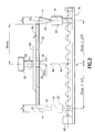
- a plasma jet 10 is produced by plasma jet generator 20 of any known type, which is located in a plasma jet process chamber (not shown).
- the ambient gas pressure of the plasma jet process chamber is maintained at about atmospheric pressure.
- the plasma jet generator 20 is preferably oriented so that the plasma jet 10 is directed upwards, relative to the force of gravity, towards a wafer-like article 30 , such as a silicon wafer, which is held in position on holder 40 .
- the article 30 may be secured to the holder 40 by a vacuum chuck or any other known article holding means.
- Article 30 having a surface to be treated 32 is oriented on the holder 40 such that the surface 32 faces the plasma jet 10 , which as illustrated in Figs.
- the holder 40 is rotated by motor 50 with revolution frequency f.
- the article 30 is positioned on the holder 40 so that the rotation axis Ha of the holder 40 is coincident with the articles's inertial center or rotational axis Wa .
- the revolution frequency f of the article 30 about axis Wa is chosen to be less than the time it takes for the temperature of a point on the surface heated at the beginning of a revolution to cool to the temperature the surface point had just before the beginning of the revolution of the article.
- a gradual heating of every point on the surface 32 of the article 30 is caused by the crossing of the plasma jet over the surface 32 of the article 30 during rotation thereof.
- the plasma jet 10 may be directed at an angle to the article's surface 32 .
- the angle between plasma jet 10 and the surface 32 influences the conditions of plasma flowing along surface 32.
- the angle of the plasma jet 10 directed at the surface 32 of the wafer 30 is 90°, in other words, when the angle of the plasma jet 10 is normal to the surface 32 , the plasma spot or plasma footprint 11 on the surface 32 tends to be symmetrical and the plasma properties within plasma footprint 11 on the surface 32 are more uniform than when the plasma jet is directed at the wafer surface at an angle which is less than 90°.
- the plasma jet 10 is directed at the surface 32 in a normal orientation so as to provide the uniform footprint 11 .
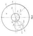
- the plasma jet 10 is moved relative to the surface 32 typically between a first surface point having maximum rotation radius R max and a second wafer surface point having a smaller rotation radius R min .
- Movement of the plasma jet 10 may be done with any trajectory along the surface 32 because only the velocity vector component directed along the wafer rotation radius R is important for realization of this method.
- the relative movement of the plasma jet may be done by supporting the plasma jet on a rail 70 and connecting the generator 20 to a worm gear or screw transmission 80 which is driven by motor 60 .
- the rail 70 is placed parallel to surface 32 and along wafer rotation radius R .
- the plasma jet footprint 11 has limited cross sectional dimension d in the plane of the surface 32, it is convenient to determine the instantaneous position of the plasma jet 10 relative to the surface 32 by the measuring or noting the distance between the article rotation axis Wa and the plasma jet axis Ja.
- the plasma jet 10 starts interacting with the surface 32 at the point of maximum rotation radius R max when it is located at position (R+d/2). Due to the rotation of the motor 60, the plasma jet generator 20 is moved along surface 32 and the plasma jet spot or footprint 11 on the surface 32 is moved towards the article surface points that have a minimal rotation radius, R min .
- the first variant occurs when the rotation axis Wa is located out of the article 30 and at a distance which is more than d/2 from the outer edge 33 of the article 30 , or when the article 30 has an opening 34 with a dimension which is more than plasma jet footprint 11 dimension d and the wafer's rotation axis is located within the opening 34 at a distance which is more than d/2 from its inner edge 36.
- minimal rotation radius R min is more than half the plasma jet's footprint's 11 dimension ( d/2 ).
- Complete treatment of surface 32 is achieved after reaching a distance which is less than R min + d/2 between rotation axis Wa and plasma jet footprint axis Ja .
- the plasma jet 10 When the plasma jet 10 reaches its limit, it may be either turned off or moved further and stopped in the range between 0 and R min - d/2 without incurring damage to the article 30.
- Relative movement velocity v(R) is changed by controlling the frequency of motor 50 having a shaft 55 which is connected to holder 40 to cause holder 40 to rotate.
- the velocity of the plasma jet 10 relative to the article 30 around any rotation radius R is given by 2 ⁇ fR, and is chosen to be greater than the velocity providing the plasma jet shift in the radial direction of the article, v(R).
- the heat input from the plasma jet around the rotation radius spreads in the article material due to heat conductivity for a duration time equal to a revolution, t rev .
- the maximum velocity in the radial direction v max (R) is given by the requirement for uniform treatment, that the plasma jet shift in the radial direction be less than the plasma jet dimension D over the duration of one revolution, t rev .
- the plasma jet foot print 11 on the wafer surface has dimension d, which is about several centimeters and non-uniform distribution of heat flux. That distribution may be measured by calorimeter or any other known means.
- the relative movement velocity function may be found by routine experimental procedure.
- the rotation frequency f is fixed and the article 30 is to be heated from initial temperature To the temperature T w (R) .
- the velocity v(R) is chosen arbitrarily from the range limited by the above mentioned conditions and may be taken as constant.
- one plasma jet pass along the article surface 32 is made.
- the temperature distribution T heat ( R ) along article's radius R is measured.
- This procedure may be extended to a general iterative procedure to obtain an optimal velocity function, v opt ( R ).
- a new velocity function, v i+1 ( R ) can be obtained from the previous velocity function v i ( R ); the measured temperature profile across the wafer, T heat,i ( R ), obtained when executing the velocity function V i ( R ); and the previously measured temperature profile, T heat, i- 1 ( R ), obtained when executing the velocity function v i-1 ( R ):
- v i+1 (R) (T heat, i (R) - T heat, i-1 (R))/T w (R)-T heat, i-1 (R))V i (R)
- the velocity function for this iteration can then be used for the temperature treatment process and is an optimum velocity function, v opt ( R ).
- T d some acceptable temperature difference
- v * opt (R) ((T * w (R) - T 0 )/ T w (R)- T 0 )v opt (R)
- the temperature to which the article should be heated depends on application requirements, for example:
- Plasma jet treatment may be used for thin polymer film removal or polymer photo resist stripping from the article surface.
- the relative movement velocity along article rotation radius is chosen less then velocity providing heating polymer film surface on article surface up to polymer ablation temperature.
- Specific polymer ablation temperature is usually very close to polymer melting temperature and may be obtained from handbooks on polymer properties.
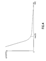
- the v abl ( R ) may be found experimentally by the following procedure. For given inert gas plasma jet parameters, the polymer removal thickness ⁇ h is measured for different values v(R). A typical plot ⁇ h versus v(R) is shown at FIG. 4. The v abl ( R ) is the value where the curve has sharp slope change.
- the velocity v abl (R) is threshold for starting of polymer ablation. All velocity values v(R) ⁇ v abl (R) provide polymer ablation and removal without dependence on whether the plasma jet consists of chemical reactants or not. The smaller v(R) , the greater removal thickness during each pass.
- the relative movement velocity v(R) (v(R) ⁇ V abl (R)) along article rotation radius Wa is changed depending on the distance between plasma jet footprint 11 at the article surface 32 and article rotation axis Wa so that the removal thickness of the polymer at article surface points at all rotation radii be equal to removal thickness at article surface points at the minimum rotation radius.
- the velocity function for the relative movement of the plasma jet relative to the axis of rotation of the article 30 may be determined directly from measured polymer ablation removal by the following steps.
- the velocity v(R) is chosen from the range v(R) ⁇ v abl (R) ; it may be taken as the velocity function that provides uniform heating of the article.
- the velocity v(R) is chosen from the range v(R) ⁇ v abl (R) ; it may be taken as the velocity function that provides uniform heating of the article.
- the velocity v(R) is chosen from the range v(R) ⁇ v abl (R) ; it may be taken as the velocity function that provides uniform heating of the article.
- the polymer thickness removal ⁇ h(R) is measured along the article radius in steps ⁇ r.
- ⁇ h av ( ⁇ r/R max ) ⁇ ⁇ h(R i )
- V des (R) ( ⁇ h des / ⁇ h av )*v opt (R).
- N H/ ⁇ h.
- a reactant which is able to produce volatile chemical substance with the material components is added to plasma jet.
- the reactant may be fluorine containing gas (freon, SF 6 , NF 3 , etc.) for etching Si, poly-Si, SiO 2 , Si 3 N 4 , other Si-based materials, M o , Ti, W, Cr. It may be chlorine containing gas (CCl 4 ) for etching Aluminum. It may be oxygen or hydrogen for etching polymers such as photo resists, or polyimide.
- the relative movement velocity of the plasma jet 10 along the article's rotation radius R is changed depending on the distance between the plasma jet footprint 11 at the article surface 32 and the article rotation axis Wa to provide a removal thickness of wafer surface material at wafer surface points at all rotation radii be equal to removal thickness at the wafer surface point with minimal rotation radius.
- the etch removal rate and etch uniformity are determined by the relative movement velocity function v etch (R) for given plasma jet parameters and reactant concentration.
- the velocity of function v etch (R) may be found by an experimental procedure provided by the following steps.
- the velocity v etch (R) may be taken as the velocity function providing uniform heating of the article.
- one plasma jet pass along through the wafer is made.
- etch removal thickness ⁇ h(R) along article radius is measured in steps ⁇ r.
- the velocity function for relative movement of the plasma jet should be chosen to be more than the ablation threshold velocity for the polymer material to avoid ablation removal of the polymer mask.
- At least one reactant gas which is able to produce a nonvolatile chemical substance on the wafer surface is added to the plasma jet 10.
- adding SiH 4 to the plasma jet 10 allows deposition of amorphous or poly Si if the plasma jet and process chamber ambient gases are inert. If a mixture of SiH 4 or silica organic substance vapor and oxygen is added to the plasma jet, silicon oxide film is deposited onto wafer surface.
- the relative movement velocity v dep (R) along wafer rotation radius is changed depending on distance between plasma jet at the wafer surface and wafer rotation axis to provide a deposited layer thickness at wafer surface points at all rotation radii that is equal to the deposited layer thickness at wafer surface point with minimal rotation radius.
- the velocity function v dep (R) may be found by routine experimental procedure by the following steps.
- the velocity v dep (R) may be taken as velocity providing uniform heating of the wafer.
- one plasma jet pass along through the wafer is made.
- material deposition thickness ⁇ h(R) along wafer radius is measured in increments ⁇ r.
- the average deposition thickness ⁇ h av is calculated as
- the method may be employed for several plasma jet operations. It is to be understood that the embodiments described herein are merely illustrative of the principles of the invention. Various modifications may be made thereto by persons skilled in the art which will embody the principles of the invention and fall within the spirit and scope thereof. Hence, the present invention is deemed limited only by the appended claims and the reasonable interpretation thereof.
Landscapes
- Chemical & Material Sciences (AREA)
- Engineering & Computer Science (AREA)
- Physics & Mathematics (AREA)
- Plasma & Fusion (AREA)
- Chemical Kinetics & Catalysis (AREA)
- General Chemical & Material Sciences (AREA)
- Materials Engineering (AREA)
- Mechanical Engineering (AREA)
- Metallurgy (AREA)
- Organic Chemistry (AREA)
- Analytical Chemistry (AREA)
- Drying Of Semiconductors (AREA)
- Plasma Technology (AREA)
Claims (6)
- Verfahren zum Behandeln der Oberfläche eines Gegenstands mit einem Plasmastrahl, wobei das Verfahren die folgenden Schritte enthält:wobei das Verfahren weiterhin dadurch gekennzeichnet ist,(a) Bereitstellen eines Gegenstandes (30) mit einer zu behandelnden Oberfläche (32),(b) Bereitstellen eines Plasmastrahls (10),(c) daß der Gegenstand um eine Achse (Wa) gedreht wird, wobei die Drehung einen Rotationsradius (R) definiert, der sich von der Achse aus erstreckt,(d) daß die Oberfläche (32) des Gegenstandes in Kontakt mit dem Plasmastrahl (10) gelangt, um eine Plasmastrahl-Auftrefffläche (11) mit einer vorbestimmten Abmessung auf der Oberfläche (32) des Gegenstandes zu bilden, und(e) daß die Plasmastrahl-Auftrefffläche (11) entlang des Rotationsradius (R) in die radiale Richtung entsprechend einem Geschwindigkeitsprofil entlang des Radius so bewegt wird, daß Wärme auf die Oberfläche (32) des Gegenstandes einwirkt, um ein gewünschtes Temperaturverteilungsprofil auf der Oberfläche (32) des Gegenstandes entlang des Rotationsradius (R) zu erhalten.
- Verfahren nach Anspruch 1,
wobei das Verfahren weiterhin die folgenden Schritte enthält:(a) die Temperatur der Oberfläche (32) des Gegenstands wird entlang des Rotationsradius (R) gemessen, um eine gemessene Temperaturverteilung für die Oberfläche (32) des Gegenstandes entlang des Rotationsradius (R) zu erhalten,(b) die gemessene Temperaturverteilung für die Oberfläche (32) des Gegenstandes wird mit einem gewünschten Temperaturverteilungsprofil für die Oberfläche (32) des Gegenstandes entlang des Rotationsradius (R) verglichen,(c) ein zweites Geschwindigkeitsprofil zum Bewegen der Plasmastrahl-Auftrefffläche (11) gegenüber der Oberfläche (32) des Gegenstands entlang des Rotationsradius (R) wird bestimmt, wobei das zweite Geschwindigkeitsprofil das gewünschte Temperaturverteilungsprofil für die Oberfläche (32) des Gegenstands entlang des Rotationsradius (R) liefert, und(d) die Plasmastrahl-Auftrefffläche (11) wird gegenüber der Oberfläche (32) des Gegenstandes entlang des Rotationsradius (R) entsprechend dem zweiten Geschwindigkeitsprofil so bewegt, daß die Oberfläche (32) des Gegenstands erwärmt wird, um das gewünschte Temperaturverteilungsprofil zu erhalten. - Verfahren nach Anspruch 2,
bei dem das zweite Geschwindigkeitsprofil der Plasmastrahl-Auftrefffläche (11) gegenüber der Oberfläche (32) des Gegenstands entlang des Rotationsradius gemäß der Funktion vdes(R) = ((TWärme(R)-T0)/(TW(R)-T0))*v(R) bestimmt wird, wobei vdes(R) die Geschwindigkeit der Plasmastrahl-Auftrefffläche (11) gegenüber der Oberfläche (32) des Gegenstands an einem Punkt auf dem Radius ist, die erforderlich ist, um die Oberfläche (32) des Gegenstands auf eine gewünschte Temperatur zu erwärmen, TWärme(R) die gemessene Temperatur der Oberfläche des Gegenstands an dem Punkt auf dem Radius ist, T0 die Anfangstemperatur der Oberfläche des Gegenstands ist, TW(R) eine gewünschte Temperatur für die Oberfläche des Gegenstands an dem Punkt auf dem Radius ist und v(R) die Anfangsgeschwindigkeit der Plasmastrahl-Auftrefffläche gegenüber der Oberfläche des Gegenstands an einem Punkt auf dem Radius ist. - Verfahren nach Anspruch 3,
bei dem die Temperatur des Gegenstands auf eine gleichmäßige Temperatur im Bereich von ca. 30 °C bis 1200 °C gesteuert wird. - Verfahren zum Behandeln der Oberfläche eines Gegenstands mit einem Plasmastrahl,
wobei das Verfahren die folgenden Schritte enthält:(a) Bereitstellen eines Gegenstandes (30) mit einer zu behandelnden Oberfläche (32),(b) Bereitstellen eines Plasmastrahls (10) zum Abätzen von Material von der Oberfläche des Gegenstands, wobei das Verfahren weiterhin dadurch gekennzeichnet ist,(c) daß der Gegenstand um eine Achse (Wa) gedreht wird, wobei die Drehung einen Rotationsradius (R) definiert, der sich von der Achse aus erstreckt,(d) daß die Oberfläche (32) des Gegenstandes in Kontakt mit dem Plasmastrahl (10) gelangt, um eine Plasmastrahl-Auftrefffläche (11) mit einer vorbestimmten Abmessung auf der Oberfläche (32) des Gegenstands zu bilden,(e) daß die Plasmastrahl-Auftrefffläche (11) gegenüber der Oberfläche des Gegenstandes entlang des Rotationsradius (R) entsprechend einem ersten Geschwindigkeitsprofil so bewegt wird, daß Material von der Oberfläche (32) des Gegenstands abgenommen wird,(f) daß die Dicke des Gegenstandes (30) entlang des Rotationsradius gemessen wird, um eine gemessene Dickenverteilung für den Gegenstand (30) entlang des Rotationsradius (R) zu erhalten,(g) daß die gemessene Dickenverteilung für den Gegenstand (30) mit einem gewünschten Dickenverteilungsprofil für den Gegenstand (30) entlang des Rotationsradius (R) verglichen wird,(h) daß ein zweites Geschwindigkeitsprofil zum Bewegen der Plasmastrahl-Auftrefffläche (11) gegenüber der Oberfläche (32) des Gegenstands entlang des Rotationsradius (R) bestimmt wird, mit welchem das gewünschte Dickenverteilungsprofil für den Gegenstand entlang des Rotationsradius (R) erzielt wird, und(i) daß die Plasmastrahl-Auftrefffläche (11) gegenüber der Oberfläche (32) des Gegenstands entlang des Rotationsradius (R) entsprechend dem zweiten Geschwindigkeitsprofil so bewegt wird, daß Material von der Oberfläche (32) des Gegenstands entfernt wird, um das gewünschte Dickenverteilungsprofil zu erhalten. - Verfahren nach Anspruch 5,
bei dem das zweite Geschwindigkeitsprofil der Plasmastrahl-Auftrefffläche (11) gegenüber der Oberfläche (32) des Gegenstands entlang des Rotationsradius gemäß der Funktion vdes(R) = (Δhdes/Δhsv)*vÄtz(R) bestimmt wird, wobei Vdes(R) die gewünschte Geschwindigkeit der Plasmastrahl-Auftrefffläche (11) gegenüber der Oberfläche (32) des Gegenstands an einem Punkt auf dem Radius (R) ist, die erforderlich ist, um Material von der Oberfläche (32) des Gegenstands zu entfernen, um eine gewünschte Dicke zu erhalten, wobei Δhdes die gewünschte Dicke an dem Punkt auf dem Radius ist, Δhsv die gemessene Durchschnittsdicke ist und vÄtz(R) die Anfangsgeschwindigkeit der Plasmastrahl-Auftrefffläche (11) gegenüber der Oberfläche (32) des Gegenstandes an dem Punkt auf dem Radius ist.
Applications Claiming Priority (3)
| Application Number | Priority Date | Filing Date | Title |
|---|---|---|---|
| US1885696P | 1996-05-31 | 1996-05-31 | |
| US18856P | 1996-05-31 | ||
| PCT/US1997/009069 WO1997045856A1 (en) | 1996-05-31 | 1997-05-28 | Method for treating articles with a plasma jet |
Publications (2)
| Publication Number | Publication Date |
|---|---|
| EP0902961A1 EP0902961A1 (de) | 1999-03-24 |
| EP0902961B1 true EP0902961B1 (de) | 2000-07-05 |
Family
ID=21790104
Family Applications (1)
| Application Number | Title | Priority Date | Filing Date |
|---|---|---|---|
| EP97927804A Expired - Lifetime EP0902961B1 (de) | 1996-05-31 | 1997-05-28 | Verfahren zum behandeln eines scheibens mit einem plasmastrahl |
Country Status (6)
| Country | Link |
|---|---|
| US (1) | US6238587B1 (de) |
| EP (1) | EP0902961B1 (de) |
| JP (1) | JP2000511356A (de) |
| KR (1) | KR20000016136A (de) |
| DE (1) | DE69702452T2 (de) |
| WO (1) | WO1997045856A1 (de) |
Families Citing this family (36)
| Publication number | Priority date | Publication date | Assignee | Title |
|---|---|---|---|---|
| US6882030B2 (en) | 1996-10-29 | 2005-04-19 | Tru-Si Technologies, Inc. | Integrated circuit structures with a conductor formed in a through hole in a semiconductor substrate and protruding from a surface of the substrate |
| JP3537447B2 (ja) | 1996-10-29 | 2004-06-14 | トル‐シ・テクノロジーズ・インコーポレイテッド | 集積回路及びその製造方法 |
| US6498074B2 (en) | 1996-10-29 | 2002-12-24 | Tru-Si Technologies, Inc. | Thinning and dicing of semiconductor wafers using dry etch, and obtaining semiconductor chips with rounded bottom edges and corners |
| US6139678A (en) | 1997-11-20 | 2000-10-31 | Trusi Technologies, Llc | Plasma processing methods and apparatus |
| US6406759B1 (en) | 1998-01-08 | 2002-06-18 | The University Of Tennessee Research Corporation | Remote exposure of workpieces using a recirculated plasma |
| US6168697B1 (en) | 1998-03-10 | 2001-01-02 | Trusi Technologies Llc | Holders suitable to hold articles during processing and article processing methods |
| US6660643B1 (en) * | 1999-03-03 | 2003-12-09 | Rwe Schott Solar, Inc. | Etching of semiconductor wafer edges |
| US6287976B1 (en) | 1999-05-19 | 2001-09-11 | Tru-Si Technologies, Inc. | Plasma processing methods and apparatus |
| DE19925790A1 (de) * | 1999-06-05 | 2000-12-07 | Inst Oberflaechenmodifizierung | Verfahren und Vorrichtung zur Bearbeitung von optischen und anderen Oberflächen mittels Hochrate-Plasmaprozessen |
| EP1246710A4 (de) * | 1999-09-28 | 2007-07-04 | Jetek Inc | Verfahren und vorrichtung unter atmosphärischen bedingungen zum schnellen und kotrolierten entfernen von polymeren aus durch grosse tiefen-weiten-verhältnisszahlen gekennzeichneten löchern |
| US7365019B2 (en) | 1999-11-01 | 2008-04-29 | Jetek, Llc | Atmospheric process and system for controlled and rapid removal of polymers from high aspect ratio holes |
| US6467297B1 (en) | 2000-10-12 | 2002-10-22 | Jetek, Inc. | Wafer holder for rotating and translating wafers |
| US6322903B1 (en) | 1999-12-06 | 2001-11-27 | Tru-Si Technologies, Inc. | Package of integrated circuits and vertical integration |
| US6825101B1 (en) * | 2000-03-27 | 2004-11-30 | Ultratech, Inc. | Methods for annealing a substrate and article produced by such methods |
| KR20010105640A (ko) * | 2000-05-17 | 2001-11-29 | 구자홍 | 평면 브라운관의 새도우 마스크 고정 레일 |
| US6749764B1 (en) | 2000-11-14 | 2004-06-15 | Tru-Si Technologies, Inc. | Plasma processing comprising three rotational motions of an article being processed |
| US7591957B2 (en) * | 2001-01-30 | 2009-09-22 | Rapt Industries, Inc. | Method for atmospheric pressure reactive atom plasma processing for surface modification |
| US7510664B2 (en) | 2001-01-30 | 2009-03-31 | Rapt Industries, Inc. | Apparatus and method for atmospheric pressure reactive atom plasma processing for shaping of damage free surfaces |
| US6717254B2 (en) | 2001-02-22 | 2004-04-06 | Tru-Si Technologies, Inc. | Devices having substrates with opening passing through the substrates and conductors in the openings, and methods of manufacture |
| US6699356B2 (en) * | 2001-08-17 | 2004-03-02 | Applied Materials, Inc. | Method and apparatus for chemical-mechanical jet etching of semiconductor structures |
| US6660177B2 (en) | 2001-11-07 | 2003-12-09 | Rapt Industries Inc. | Apparatus and method for reactive atom plasma processing for material deposition |
| CN1308884C (zh) | 2002-03-20 | 2007-04-04 | 讯宝科技公司 | 应用公共成像阵列的捕像系统和方法 |
| US6908845B2 (en) | 2002-03-28 | 2005-06-21 | Intel Corporation | Integrated circuit die and an electronic assembly having a three-dimensional interconnection scheme |
| US6848177B2 (en) | 2002-03-28 | 2005-02-01 | Intel Corporation | Integrated circuit die and an electronic assembly having a three-dimensional interconnection scheme |
| JP3814558B2 (ja) * | 2002-04-22 | 2006-08-30 | スピードファム株式会社 | 局所ドライエッチング方法及び半導体ウェハ表面の位置−厚さデータの処理方法 |
| US20080017316A1 (en) * | 2002-04-26 | 2008-01-24 | Accretech Usa, Inc. | Clean ignition system for wafer substrate processing |
| US20080190558A1 (en) * | 2002-04-26 | 2008-08-14 | Accretech Usa, Inc. | Wafer processing apparatus and method |
| US20080011332A1 (en) * | 2002-04-26 | 2008-01-17 | Accretech Usa, Inc. | Method and apparatus for cleaning a wafer substrate |
| US7371992B2 (en) | 2003-03-07 | 2008-05-13 | Rapt Industries, Inc. | Method for non-contact cleaning of a surface |
| AT412719B (de) * | 2003-06-16 | 2005-06-27 | Eckelt Glas Gmbh | Verfahren und vorrichtung zum bereichsweisen entschichten von glasscheiben |
| US7304263B2 (en) * | 2003-08-14 | 2007-12-04 | Rapt Industries, Inc. | Systems and methods utilizing an aperture with a reactive atom plasma torch |
| US7297892B2 (en) * | 2003-08-14 | 2007-11-20 | Rapt Industries, Inc. | Systems and methods for laser-assisted plasma processing |
| NL1030896C2 (nl) * | 2006-01-11 | 2007-07-12 | Otb Group Bv | Werkwijze en inrichting voor het gecontroleerd deponeren van materiaal door middel van plasma op een driedimensionaal substraat. |
| US20140134849A1 (en) * | 2012-11-09 | 2014-05-15 | Intermolecular Inc. | Combinatorial Site Isolated Plasma Assisted Deposition |
| CN108700815B (zh) | 2015-12-23 | 2024-03-19 | Asml荷兰有限公司 | 用于去除衬底上的光敏材料的方法 |
| CN113002172B (zh) * | 2021-02-25 | 2022-08-30 | 江西省中子能源有限公司 | 一种锂电池成品壳体喷码烘干系统 |
Family Cites Families (9)
| Publication number | Priority date | Publication date | Assignee | Title |
|---|---|---|---|---|
| US5356672A (en) * | 1990-05-09 | 1994-10-18 | Jet Process Corporation | Method for microwave plasma assisted supersonic gas jet deposition of thin films |
| WO1992012610A1 (fr) | 1990-12-26 | 1992-07-23 | Inzhenerny Tsentr ''plazmodinamika'' | Dispositif de traitement de materiau a l'arc de plasma |
| GB2271124B (en) | 1990-12-26 | 1995-09-27 | Opa | Method and apparatus for plasma treatment of a material |
| RU2030811C1 (ru) | 1991-05-24 | 1995-03-10 | Инженерный центр "Плазмодинамика" | Установка для плазменной обработки твердого тела |
| JPH0570290A (ja) * | 1991-09-11 | 1993-03-23 | Hitachi Chem Co Ltd | ダイヤモンドの気相合成方法及びその装置 |
| RU2000811C1 (ru) | 1991-10-15 | 1993-10-15 | Инженерный центр "Плазмодинамика" | Способ стерилизации и дезинфекции медицинского оборудовани |
| JPH07500635A (ja) | 1991-11-01 | 1995-01-19 | オーピーエー (オーバーシーズ パブリッシャーズ アソシエーション) アムステルダム ベー・ヴェー | ワーク表面加工方法および装置 |
| DE4138541A1 (de) * | 1991-11-23 | 1993-05-27 | Philips Patentverwaltung | Cvd-verfahren zur beschichtung ausgedehnter substrate |
| JP2947036B2 (ja) * | 1993-12-17 | 1999-09-13 | 株式会社デンソー | 気相成長ダイヤモンドの製造装置 |
-
1997
- 1997-05-28 EP EP97927804A patent/EP0902961B1/de not_active Expired - Lifetime
- 1997-05-28 DE DE69702452T patent/DE69702452T2/de not_active Expired - Fee Related
- 1997-05-28 KR KR1019980709704A patent/KR20000016136A/ko not_active Withdrawn
- 1997-05-28 US US09/194,141 patent/US6238587B1/en not_active Expired - Fee Related
- 1997-05-28 JP JP09542905A patent/JP2000511356A/ja active Pending
- 1997-05-28 WO PCT/US1997/009069 patent/WO1997045856A1/en not_active Ceased
Also Published As
| Publication number | Publication date |
|---|---|
| JP2000511356A (ja) | 2000-08-29 |
| EP0902961A1 (de) | 1999-03-24 |
| DE69702452D1 (de) | 2000-08-10 |
| US6238587B1 (en) | 2001-05-29 |
| KR20000016136A (ko) | 2000-03-25 |
| DE69702452T2 (de) | 2000-11-23 |
| WO1997045856A1 (en) | 1997-12-04 |
Similar Documents
| Publication | Publication Date | Title |
|---|---|---|
| EP0902961B1 (de) | Verfahren zum behandeln eines scheibens mit einem plasmastrahl | |
| US11152211B2 (en) | Semiconductor wafer thinning systems and related methods | |
| US5911852A (en) | Plasma processing apparatus | |
| EP0283311B1 (de) | Verfahren zur Herstellung von Dünnschichten | |
| US6221205B1 (en) | Apparatus for improving the performance of a temperature-sensitive etch | |
| JP3329685B2 (ja) | 計測装置および計測方法 | |
| US8945408B2 (en) | Etch process for reducing directed self assembly pattern defectivity | |
| US7745762B2 (en) | Optimizing the thermal budget during a pulsed heating process | |
| TWI570801B (zh) | 用以降低定向自組裝圖樣瑕疵狀態之蝕刻程序 | |
| KR20050004834A (ko) | 튜너블 정전식 척을 위한 가변 온도 처리 | |
| US7892986B2 (en) | Ashing method and apparatus therefor | |
| JPH0263293B2 (de) | ||
| EP0258698A2 (de) | Trockenes Ätzverfahren | |
| KR20030035825A (ko) | 플렉시블 기판상에 반도체 막을 형성하는 장치 | |
| EP0749148B1 (de) | Plasmabearbeitungsgerät | |
| US6955991B2 (en) | Atmospheric process and system for controlled and rapid removal of polymers from high depth to width aspect ratio holes | |
| WO2023219716A1 (en) | Selective and isotropic etch of silicon over silicon-germanium alloys and dielectrics; via new chemistry and surface modification | |
| JPH10214823A (ja) | プラズマ処理装置 | |
| KR100360159B1 (ko) | 다결정실리콘의 제조방법 | |
| JP6318363B2 (ja) | プラズマ処理装置及び方法、電子デバイスの製造方法 | |
| US6221203B1 (en) | Apparatus and method for controlling temperature of a chamber | |
| EP1246710A1 (de) | Verfahren und vorrichtung unter atmosphärischen bedingungen zum schnellen und kotrolierten entfernen von polymeren aus durch grosse tiefen-weiten-verhältnisszahlen gekennzeichneten löchern | |
| WO2015034600A1 (en) | Etch process for reducing directed self assembly pattern defectivity using direct current superpositioning | |
| JPH05234949A (ja) | プラズマ処理装置 | |
| JPH04167523A (ja) | ドライエッチング装置 |
Legal Events
| Date | Code | Title | Description |
|---|---|---|---|
| PUAI | Public reference made under article 153(3) epc to a published international application that has entered the european phase |
Free format text: ORIGINAL CODE: 0009012 |
|
| 17P | Request for examination filed |
Effective date: 19981201 |
|
| AK | Designated contracting states |
Kind code of ref document: A1 Designated state(s): DE FR GB |
|
| GRAG | Despatch of communication of intention to grant |
Free format text: ORIGINAL CODE: EPIDOS AGRA |
|
| RAP1 | Party data changed (applicant data changed or rights of an application transferred) |
Owner name: IPEC PRECISION, INC. |
|
| 17Q | First examination report despatched |
Effective date: 19990826 |
|
| GRAG | Despatch of communication of intention to grant |
Free format text: ORIGINAL CODE: EPIDOS AGRA |
|
| GRAH | Despatch of communication of intention to grant a patent |
Free format text: ORIGINAL CODE: EPIDOS IGRA |
|
| GRAH | Despatch of communication of intention to grant a patent |
Free format text: ORIGINAL CODE: EPIDOS IGRA |
|
| GRAA | (expected) grant |
Free format text: ORIGINAL CODE: 0009210 |
|
| AK | Designated contracting states |
Kind code of ref document: B1 Designated state(s): DE FR GB |
|
| REF | Corresponds to: |
Ref document number: 69702452 Country of ref document: DE Date of ref document: 20000810 |
|
| ET | Fr: translation filed | ||
| PGFP | Annual fee paid to national office [announced via postgrant information from national office to epo] |
Ref country code: FR Payment date: 20010501 Year of fee payment: 5 |
|
| PGFP | Annual fee paid to national office [announced via postgrant information from national office to epo] |
Ref country code: GB Payment date: 20010504 Year of fee payment: 5 |
|
| PLBE | No opposition filed within time limit |
Free format text: ORIGINAL CODE: 0009261 |
|
| STAA | Information on the status of an ep patent application or granted ep patent |
Free format text: STATUS: NO OPPOSITION FILED WITHIN TIME LIMIT |
|
| PGFP | Annual fee paid to national office [announced via postgrant information from national office to epo] |
Ref country code: DE Payment date: 20010508 Year of fee payment: 5 |
|
| 26N | No opposition filed | ||
| REG | Reference to a national code |
Ref country code: GB Ref legal event code: IF02 |
|
| PG25 | Lapsed in a contracting state [announced via postgrant information from national office to epo] |
Ref country code: GB Free format text: LAPSE BECAUSE OF NON-PAYMENT OF DUE FEES Effective date: 20020528 |
|
| PG25 | Lapsed in a contracting state [announced via postgrant information from national office to epo] |
Ref country code: DE Free format text: LAPSE BECAUSE OF NON-PAYMENT OF DUE FEES Effective date: 20021203 |
|
| GBPC | Gb: european patent ceased through non-payment of renewal fee |
Effective date: 20020528 |
|
| PG25 | Lapsed in a contracting state [announced via postgrant information from national office to epo] |
Ref country code: FR Free format text: LAPSE BECAUSE OF NON-PAYMENT OF DUE FEES Effective date: 20030131 |
|
| REG | Reference to a national code |
Ref country code: FR Ref legal event code: ST |