EP0902500A2 - Flache Bildanzeigevorrichtung - Google Patents
Flache Bildanzeigevorrichtung Download PDFInfo
- Publication number
- EP0902500A2 EP0902500A2 EP98307316A EP98307316A EP0902500A2 EP 0902500 A2 EP0902500 A2 EP 0902500A2 EP 98307316 A EP98307316 A EP 98307316A EP 98307316 A EP98307316 A EP 98307316A EP 0902500 A2 EP0902500 A2 EP 0902500A2
- Authority
- EP
- European Patent Office
- Prior art keywords
- article
- support film
- conductor
- adhesive
- signal transmission
- Prior art date
- Legal status (The legal status is an assumption and is not a legal conclusion. Google has not performed a legal analysis and makes no representation as to the accuracy of the status listed.)
- Withdrawn
Links
Images




Classifications
-
- H—ELECTRICITY
- H01—ELECTRIC ELEMENTS
- H01R—ELECTRICALLY-CONDUCTIVE CONNECTIONS; STRUCTURAL ASSOCIATIONS OF A PLURALITY OF MUTUALLY-INSULATED ELECTRICAL CONNECTING ELEMENTS; COUPLING DEVICES; CURRENT COLLECTORS
- H01R4/00—Electrically-conductive connections between two or more conductive members in direct contact, i.e. touching one another; Means for effecting or maintaining such contact; Electrically-conductive connections having two or more spaced connecting locations for conductors and using contact members penetrating insulation
- H01R4/04—Electrically-conductive connections between two or more conductive members in direct contact, i.e. touching one another; Means for effecting or maintaining such contact; Electrically-conductive connections having two or more spaced connecting locations for conductors and using contact members penetrating insulation using electrically conductive adhesives
-
- H—ELECTRICITY
- H01—ELECTRIC ELEMENTS
- H01R—ELECTRICALLY-CONDUCTIVE CONNECTIONS; STRUCTURAL ASSOCIATIONS OF A PLURALITY OF MUTUALLY-INSULATED ELECTRICAL CONNECTING ELEMENTS; COUPLING DEVICES; CURRENT COLLECTORS
- H01R12/00—Structural associations of a plurality of mutually-insulated electrical connecting elements, specially adapted for printed circuits, e.g. printed circuit boards [PCB], flat or ribbon cables, or like generally planar structures, e.g. terminal strips, terminal blocks; Coupling devices specially adapted for printed circuits, flat or ribbon cables, or like generally planar structures; Terminals specially adapted for contact with, or insertion into, printed circuits, flat or ribbon cables, or like generally planar structures
- H01R12/70—Coupling devices
- H01R12/7076—Coupling devices for connection between PCB and component, e.g. display
Definitions
- This invention generally relates to a planar display apparatus, and more particularly to an improved electrical interconnect for electrically coupling a planar display apparatus to electronic driver circuitry.
- CRT cathode ray tube or CRT
- U.S. Patent No. 5,577,944 to Taylor CRTs are of limited use for laptop or portable computers, for example, in that they require a significant amount of depth and are relatively fragile and heavy. Since planar or flat panel displays, as their name implies, are relatively narrow in depth, and have comparable display characteristics to that of CRTs, a considerable amount of interest in these displays has developed over the past few years.
- a conventionally designed flat panel display includes a substrate such as a glass plate having a plurality of row and column conductors etched upon the plate. Each of the row conductors and column conductors extend to the periphery of the plate for connection to driver circuitry which is selectively energized to form patterns on a display area in accordance with data to be displayed.
- driver circuitry is in the form of integrated circuits that are employed to drive a designated group of conductors from the periphery of the column and row.
- a typical driver circuit is capable of driving individual conductors where the driver circuit receives inputs provided by the electronics external to the panel.
- ACF anisotropic conductive film
- the flex circuit is terminated to the display glass plate by applying heat and pressure to the ACF which is sandwiched between the flex circuit and the display glass plate. This process results in the formation of a conductive path from the conductive traces on the underside of the flex circuit through the ACF to the conductive traces on the top surface of the display substrate (e.g. glass plate).
- the ACF also creates a mechanical bond between the flex circuit and the display glass.
- Flex circuit/ACF bonding does include several drawbacks.
- known ACF materials have limited operating temperatures.
- many applications for flat panel displays require use and/or storage in environments having temperatures exceeding the operating temperature limits of readily-available materials.
- liquid crystal display material has been the temperature limitation, but newer display technologies, such as a field emission display (“FED”) enable storage or use in temperatures higher than the operating temperatures of readily-available ACFs.
- FED field emission display
- the flex circuit /ACF interconnect is the limiting element in enabling the display to be used or stored in high temperature environments.
- ACF flex circuit/ACF interconnects
- ACF requires a minimum border width of typically about 1.5 mm for termination, due to the need for adequate contact area to compensate for the high contact resistance per unit contact area between the flex circuit and the ACF and again between the ACF and the display substrate.
- a reduced border width is possible only if the pitch of the pads is increased.
- ACF requires a termination circuit board which is connected to the driver die or chip package; that is, neither the ACF nor the interconnect can be directly connected to the driver die, In fact, no other interconnect method presently available allows for direct attachment of the interconnect to a driver die. Direct die termination eliminates one level of packaging in the assembly process, thereby resulting in cost savings and reliability improvements.
- the driver die can be mounted directly onto the glass periphery.
- the connection of the driver die to the glass can be achieved by any suitable conventional method.
- a major disadvantage with this technology is that increased border area is required to mount the die.
- This application has also been known to be difficult to rework and can result in discarded displays.
- Heat sealing has also been used to interconnect the driver to the glass plate; however, while heat sealing has the advantage of being able to withstand higher temperatures than ACF, it has a pitch limitation of at least 120 microns, well above the 70 microns or less required for most displays.
- an article comprises a flat panel display unit having a plurality of electrically conductive lead pads which are disposed on a surface thereof.
- the article further comprises a microminiature planar signal transmission cable having opposed first and second ends. The first end of the cable is electrically connected to a selected number of the electrically conductive lead pads.
- the cable also has at least one support film having opposite first and second surfaces, and a thickness of less than about 0.003 inch.
- At least one layer of adhesive is disposed on the first surface of the support film, the adhesive having a thickness of less than about 0.001 inch.
- At least one preformed signal transmission conductor, having a widthwise dimension of less than about 0.002 inch, is embedded within the layer of adhesive.
- the article also comprises means for electrically controlling the flat panel display electrically connected to the second end of the cable.
- an object of the present invention to provide an article comprising a display panel, driver electronic circuitry, and an interconnect therebetween that can be wire-bondably terminated to low temperature plastic substrates at room temperature by means of an ultrasonic process.
- Another object of the present invention is that of an article which permits higher maximum storage and/or use temperatures than prior art interconnects.
- Yet another object of the present invention is that of an article which permits reduced border area around the periphery of the display area.
- a further object of the present invention is that of an article which can be connected directly to the driver die, thus eliminating at least one packaging step.
- Yet a further object of the present invention is that of an article which is less expensive to produce in high-volume production than other articles, and which is less time consuming to manufacture and install than the other prior art interconnects.
- a microminiature planar signal transmission cable of the present invention is generally illustrated at 10 in Figures 1 and 2.
- the cable 10 comprises three principal . components, namely, a support film 12, a layer of adhesive 14 applied on the support film, and a plurality of conductors 16 attached to the layer of adhesive.
- the cable 10 can have any number of support films 12 and adhesive layers 14, as required for strength and rigidity, and still fall within the scope of the present invention.
- the cable 10 can be fabricated with any number of conductors 16 as well.
- the support film 12 includes an upwardly facing (first) surface 18 and an opposite, downwardly facing (second) surface 20. As shown in Figure 2, the upwardly facing surface 18 has the layer of adhesive 14 disposed thereon.
- the support film 12 of the cable 10 is fabricated from any suitable polymeric material, such as polyimide, for example. (This material is sold commercially on spools or reels, and can be purchased from UBE Industries, Ltd., under the registered trademark UPILEX.)
- the support film 12 gives the cable 10 its required strength and rigidity.
- the support film 12 has a thickness of less than about 0.003 inch.
- the support film 12 can also be fabricated from polyester, or a fluoropolymer, such as porous polytetrafluoroethylene, polytetrafluoroethylene, fluorinated ethylenepropylene, or perfluoroalkoxy polymer.
- a fluoropolymer such as porous polytetrafluoroethylene, polytetrafluoroethylene, fluorinated ethylenepropylene, or perfluoroalkoxy polymer.
- porous polytetrafluoroethylene PTFE
- PTFE porous polytetrafluoroethylene
- the porous PTFE is a porous expanded polytetrafluoroethylene membrane having a microstructure of interconnected nodes and fibrils, as described in U.S. Patent Nos. 3,953,566 and 4,187,390, which are incorporated herein by reference, and which fully describe the preferred materials and processes for making them.
- the layer of adhesive 14 is applied onto the first surface 18 of the support film by any suitable apparatus. It is somewhat important that the layer of adhesive 14 have a uniform thickness and density since voids in the layer can cause inadequate bonding of the conductors 16 to the support film 12.
- the layer of adhesive 14 is a cross-linked, blended polyester polymer.
- the layer of adhesive 14 preferably has a thickness of less than 0.001 inch.
- One preferred method of applying the layer of adhesive 14 to the support film 12 is by adding a solvent to the adhesive which results in it being liquified, and applying the liquified adhesive/solvent mix to the first surface 18 of the support film. After applying the mix, the support film 12 is then dried (either by air or mechanically), thereby dissolving the solvent. This results in the layer of adhesive 14 which can then be manipulated by a doctor blade, or some other similar apparatus, for evening out the layer. During this application process, the support film 12 is removed from its spool or reel and rewound onto another spool after the layer of adhesive 14 has cured.
- the preformed conductors may be any suitable shape and define a width dimension of less than about 0.002 inch. Cylindrically-shaped conductors are typically used and respond well to ultrasonic bonding. Rectangularly-shaped conductors can also be utilized.
- the conductors 16 are fabricated from metal, such as gold, aluminum, gold plated copper, aluminum with silicon, copper, aluminum, aluminum magnesium alloy and tungsten, so that bonding between the conductors and flat metallic pads is enabled by conventional bonding methods. If more than one conductor 16 is required, the conductors are disposed in parallel, co-planar relation at spaced-apart, predetermined intervals. Typically the conductors 16 are spaced at intervals ranging from about 0.0015 inch to about 0.0100 inch.
- the conductor 16 material selection is based on a number of criteria, the most important of which is compatibility with the material to which it is terminated.
- One combination that has been used is aluminum doped with one percent silicon, which is manufactured by American Fine Wire. Conductors 16 fabricated from this material are effectively terminated to molybdenum dioxide pads (or "traces"). Other factors that influence conductor material selection include yield strength, hardness, conductivity and elongation.
- the conductor 16 can further be pre-insulated or bare. If they are pre-insulated, the insulation may be removed or bonded through with ultrasonic methods. If the insulation is removed, the preferred method is with an excimer laser because of its high precision and ability to completely remove the insulation from the conductor.
- the conductors 16 are embedded within the layer of adhesive 14 by any suitable method that employs either force or temperature.
- the conductors 16 are aligned and spaced-apart to the desired configuration, and preferably passed through a nip point (as through rollers) where temperature can also be applied to ensure proper bonding between the support film 12 and the conductors 16. After securing the conductors 16 to the support film 12, the cable 10 is cooled and collected in any well-known fashion.
- the individual conductors 16 may be insulated with a layer (not shown) of suitable insulation material, such as, for example, polyurethane, polyimide, porous polytetrafluoroethylene, polytetrafluoroethylene, or fluorinated ethylenepropylene.
- suitable insulation material such as, for example, polyurethane, polyimide, porous polytetrafluoroethylene, polytetrafluoroethylene, or fluorinated ethylenepropylene.
- the individual conductors 16 may be individually insulated by conventional methods, such as by extrusion, tape wrapping, or dip coating, for example. It is also anticipated that a material may be employed for the conductor insulation which has a higher melt temperature than the material used for the support film 12 to facilitate processing in certain instances.
- ground planes may be included in any embodiment of the present invention.
- Suitable ground plane material may be metal foil or another conductive material.
- Specific embodiments of the present invention are many, so long as the thicknesses of the support film 12 and layer of adhesive 14 are less than 0.003 inch and 0.001 inch, respectively.
- one or more support film(s) 12 can be used. Each support film 12 must be approximately the width of the finished cable 10, or wider.
- one or more adhesive layers 14 may be used eitber as free films and/or as coatings on one or more of the support films 12.
- Tooling to construct the cable 10 of the present invention consists of machined drums and/or rollers, such that the cable components (e.g., support film 12, adhesive layer 14 and conductors 16 described above are formed together, by a continuous process, under heat and/or pressure. Conductors 16 and/or support films 12 can be guided so that their positions with respect to each other are controlled. Tooling may be machined so as to hold each conductor 16 in position. Tooling may also be heated, and/or heat may be applied to some or all of the cable components before they enter the tooling. Process temperatures and the time at which the components are held at elevated temperature are chosen such that the conductors 16 are embedded into the adhesive layer 14.
- Process temperatures and the time at which the components are held at elevated temperature are chosen such that the conductors 16 are embedded into the adhesive layer 14.
- the cable 10 of the present invention may be prepared for termination by having a portion of the support film 12 near one end or both ends removed prior to the conductor embedding process (e.g., by laser stripping). This will allow the free multi-axis movement of the cable 10 for routing onto termination pads, for example.
- the flat panel display device may be any embodiment, such as a liquid crystal display, a field emission display or a CMOS type display, for example.
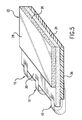
- flat panel display device 22 has a cathode plate 24, an anode plate 26 and a display area 28. As shown in Figure 3, surrounding the display area 28 is a border 30 of sufficient width to accommodate the connection of transmission cables 10 thereto.
- the cathode plate 24 of the display device 22 has a plurality of lead pads or traces, each indicated at 32.
- the lead pads 32 are fabricated from metallic material suitable for electrically bonding to the conductors 16 of the cable 10.
- a preferred method of bonding the conductors 16 of the cable to the metalized lead pads 32 is ultrasonic bonding.
- Anisotropic conductive film (“ACF”) can also be used to bond the materials to one another.
- ACF bonding consists of placing a conductive particle-filled material (e.g., ACF film, liquid or paste) between the conductors 16 and lead pads 32.
- a heated tool is forced down onto the cable 10 such that heat and pressure create an electrical contact between the conductors 16, conductive ACF particles, and the lead pads 32.
- the conductors 16 can also be bonded to the lead pads 32 by cold termination when the cathode plate 24 is fabricated from polymeric material, which is incapable of withstanding high temperatures. Cold termination methods are also well known in the art.
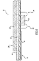
- the transmission cable 10 connects driver circuitry 34, e.g., a display driver, to the cathode plate 24.
- driver circuitry 34 is mounted on the underside of a printed wiring board 36 which is laminated to the underside of . the cathode plate 24.
- At least one bonding wire 38 electrically interconnects the transmission cable 10 to the driver circuitry 34.
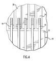
- the microminiature nature of the cable 10 enables it to electrically interconnect the conductors 16 to the lead pads 32 ( Figure 4) for reducing the overall border area 30 of the display device 22.
- the transmission cable 10 is connected directly to the driver circuitry 34. This is another advantage associated with using the transmission cable 10 of the present invention.
- the transmission cable 10 is electrically connected to a semi-conductor device, such as a video display driver die 40, for example.
- a display panel 42 is mounted upon driver die 40.
Landscapes
- Devices For Indicating Variable Information By Combining Individual Elements (AREA)
- Multi-Conductor Connections (AREA)
- Coupling Device And Connection With Printed Circuit (AREA)
- Insulated Conductors (AREA)
- Liquid Crystal (AREA)
Applications Claiming Priority (2)
| Application Number | Priority Date | Filing Date | Title |
|---|---|---|---|
| US927984 | 1992-08-11 | ||
| US92798497A | 1997-09-11 | 1997-09-11 |
Publications (2)
| Publication Number | Publication Date |
|---|---|
| EP0902500A2 true EP0902500A2 (de) | 1999-03-17 |
| EP0902500A3 EP0902500A3 (de) | 2000-11-29 |
Family
ID=25455536
Family Applications (1)
| Application Number | Title | Priority Date | Filing Date |
|---|---|---|---|
| EP98307316A Withdrawn EP0902500A3 (de) | 1997-09-11 | 1998-09-10 | Flache Bildanzeigevorrichtung |
Country Status (3)
| Country | Link |
|---|---|
| EP (1) | EP0902500A3 (de) |
| JP (1) | JPH11167352A (de) |
| KR (1) | KR19990029275A (de) |
Cited By (6)
| Publication number | Priority date | Publication date | Assignee | Title |
|---|---|---|---|---|
| EP1734615A1 (de) * | 2005-06-13 | 2006-12-20 | Research In Motion Limited | Elektrischer Verbinder und elektrisches System für ein Bauteil in einem elektronischen Gerät |
| US7160587B2 (en) * | 2003-08-20 | 2007-01-09 | Tosoh Corporation | Plastic substrate for display and display element |
| US7408786B2 (en) | 2005-06-13 | 2008-08-05 | Research In Motion Limited | Electrical connector and system for a component in an electronic device |
| EP2027760A2 (de) * | 2006-05-22 | 2009-02-25 | Philips Intellectual Property & Standards GmbH | Verbindungsanordnung und verfahren zur verbindung eines hochstromkabels mit einem metalldünnfilm |
| CN104167234A (zh) * | 2014-08-29 | 2014-11-26 | 孙金福 | 一种铜包铝镁合金线 |
| CN110911453A (zh) * | 2018-09-18 | 2020-03-24 | 三星显示有限公司 | 显示装置及其制造方法 |
Families Citing this family (1)
| Publication number | Priority date | Publication date | Assignee | Title |
|---|---|---|---|---|
| KR100696629B1 (ko) * | 2005-09-26 | 2007-03-19 | 삼성에스디아이 주식회사 | 플라즈마 디스플레이 장치 |
Family Cites Families (4)
| Publication number | Priority date | Publication date | Assignee | Title |
|---|---|---|---|---|
| JPS6377284U (de) * | 1986-11-10 | 1988-05-23 | ||
| US5424605A (en) * | 1992-04-10 | 1995-06-13 | Silicon Video Corporation | Self supporting flat video display |
| DE4327099A1 (de) * | 1993-08-12 | 1995-02-16 | Sican Gmbh | Kupplungselement zur Verbindung von auf Folie geführten Mikrostreifenleitungen |
| JP3143565B2 (ja) * | 1994-02-28 | 2001-03-07 | キヤノン株式会社 | フレキシブルプリント配線、その接続装置、及び電気回路装置 |
-
1998
- 1998-08-06 KR KR1019980031968A patent/KR19990029275A/ko not_active Withdrawn
- 1998-09-09 JP JP10255520A patent/JPH11167352A/ja active Pending
- 1998-09-10 EP EP98307316A patent/EP0902500A3/de not_active Withdrawn
Cited By (8)
| Publication number | Priority date | Publication date | Assignee | Title |
|---|---|---|---|---|
| US7160587B2 (en) * | 2003-08-20 | 2007-01-09 | Tosoh Corporation | Plastic substrate for display and display element |
| EP1734615A1 (de) * | 2005-06-13 | 2006-12-20 | Research In Motion Limited | Elektrischer Verbinder und elektrisches System für ein Bauteil in einem elektronischen Gerät |
| US7408786B2 (en) | 2005-06-13 | 2008-08-05 | Research In Motion Limited | Electrical connector and system for a component in an electronic device |
| US7684212B2 (en) | 2005-06-13 | 2010-03-23 | Research In Motion Limited | Electrical connector and system for a component in an electronic device |
| EP2027760A2 (de) * | 2006-05-22 | 2009-02-25 | Philips Intellectual Property & Standards GmbH | Verbindungsanordnung und verfahren zur verbindung eines hochstromkabels mit einem metalldünnfilm |
| CN104167234A (zh) * | 2014-08-29 | 2014-11-26 | 孙金福 | 一种铜包铝镁合金线 |
| CN110911453A (zh) * | 2018-09-18 | 2020-03-24 | 三星显示有限公司 | 显示装置及其制造方法 |
| US12069910B2 (en) | 2018-09-18 | 2024-08-20 | Samsung Display Co., Ltd. | Display device and manufacturing method of display device |
Also Published As
| Publication number | Publication date |
|---|---|
| EP0902500A3 (de) | 2000-11-29 |
| JPH11167352A (ja) | 1999-06-22 |
| KR19990029275A (ko) | 1999-04-26 |
Similar Documents
| Publication | Publication Date | Title |
|---|---|---|
| US5354392A (en) | Method for connecting a wiring arranged on a sheet with another wiring arranged on another sheet by ultrasonic waves | |
| US20100065320A1 (en) | Wiring board and method for manufacturing the same | |
| US5799392A (en) | Method of manufacturing a connecting structure of printed wiring boards | |
| EP2151862A1 (de) | Halbleitervorrichtung und herstellungsverfahren dafür sowie display und herstellungsverfahren dafür | |
| US9860982B1 (en) | Electrical connection of electrical wires to flexible conductive elements | |
| US20200335429A1 (en) | Flexible printed circuit board and method of manufacturing flexible printed circuit board | |
| JP2000269632A (ja) | シールドフレキシブルプリント配線板の製造方法、シールドフレキシブルプリント配線板用補強シールドフィルム及びシールドフレキシブルプリント配線板 | |
| EP0902500A2 (de) | Flache Bildanzeigevorrichtung | |
| EP1928218A1 (de) | Flexible gedruckte leiterplatte und verfahren zu dessen herstellung | |
| JPH09161551A (ja) | 小縁フラットケーブル | |
| EP0675673A2 (de) | Verstärkung für flexible Leiterplatte und verstärkte flexible Leiterplatte | |
| WO1998018138A1 (en) | Microminiature planar signal transmission cable | |
| EP0751700A2 (de) | Kupferkaschiertes Laminat, Verfahren zu dessen Herstellung, Leiterplatte und Verfahren zu deren Herstellung | |
| KR100406090B1 (ko) | 이방성 도전 필름 | |
| CN108243568A (zh) | 可挠性电路板的制作方法 | |
| JP2008192789A (ja) | 成形加工用回路基板、および、これを成形加工して得られる立体回路基板 | |
| CN110521292A (zh) | 印刷电路板及其制造方法 | |
| JP2001313448A (ja) | 両面フレキシブル配線板、icカードおよび両面フレキシブル配線板の製造方法 | |
| JP2011077126A (ja) | 配線板、配線板の製造方法、配線板の接続構造及び配線板の接続方法 | |
| JP2785832B2 (ja) | 半導体装置の実装構造 | |
| JPH0143474B2 (de) | ||
| JP3612848B2 (ja) | フラットケーブルおよびその製造方法 | |
| JPH01194209A (ja) | 熱接着性可撓性配線部材 | |
| US6488198B1 (en) | Wire bonding method and apparatus | |
| JP2002252450A (ja) | カバーレイフィルム |
Legal Events
| Date | Code | Title | Description |
|---|---|---|---|
| PUAI | Public reference made under article 153(3) epc to a published international application that has entered the european phase |
Free format text: ORIGINAL CODE: 0009012 |
|
| AK | Designated contracting states |
Kind code of ref document: A2 Designated state(s): AT BE CH CY DE DK ES FI FR GB GR IE IT LI LU MC NL PT SE |
|
| AX | Request for extension of the european patent |
Free format text: AL;LT;LV;MK;RO;SI |
|
| PUAL | Search report despatched |
Free format text: ORIGINAL CODE: 0009013 |
|
| AK | Designated contracting states |
Kind code of ref document: A3 Designated state(s): AT BE CH CY DE DK ES FI FR GB GR IE IT LI LU MC NL PT SE |
|
| AX | Request for extension of the european patent |
Free format text: AL;LT;LV;MK;RO;SI |
|
| AKX | Designation fees paid | ||
| REG | Reference to a national code |
Ref country code: DE Ref legal event code: 8566 |
|
| STAA | Information on the status of an ep patent application or granted ep patent |
Free format text: STATUS: THE APPLICATION IS DEEMED TO BE WITHDRAWN |
|
| 18D | Application deemed to be withdrawn |
Effective date: 20010331 |