EP0901227A1 - Circuit à retard variable - Google Patents
Circuit à retard variable Download PDFInfo
- Publication number
- EP0901227A1 EP0901227A1 EP98402152A EP98402152A EP0901227A1 EP 0901227 A1 EP0901227 A1 EP 0901227A1 EP 98402152 A EP98402152 A EP 98402152A EP 98402152 A EP98402152 A EP 98402152A EP 0901227 A1 EP0901227 A1 EP 0901227A1
- Authority
- EP
- European Patent Office
- Prior art keywords
- delay
- circuit
- signal
- signals
- combination
- Prior art date
- Legal status (The legal status is an assumption and is not a legal conclusion. Google has not performed a legal analysis and makes no representation as to the accuracy of the status listed.)
- Granted
Links
Images


Classifications
-
- H—ELECTRICITY
- H03—ELECTRONIC CIRCUITRY
- H03K—PULSE TECHNIQUE
- H03K5/00—Manipulating of pulses not covered by one of the other main groups of this subclass
- H03K5/13—Arrangements having a single output and transforming input signals into pulses delivered at desired time intervals
- H03K5/133—Arrangements having a single output and transforming input signals into pulses delivered at desired time intervals using a chain of active delay devices
Definitions
- the invention relates to delay circuits. variable, the delay being adjustable according to a delay setpoint.
- the delay setpoint can take the form of a numerical quantity.
- variable delay circuits are numerous. These delay circuits are for example used for phase adjustments between two logic signals. In this case, one of the two signals is applied to the input of a delay circuit. Adjustment delay of the delay circuit is then controlled by the measurement of the phase shift to compensate between these two signals logical.
- Phase control can be performed at by means of an analog or digital adjustment signal.
- the digital solution is often preferred because it is less sensitive to disturbances and attenuations due to signal transmission.
- it is less sensitive to manufacturing dispersions.
- a first known solution for achieving a digitally controlled delay circuit consists of use a set of basic doors.
- the set of doors is associated with an interconnection system, controlled digitally, and allowing cascade connection of a variable number of elementary doors.
- the application of this type of circuit is however limited to cases where it is not necessary to obtain delay adjustment accuracy less than the delay intrinsic to the elementary door.
- Another known solution is to use a resistance-capacity type circuit where resistance is made up of several elementary resistances, selectively connected in parallel according to the numerical control.
- the delay is fixed by the time constant of the circuit. If all elementary resistors have the same value, the delay obtained is then inversely proportional to the number of selected resistors. Now, to get a constant setting accuracy over the entire range of setting, it is necessary that the function linking the delay to the digital adjustment quantity approaches more of a linear function possible.
- the delay circuit is intended to be used in a circuit locked in phase of type described in the published European patent application under number 0 441 684, filed on January 30, 1991 and entitled "Circuit locked in phase and multiplier of frequency resulting ", the previous solution is not not satisfactory because of its size and its sensitivity to manufacturing dispersions.
- the object of the invention is to propose a circuit to delay allowing precise adjustment, while ensuring with sufficient approximation a linear response delay according to the delay setpoint, on a important time interval, in order to approach with constant adjustment precision.
- the circuit of this patent relates to a circuit with delay to provide an output signal with a delay relative to an input signal.
- the delay is adjustable according to a delay setpoint.
- the delay circuit includes a primary circuit, a combination circuit and a shaping circuit.
- the primary circuit receives the input signal and provides two intermediate signals between them a fixed delay.
- the combination circuit has two inputs and has a command input receiving a control quantity representative of the setpoint.
- the circuit of combination outputs a combination signal resulting from an overlay with a weighting and an integration effect of intermediate signals applied to its inputs.
- Weighting consists of weight each of the signals at the input of the combination circuit.
- the weights values are a function of the order quantity.
- the combination signal supplied by the combination is applied to the input of the bet circuit in shape.
- the shaping circuit has an effect threshold.
- the shaping circuit produces a signal trigger, the output signal, when the combination signal reached by integration effect a determined threshold.
- the effective delay of the output signal by relation to the input signal is dependent on the level of combination signal. It is desirable that maximum and minimum amplitudes of the combination signal are independent of the delay setpoint. In this goal, the sum of the two weights is constant.
- integration into the combination is produced by an integrator or a time constant circuit always presenting a saturation effect defining the extreme levels of combination signal.
- a transition time is defined as the time interval during which the signal combination varies according to a linear function or quasi-linear when one of the coefficients of weighting associated with the intermediate signals is no.
- the combination circuit and / or the fixed delay primary circuit may be dimensioned so that the fixed delay is equal halfway through the transition time.
- the multiplexer we selects, as intermediate signals, signal pairs with a fixed delay between them (as before) and, together, a basic delay by relative to the input signal. In this case, at the time of range jump, there are discontinuities delay technology. If the discontinuity is negative, it creates an impossibility for the enslavement of finding a balanced setting at a acceptable value. In the invention, this is remedied problem by modifying the combination circuit of way, in practice, that it does not allow to explore a whole beach.
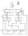
- the delay circuit according to the invention is shown schematically in Figure 1. It includes a primary circuit D1 with fixed delay.
- the D1 circuit receives the input signal e0 and outputs first and second intermediate signals m0 and ml.
- the signals m0 and m1 have between them a fixed delay T.
- the signals m0 and m1 are applied respectively to the inputs X and Y of a combination circuit C providing at output a combination signal f K.
- the combination circuit C comprises a control input CD receiving a command K representative of the weighting coefficients of the combination carried out by the circuit C.
- This command K is a function of a delay setpoint CN.
- the combination signal f K is applied to the input of a shaping circuit F whose output provides the output signal s K.
- a shaping circuit F whose output provides the output signal s K.
- the signal e0 arrives at the input E of the circuit on a first buffer memory (buffer in English literature) T1.
- a first buffer memory buffer in English literature
- three identical buffer memories T1, T2 and T3 are connected in series. They are used to introduce fixed delays to the e0 signal in series. Preferably the fixed delays are all equal to each other so that the signal e0 is delayed by T, 2T, 3T, etc. But the delays could be different from each other.
- the input of the first buffer memory is connected to one of the two inputs of a first MUX0 multiplexer.
- the output of the buffer memory T2 constitutes the other input of the multiplexer MUX0.
- the outputs of the buffer memories T1 and T3 are connected to the two inputs of a second multiplexer MUX1.
- the outputs of the multiplexers MUX0 and MUX1 are connected to the inputs of the combination circuit C performing delay interpolation.
- the output of the combination circuit leads the signal f K to the shaping circuit F.
- the combination circuit consists of two modules U0 and U1. Interpolation can thus be performed between either the signals e0 and r1, or the signals r2 and r1, or the signals r2 and r3. These three combinations are the only ones to have a constant delay equal to T between the signals.
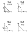
- the curves presented in FIGS. 2 to 9 make it possible to explain the operation of the circuit of FIG. 1. They explain the reasons which prevented the introduction of a simple circuit D1 with fixed delay equal to a time T 'greater than T which would have directly enlarged the delay range. They expose on the one hand the nature of the combination signals f K and of the output signals s K according to the comparison between the fixed delay time T between the signals m0 and m1 and a transition time tm.
- the transition time tm is the duration presented by the combination circuit for passing the signal Fk from its minimum value to its saturation value when K is 0 or 1.
- the figures show the variations of the delay t K in function of the coefficient K for different values of the transition time tm, the fixed delay T being assumed to be fixed.
- the timing diagram in FIG. 2a represents the signals m0 and m1 applied to the inputs X and Y of the circuit combination C.
- the signal m0 being a logic signal, it presents a steep transition front between a first and second level which is followed much more late from another unrepresented front restoring the signal at its first level.
- the falling front represents the end of the pulse of signal R0 which seeks to delay.
- the duration of this pulse is large compared to T, 2T, 3T ....
- the delayed signal m1 has been represented as a signal identical to m0 but delayed by a delay T defined by circuit D1. In practical, the edge of the signal m0 is used by the combination circuit at the moment when the signal m0 reaches a threshold value S1 of the combination C.
- the threshold value S1 corresponds to the average level between the minimum levels and maximum of signal m0. It is the same for the signal m1. In case the threshold value is set at medium level, these signals m0 and m1 could have a shape different from that shown.
- the delay T is defined as the time interval between instants when the signal m0 and the signal m1 reach the threshold value.
- the timing diagram of FIG. 2b represents the combination signal f K for different values of the weighting coefficient K.
- the integral of a pulse ends up being limited to the potential values anyway feed.
- the signal Fk is compared with a threshold value S2 preferably at the mean level between the maximum and the minimum of f k . At the moment when the comparator switches, the output signal is produced whose delay with respect to the signal e0 has been sought.
- the signal f1 corresponds to the case where K is equal to 1, i.e. when the weighting coefficient applied to signal m1 is zero.
- the signal has the form a trapezoid whose rising front begins at the moment zero corresponding to the instant when the signal m0 reaches a threshold value S1.
- the signal f1 increases so linear, the integration of a constant being a affine function, until the instant tm when it reaches a saturation level.
- the signal f0 corresponds to the case where the weighting coefficient K applied to the signal m0 is zero. This signal reproduces the signal f1 with the delay T.
- the combination signal has the shape represented by the curves f K1 and f K2 .
- the curve representing the combination signal then comprises three distinct parts Pa1, Pa2 and Pa3.
- the portion Pa1 corresponds to the time interval during which the signal m1 has not yet reached the threshold S1.
- the signal fki is then only proportional to the signal m0.
- the portion Pa3 of the curve representative of fki corresponds to the time interval from which the signal f1 reaches saturation.
- the signal fki is then only proportional to the signal m1.
- the portion Pa2 corresponds to the time interval between the arrival of the signal m1 at its threshold value and the arrival at saturation of fl.
- the signals f1 and f0 reach the value of the threshold S2 respectively at times t1 and t0 while the signal f Ki reaches this threshold at an instant ⁇ i .
- the difference between t1 and t0 is equal to the delay T.
- the respectively minimum and maximum delays of the combination signal with respect to the input signal are between t1 and t0 respectively. Consequently, the delay obtained in the general case will have a value ⁇ between t1 and t1 + T.
- the timing diagram in FIG. 2c represents the output signal from the shaping circuit F in each of the three cases represented in the timing diagram in FIG. 2b.
- the signals S1 and S0 have an edge respectively at times t1 and t0.
- the output signal s K will have a edge delayed by a value T K with respect to the signal S1, the value T K being between 0 and T, ie t1 + T with respect to mO.
- the value ⁇ obtained characteristic of the delay, varies as the cosine of the angle ⁇ 11 measuring the angle between the portion of the curve Pa1 and the horizontal.
- K2 tm / 2T.
- the portion Pa2 of the curve f K is parallel to f1 and f0; it is in fact the result of a linear combination of two parallel lines, the lines carrying the curves representative of f0 and fl. So for K between K1 and K2, the delay values ⁇ are the result of a linear function of K.
- FIGS 4 and 5 show the case where T equals tm.
- the values K1 and K2 defined above are equal, and the linear portion of the delay T K as a function of K has disappeared.
- the delay function T k assuming K as a variable, is therefore never linear.
- Figures 6 and 7 show the case where T is greater than tm.
- the portion Pa2 of the signal f K is horizontal, since it is the linear combination of F 1 and F 0 which are, over the interval considered to be horizontal. If K is equal to 1/2, this horizontal portion of f K is then located at the level of the transition threshold S2. The delay is then not perfectly defined, it is somewhere in the interval Z of the timing diagram C of FIG. 6, which creates a discontinuity at the level of the curve T K as a function of K, represented in FIG. 7.
- FIG. 8 and 9 show the case where T is less than tm / 2.
- the threshold S2 can only be reached with the portion Pa2 of the curve f K , therefore the response is necessarily linear as is visible in FIG. 9.
- the way in which the delay ⁇ varies as a function of the weighting coefficient K therefore essentially depends on the transition time tm defined above and on the fixed delay T.
- the transition time tm will define the minimum delay t1 of the output signal s K with respect to at the input signal e0. In the perfectly linear case such as that considered, this minimum delay is equal to half of the transition time.
- several delay circuits have been provided in series. For the delays existing between the combinations of signals e0 r1, r1 r2 and r2 r3, we will preferably choose values T less than tm. However, this is not an obligation. If necessary, we would lose a little linearity.
- T must preferably be less than tm to avoid any discontinuity of the delay T K as a function of the weighting coefficient K, therefore of the delay setpoint.
- a linear response of the delay T K is obtained as a function of K as soon as T is less than or equal to tm / 2.
- Figures 10 and 11 relate to an embodiment circuit diagram and in CMOS technology combination C.
- FIG. 10 is a schematic representation of a CMOS embodiment to facilitate its understanding.
- the circuit of FIG. 10 comprises a first and a second charge and discharge module U0, U1, of a common line L.
- the common line L is connected to a capacitor C1.
- the capacitor C1 is also connected to ground, or to another constant potential. The latter could even be Vdd, the operation of the circuit then being reversed.
- the potential of the common line is the measure of the combination signal.
- Each module U0, U1 has a PC charging circuit and a DC discharging circuit.
- Each PC load circuit includes a variable resistor RO * for the module U0, R1 * for the module U1, and a switch P0 for U0, P1 for U1.
- Each DC discharge circuit also includes a variable resistor R0 for U0, R1 for U1 and a switch N0 for U0 and N1 for U1.
- Each switch controls the connection by the resistance associated with it between line L and the supply potential Vdd for the charge circuit and Vss for the discharge circuit.
- the switches of the units U0 and U1 are controlled respectively by the signals m0 and m1 and their complement m0 * and m1 * .
- variable resistors R0, R0 * are controlled so as to take a value inversely proportional to the coefficient K, while the resistors R1, R1 * of the unit U1 are controlled so as to take a value inversely proportional to 1 - K.
- the potential of line L is the measure of the combination signal f K.
- the line L is charged with the potential Vdd and that the signals m0 and m1 are at zero.
- the switches P0 and P1 are then closed while the switches N0 and N1 are open.
- the switch N0 closes and the switch P0 opens.
- the circuit then has a time constant defined by the structural capacity at the level of line L and a resistance equivalent to the resistors R0 and R1 * connected in parallel. As R0 and R1 * are inversely proportional to K and 1 - K respectively, the time constant is independent of K.
- the line L will then discharge with this time constant from the value Vdd to the value (1 - K) Vdd .
- FIG. 11 represents the detailed CMOS embodiment corresponding to the circuit of FIG. 10. It conforms to FIG. 2 described in French patent n ° 2 690 022.
- the PC charging and DC discharging circuits consist of MOS transistors respectively at channel P and N.
- the variable resistors R0, ..., R1 * are produced by means of MOS transistors connected in parallel and controlled by the signals K0, ... K i , and their complement K0 * , ..., K i * .
- the associated switches are constituted by the source drain paths of the MOS transistors whose gates receive the associated signal e0, e1.
- the structure capacity defining the time constant is due to the drain-gate capacity of the active MOS transistors connected to the line L.
- the resulting capacity remains constant, regardless of the value of K.
- the MOS transistors constituting the variable resistances of each charge or discharge circuit can be dimensioned so that their resistance varies according to a power of 2, according to the weights of the control signals K0, ..., K i ..., K0 * K i * .
- the delay circuit D1 connected to e0 at the input and which delivers the signals m0 and m1 as well as the shaping circuit F ensuring the transition from f K to S k .
- the capacitor C1 When the commands of the module U0 are validated, that is to say when all the k i are at 1, and that m0 is at 0, the capacitor C1 is loaded with a minimum delay. You can then change the k i to 0 when adjusting or programming. The values of k i are no longer modified when the delay to be imposed is determined. One activates, little by little according to the needs, branches of the module U1. The C1 capacity is still charging, but with a certain delay. Finally, when all the commands k i , are at 0, the current passes only through the module U1 and the delay is then maximum for the charging of the capacitor C1.
- the capacitor discharge phase follows the principle described above for the charge, with m0 and therefore a fortiori m1 equal to 1.
- capacitor C1 which is found at node L, is the potential of signal S K. It is only when this potential reaches the threshold of the shaping circuit F that the signal S K switches.
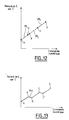
- Figure 12 shows a curve representing the delay between input E and output S of the circuit of the Figure 11 as a function of the digital control signal.
- Five characteristic points are visible on the curve.
- Point a corresponds to the minimum delay, therefore in case these are the signals e0 and r1 which enter into the combination circuit, with 100% of the current which goes into module U0.
- Point b corresponds to maximum delay when e0 and r1 enter the circuit combination with 100% of the current flowing in the module U1.
- the segment between a and b constitutes the range Pl1.
- This second range Pl2 ends with a point c which corresponds to the maximum delay between r1 and r2 with 100% of the current flowing through the U0 module.
- the advantage of recommended connection mode in fact does not switch than a multiplexer (MUX0) taking into account the symmetrical character of the circuit of FIGS. 11 and 15. Then it is the turn of the MUX1 multiplexer to switch, the signal r1 giving way to signal r3.
- MUX0 multiplexer
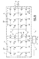
- Figures 14 and 15 show according to the invention a solution to this problem.
- FIG. 14 shows the circuit of Figure 10.
- These non-variable resistances no longer depend on K. They ensure that each module U0 and U1 contributes permanently to the charging or discharging of the line L.
- the advantage of such an assembly will be specified with the study of FIG. 15 which offers a more detailed description of this circuit.
- FIG. 15 shows the circuit of FIG. 11.
- the multiplexers MUX0 and MUX1 and the buffer memories T1, T2 and T3 constitute the delay circuit D1.
- a branch has been added in parallel. These branches each have in series two P-channel transistors in series and two N-channel transistors in series.
- the P channel transistors P01 and P02 for U0, P11 and P12 for U1 operate in the same way as the P channel transistors already present in the circuit shown in Figure 11 in the load circuits of U0 and U1.
- the new N channel transistors, N01 and N02 for U0, N11 and N12 for U1, intervene similarly in the discharge circuits of U0 and U1.
- the added transistors P01, N01, P11 and N11 which act as switches are always connected to the signals m0 and m1. But those which serve as variable resistors, namely P02, N02, P12 and N12, are permanently supplied: the transistors added to channel N, N02 and N12, are connected to the potential Vdd and the transistors added to channel P, P02 and P12 are related to the Vss potential. They do not depend on a K or K * command. Also, additional branches will always drive. This compensates for the leaks and the load distribution problems observed when switching the multiplexers, which result in a horizontal or slightly decreasing flat area.
- the current distributions in the modules U0 and U1 are slightly modified: we can no longer have 100% of the current flowing in one module and 0% in the other.
- each module typically comprises three transistors controlled by the commands K and K * .
- the added transistor which is permanently connected to the potential Vdd or Vss will typically be smaller than the other three transistors, so that there is a maximum of 90% of the current which can pass through a module U0 or U1. This means that the permanently supplied transistor must be three times smaller than the other transistors.
- transistors controlled by the coefficients K0, K1, etc ... have increasing grid widths binary (1, 2, 4, etc ).
- the transistor added in the additional branch has half grid width from the smallest of the previous grid widths.
- the branch added has a grid width half from that of other branches.
- FIGS 16a, 16b, 16c, 16d and 16e allow to explain what is happening now on the first beach. In their description, it will often be done reference to the circuit of figure 15.
- Figures 16a and 16b are the timing diagrams of the signals m0 and m1 offset by a time T.
- the origin of the time is defined when m0 switches to 0.
- the curves Co and Ci respectively correspond to the charge of the capacitor C1 before and after the introduction of the permanently connected transistors.
- the times t1 and ti are respectively the times taken, before and after the improvement of the invention, by the signal Sk to reach the threshold value S2. There is therefore at the start of the range a delay ti greater than t1. It can be seen in FIG. 16c that once m1 has switched to 0, the charge of the capacitor C1 is faster than before. This is explained by the fact that P11 then participates in the charge of C1.
- the new delay at the start of the track is greater than that in the absence of permanently connected branches, and there is less important at the end of the range.
- the points S1 and B1 are those of the new delay curve.
- the point S1 and B1 are respectively above and below points A and B above ( Figure 12).
- Figure 17 explains the change of range. She shows in dashes the real curve of the delays caused without improvement, a b b 'c c' d 'which is a broken line. The delay curve obtained with the improvement of the invention is shown in lines full. The latter goes through the points a1 b1 b'1 c1 it's 1 of 1 that are all aligned. The delay associated with point b1 is much lower than that associated with point b while the delay associated with point b'1 is greater to that associated with point b '.
- the digital control can therefore order more effectively the values of the coefficients ki and the tilting of the multiplexers. Indeed, if this command results from a slave action, the fact that the servo has a negative slope (b b ', c c ') and in particular a vertex, in b or in c, of the gain curve, causes this servo to oscillate around the value associated with point b.
- Figure 17 also shows the comparison between the delay curves obtained: the curve Co1 representative of the delay time in the absence of branches permanently connected, and the Co2 curve characteristic of the delay time for the circuit including branches permanently connected.
- the Co2 curve that we are approaching a optimal linearity; the delay is so anyway always increased.
Abstract
Description
- un circuit primaire, recevant le signal d'entrée et fournissant des premier et second signaux intermédiaires présentant entre eux un retard fixe,
- un circuit de combinaison à deux entrées, fournissant en sortie un signal de combinaison résultant d'une superposition avec une pondération fonction de la grandeur de commande et un effet d'intégration des signaux appliqués sur ses entrées, les signaux intermédiaires étant appliqués aux deux entrées du circuit de combinaison,
- un circuit de mise en forme recevant le signal de combinaison, fournissant le signal de sortie, et présentant un effet de seuil,
- une entrée de commande recevant une grandeur de commande représentative de la consigne,
- une ligne commune avec un condensateur relié à cette ligne commune et à un potentiel d'alimentation,
- un premier et un second module de charge et décharge de la ligne commune commandés respectivement par les premier et second signaux intermédiaires, le potentiel de la ligne commune constituant la mesure du signal de combinaison,
- la figure 1 représente le schéma de principe d'un circuit à retard variable à plusieurs plages de retard;
- les figures 2a à 2c, 4a à 4c, 6a à 6c et 8a à 8c présentent des chronogrammes permettant d'expliquer le fonctionnement du circuit de la figure 1;
- les figures 3, 5, 7, 9 montrent les variations du retard en fonction de la grandeur de commande pour différents dimensionnements du circuit de la figure 1;
- la figure 10 représente le schéma de principe d'une réalisation CMOS d'un circuit à retard variable à plusieurs plages de retard;
- la figure 11 représente une réalisation détaillée en technologie CMOS du circuit à retard variable à plusieurs plages de retard;
- la figure 12 présente une courbe théorique représentant des temps de retard en fonction de la commande numérique;
- la figure 13 montre une courbe représentant les temps de retard effectivement observés dans le circuit à retard variable à plusieurs plages de retard en fonction de la commande numérique;
- la figure 14 représente l'amélioration amenée par l'invention du circuit présenté à la figure 10 conduisant à une amélioration de la linéarité du retard en fonction de la commande numérique;
- la figure 15 représente l'amélioration amenée par l'invention du circuit présenté à la figure 11 conduisant à une amélioration de la linéarité du retard en fonction de la commande numérique;
- la figure 16 présente une comparaison, sur une plage, des temps de retard obtenus en fonction de la commande numérique, avec les circuits des figures 11 et 15;
- la figure 17 présente une comparaison entre des temps de retard obtenus avec le circuit de la figure 11 et ceux obtenus avec le circuit de la figure 15.
Claims (7)
- Circuit à retard pour fournir un signal de sortie (sK) présentant un retard (Θ) par rapport à un signal d'entrée (e0), le retard (Θ) étant réglable en fonction d'une consigne de retard (CN), le circuit à retard comportantle circuit de combinaison comportantun circuit primaire (D1), recevant le signal d'entrée (e0) et fournissant des premier et second signaux intermédiaires (m0, m1) présentant entre eux un retard fixe (T) ,un circuit de combinaison (C) à deux entrées (X, Y), les signaux intermédiaires (m0, m1) étant appliqués aux entrées (X, Y), fournissant en sortie un signal de combinaison (fK) résultant d'une superposition avec une pondération fonction de la grandeur de commande (K) et un effet d'intégration des signaux appliqués sur ses entrées (X, Y),un circuit de mise en forme recevant le signal de combinaison, fournissant le signal de sortie SK, et présentant un effet de seuil,le circuit à retard étant caractérisé en ce que chaque module (U0, U1) comporte un circuit de décharge (DC) et un circuit de charge (PC) comportant chacun des moyens interrupteurs (P0, N0, P1, N1) contrôlant la connexion entre la ligne commune (L) et respectivement un premier et un second potentiel d'alimentation (Vss, Vdd) d'une part par l'intermédiaire d'une résistance variable (R0, RO*, R1, R1*), d'autre part par une résistance non variable (R0f, R0f*, R1f, R1f*) assurant la participation permanente des deux modules (U0 et U1) à la charge ou la décharge du condensateur (C1) et en ce que les moyens interrupteurs (P0, N0, P1, N1) du circuit de décharge (DC) et du circuit de charge (PC) de chaque module (U0, U1) sont activés par les signaux intermédiaires (m0, m1).une entrée de commande (CD) recevant une grandeur de commande (K) représentative de la consigne (CN),une ligne commune (L) avec un condensateur (C1) relié à cette ligne commune et à un potentiel d'alimentation,un premier et un second module de charge et décharge (U0, U1) de la ligne commune (L) commandés respectivement par les premier et second signaux intermédiaires (m0, m1), le potentiel de la ligne commune (L) constituant la mesure du signal de combinaison (fK),
- Circuit à retard selon la revendication 1, caractérisé en ce que le retard fixe (T) est inférieur à un temps de transition (tm) que présente le signal de combinaison (fK) lorsque le circuit de combinaison (C) reçoit seulement un des deux signaux (m0, m1).
- Circuit selon l'une des revendications 1 ou 2, caractérisé en ce que la pondération consiste à pondérer par un coefficient de pondération chacun des signaux en entrée du circuit de combinaison (C), les valeurs des coefficients de pondération étant fonction de la grandeur de commande (K), la somme des deux coefficients de pondération étant constante, la résistance variable (R0, R0*, R1, R1* ) des circuits de décharge et de charge (DC, PC) de chaque module (U0, U1) étant commandée de façon à prendre une valeur inversement proportionnelle au coefficient de pondération d'un des signaux intermédiaires (m0, m1).
- Circuit à retard selon une des revendications 1 à 3, caractérisé en ce que les résistances variables (R0, RO*, R1, R1*) de chaque module (U0, U1) sont réalisées au moyen d'un ensemble de résistances élémentaires pouvant être branchées sélectivement en parallèle en fonction du coefficient de pondération du signal intermédiaire associé (m0, m1) audit module (U0, U1).
- Circuit à retard selon l'une des revendications 1 à 4, caractérisé en ce que les résistances variables (R0, R0*, R1, R1*), les résistances non variables (R0f, R0f*, R1f, R1f*) et les interrupteurs (P0, N0, P1, N1) sont formés par les chemins drain-source de transistors MOS dont les grilles sont commandées en fonction des coefficients de pondération, par les signaux associés (m0, m1) ou par des potentiels constants.
- Circuit à retard selon l'une des revendications 1 à 5, caractérisé en ce qu'un module de charge et de décharge comporte trois branches commandées par un signal de pondération (K) et une branche en conduction permanente.
- Circuit à retard selon l'une des revendications 1 à 6, caractérisé en ce que le circuit à retard le circuit primaire (D1) est réalisé au moyen d'un jeu de mémoires tampons (T1, T2, T3) en série, retardant pour chacune le signal à sa sortie d'un retard (T), à la sortie desquelles on obtient au moins des premier et deuxième signaux retardés (r1, r2), le signal d'entrée (e0) et les signaux retardés (r1, r2) étant appliqués aux entrées d'un premier et d'un deuxième multiplexeur (MUX0, MUX1) qui fournissent les premier et deuxième signaux intermédiaires (m0, m1).
Applications Claiming Priority (2)
| Application Number | Priority Date | Filing Date | Title |
|---|---|---|---|
| FR9711022A FR2767982B1 (fr) | 1997-09-04 | 1997-09-04 | Circuit a retard variable |
| FR9711022 | 1997-09-04 |
Publications (2)
| Publication Number | Publication Date |
|---|---|
| EP0901227A1 true EP0901227A1 (fr) | 1999-03-10 |
| EP0901227B1 EP0901227B1 (fr) | 2004-01-21 |
Family
ID=9510769
Family Applications (1)
| Application Number | Title | Priority Date | Filing Date |
|---|---|---|---|
| EP98402152A Expired - Lifetime EP0901227B1 (fr) | 1997-09-04 | 1998-08-31 | Circuit à retard variable |
Country Status (5)
| Country | Link |
|---|---|
| US (1) | US6169436B1 (fr) |
| EP (1) | EP0901227B1 (fr) |
| JP (1) | JP3470946B2 (fr) |
| DE (1) | DE69821175D1 (fr) |
| FR (1) | FR2767982B1 (fr) |
Cited By (2)
| Publication number | Priority date | Publication date | Assignee | Title |
|---|---|---|---|---|
| EP1398900A1 (fr) * | 2002-09-13 | 2004-03-17 | St Microelectronics S.A. | Transformation d'un signal périodique en un signal de fréquence ajustable |
| EP2354825A1 (fr) | 2010-02-03 | 2011-08-10 | Tyco Electronics Nederland B.V. | Ensemble de fermeture pour connecteur, élément de réduction de tension et procédé |
Families Citing this family (15)
| Publication number | Priority date | Publication date | Assignee | Title |
|---|---|---|---|---|
| EP0932110B1 (fr) * | 1998-01-22 | 2003-02-19 | Bull S.A. | Procédé d'évaluation de performances de circuits à très haute intégration |
| US6970313B1 (en) | 1999-03-31 | 2005-11-29 | Matsushita Electric Industrial Co., Ltd. | Write compensation circuit and signal interpolation circuit of recording device |
| JP3297738B2 (ja) * | 2000-02-16 | 2002-07-02 | 東北大学長 | Cmos多数決回路 |
| US6684311B2 (en) * | 2001-06-22 | 2004-01-27 | Intel Corporation | Method and mechanism for common scheduling in a RDRAM system |
| JP3810316B2 (ja) * | 2001-12-26 | 2006-08-16 | 沖電気工業株式会社 | 周波数逓倍回路 |
| US7515656B2 (en) * | 2002-04-15 | 2009-04-07 | Fujitsu Limited | Clock recovery circuit and data receiving circuit |
| DE602004009137T2 (de) * | 2003-07-31 | 2008-06-19 | Stmicroelectronics Pvt. Ltd. | Digitaler Taktmodulator |
| US7116147B2 (en) * | 2004-10-18 | 2006-10-03 | Freescale Semiconductor, Inc. | Circuit and method for interpolative delay |
| US7323918B1 (en) * | 2006-08-08 | 2008-01-29 | Micrel, Incorporated | Mutual-interpolating delay-locked loop for high-frequency multiphase clock generation |
| US7737750B2 (en) * | 2007-01-16 | 2010-06-15 | Infineon Technologies Ag | Method and device for determining trim solution |
| TWI364165B (en) * | 2008-07-21 | 2012-05-11 | Univ Nat Chiao Tung | Absolute delay generating device |
| WO2012082140A1 (fr) | 2010-12-17 | 2012-06-21 | Agilent Technologies, Inc. | Appareil et procédé pour ajustement temporel de signal d'entrée |
| US9306551B2 (en) * | 2013-01-22 | 2016-04-05 | Mediatek Inc. | Interpolator and interpolation cells with non-uniform driving capabilities therein |
| US9106230B1 (en) * | 2013-03-14 | 2015-08-11 | Altera Corporation | Input-output circuitry for integrated circuits |
| JP6297575B2 (ja) * | 2013-08-19 | 2018-03-20 | 国立研究開発法人科学技術振興機構 | 再構成可能な遅延回路、並びにその遅延回路を用いた遅延モニタ回路、ばらつき補正回路、ばらつき測定方法及びばらつき補正方法 |
Citations (4)
| Publication number | Priority date | Publication date | Assignee | Title |
|---|---|---|---|---|
| EP0317758A2 (fr) * | 1987-11-25 | 1989-05-31 | Tektronix, Inc. | Méthode pour produire un signal retardé et circuit de retard réglable |
| EP0562904A1 (fr) * | 1992-03-24 | 1993-09-29 | Bull S.A. | Procédé et dispositif de réglage de retard à plusieurs gammes |
| US5327031A (en) * | 1992-03-24 | 1994-07-05 | Bull S.A. | Variable-delay circuit |
| EP0606979A2 (fr) * | 1993-01-15 | 1994-07-20 | National Semiconductor Corporation | Ligne à retard numérique CMOS à prises multiples non inversantes |
-
1997
- 1997-09-04 FR FR9711022A patent/FR2767982B1/fr not_active Expired - Fee Related
-
1998
- 1998-08-31 EP EP98402152A patent/EP0901227B1/fr not_active Expired - Lifetime
- 1998-08-31 DE DE69821175T patent/DE69821175D1/de not_active Expired - Lifetime
- 1998-09-03 US US09/146,602 patent/US6169436B1/en not_active Expired - Fee Related
- 1998-09-04 JP JP25120698A patent/JP3470946B2/ja not_active Expired - Fee Related
Patent Citations (4)
| Publication number | Priority date | Publication date | Assignee | Title |
|---|---|---|---|---|
| EP0317758A2 (fr) * | 1987-11-25 | 1989-05-31 | Tektronix, Inc. | Méthode pour produire un signal retardé et circuit de retard réglable |
| EP0562904A1 (fr) * | 1992-03-24 | 1993-09-29 | Bull S.A. | Procédé et dispositif de réglage de retard à plusieurs gammes |
| US5327031A (en) * | 1992-03-24 | 1994-07-05 | Bull S.A. | Variable-delay circuit |
| EP0606979A2 (fr) * | 1993-01-15 | 1994-07-20 | National Semiconductor Corporation | Ligne à retard numérique CMOS à prises multiples non inversantes |
Cited By (4)
| Publication number | Priority date | Publication date | Assignee | Title |
|---|---|---|---|---|
| EP1398900A1 (fr) * | 2002-09-13 | 2004-03-17 | St Microelectronics S.A. | Transformation d'un signal périodique en un signal de fréquence ajustable |
| FR2844655A1 (fr) * | 2002-09-13 | 2004-03-19 | St Microelectronics Sa | Transformation d'un signal periodique en un signal de frequence ajustable |
| US6975173B2 (en) | 2002-09-13 | 2005-12-13 | Stmicroelectronics S.A. | Transformation of a periodic signal into an adjustable-frequency signal |
| EP2354825A1 (fr) | 2010-02-03 | 2011-08-10 | Tyco Electronics Nederland B.V. | Ensemble de fermeture pour connecteur, élément de réduction de tension et procédé |
Also Published As
| Publication number | Publication date |
|---|---|
| FR2767982B1 (fr) | 2001-11-23 |
| FR2767982A1 (fr) | 1999-03-05 |
| JP3470946B2 (ja) | 2003-11-25 |
| US6169436B1 (en) | 2001-01-02 |
| EP0901227B1 (fr) | 2004-01-21 |
| DE69821175D1 (de) | 2004-02-26 |
| JPH11168364A (ja) | 1999-06-22 |
Similar Documents
| Publication | Publication Date | Title |
|---|---|---|
| EP0901227B1 (fr) | Circuit à retard variable | |
| EP0562904B1 (fr) | Procédé et dispositif de réglage de retard à plusieurs gammes | |
| EP0562905B1 (fr) | Circuit à retard variable | |
| FR2635239A1 (fr) | Element a retard pour circuit numerique | |
| EP0474534A1 (fr) | Circuit à constante de temps réglable et application à un circuit à retard réglable | |
| FR2752114A1 (fr) | Oscillateur et boucle a verrouillage de phase utilisant un tel oscillateur | |
| EP2769473B1 (fr) | Convertisseur numerique-analogique | |
| FR2800938A1 (fr) | Circuit d'excitation de commutation, circuit de commutation utilisant un tel circuit d'excitation, et circuit convertisseur numerique-analogique utilisant ce circuit de commutation | |
| FR2774234A1 (fr) | Dispositif a semiconducteur | |
| EP3667915A1 (fr) | Circuit retardateur | |
| EP2327160B1 (fr) | Compteur analogique et imageur incorporant un tel compteur | |
| EP3654534A1 (fr) | Cellule logique capacitive | |
| CA2057824C (fr) | Dispositif de retard reglable | |
| WO2005055431A1 (fr) | Convertisseur analogique-numerique rapide | |
| FR2911449A1 (fr) | Filtre echantillonne a reponse impulsionnelle finie | |
| FR2623932A1 (fr) | Memoire comportant un circuit de charge de ligne de bit a impedance variable | |
| FR2461958A1 (fr) | Circuit de comparaison de phase | |
| FR2572574A1 (fr) | Cellule de memoire de registre a decalage | |
| EP0835550B1 (fr) | Comparateur de phase sans zone morte | |
| EP0872960A1 (fr) | Dispositif d'alignement numérique. | |
| EP3667914B1 (fr) | Calibration d'un circuit retardateur | |
| EP1845619A1 (fr) | Circuit tampon comprenant des moyens de contrôle de la pente du signal de sortie | |
| FR2767243A1 (fr) | Dispositif adaptateur symetrique de commutation d'un signal logique | |
| EP0332499B1 (fr) | Comparateur rapide avec étage de sortie fonctionnant en deux phases | |
| FR2497033A1 (fr) | Attenuateur pour signal electrique |
Legal Events
| Date | Code | Title | Description |
|---|---|---|---|
| PUAI | Public reference made under article 153(3) epc to a published international application that has entered the european phase |
Free format text: ORIGINAL CODE: 0009012 |
|
| AK | Designated contracting states |
Kind code of ref document: A1 Designated state(s): DE FR GB IT |
|
| AX | Request for extension of the european patent |
Free format text: AL;LT;LV;MK;RO;SI |
|
| 17P | Request for examination filed |
Effective date: 19990331 |
|
| AKX | Designation fees paid |
Free format text: DE FR GB IT |
|
| RAP1 | Party data changed (applicant data changed or rights of an application transferred) |
Owner name: STMICROELECTRONICS S.A. |
|
| GRAP | Despatch of communication of intention to grant a patent |
Free format text: ORIGINAL CODE: EPIDOSNIGR1 |
|
| GRAS | Grant fee paid |
Free format text: ORIGINAL CODE: EPIDOSNIGR3 |
|
| GRAA | (expected) grant |
Free format text: ORIGINAL CODE: 0009210 |
|
| AK | Designated contracting states |
Kind code of ref document: B1 Designated state(s): DE FR GB IT |
|
| PG25 | Lapsed in a contracting state [announced via postgrant information from national office to epo] |
Ref country code: IT Free format text: LAPSE BECAUSE OF FAILURE TO SUBMIT A TRANSLATION OF THE DESCRIPTION OR TO PAY THE FEE WITHIN THE PRE;WARNING: LAPSES OF ITALIAN PATENTS WITH EFFECTIVE DATE BEFORE 2007 MAY HAVE OCCURRED AT ANY TIME BEFORE 2007. THE CORRECT EFFECTIVE DATE MAY BE DIFFERENT FROM THE ONE RECORDED.SCRIBED TIME-LIMIT Effective date: 20040121 |
|
| REG | Reference to a national code |
Ref country code: GB Ref legal event code: FG4D Free format text: NOT ENGLISH |
|
| REF | Corresponds to: |
Ref document number: 69821175 Country of ref document: DE Date of ref document: 20040226 Kind code of ref document: P |
|
| GBT | Gb: translation of ep patent filed (gb section 77(6)(a)/1977) |
Effective date: 20040226 |
|
| PG25 | Lapsed in a contracting state [announced via postgrant information from national office to epo] |
Ref country code: DE Free format text: LAPSE BECAUSE OF FAILURE TO SUBMIT A TRANSLATION OF THE DESCRIPTION OR TO PAY THE FEE WITHIN THE PRESCRIBED TIME-LIMIT Effective date: 20040422 |
|
| PLBE | No opposition filed within time limit |
Free format text: ORIGINAL CODE: 0009261 |
|
| STAA | Information on the status of an ep patent application or granted ep patent |
Free format text: STATUS: NO OPPOSITION FILED WITHIN TIME LIMIT |
|
| 26N | No opposition filed |
Effective date: 20041022 |
|
| PGFP | Annual fee paid to national office [announced via postgrant information from national office to epo] |
Ref country code: FR Payment date: 20060808 Year of fee payment: 9 |
|
| PGFP | Annual fee paid to national office [announced via postgrant information from national office to epo] |
Ref country code: GB Payment date: 20060830 Year of fee payment: 9 |
|
| GBPC | Gb: european patent ceased through non-payment of renewal fee |
Effective date: 20070831 |
|
| REG | Reference to a national code |
Ref country code: FR Ref legal event code: ST Effective date: 20080430 |
|
| PG25 | Lapsed in a contracting state [announced via postgrant information from national office to epo] |
Ref country code: FR Free format text: LAPSE BECAUSE OF NON-PAYMENT OF DUE FEES Effective date: 20070831 |
|
| PG25 | Lapsed in a contracting state [announced via postgrant information from national office to epo] |
Ref country code: GB Free format text: LAPSE BECAUSE OF NON-PAYMENT OF DUE FEES Effective date: 20070831 |