EP0897146A2 - Appareil de traitement arithmétique et procédé du même - Google Patents
Appareil de traitement arithmétique et procédé du même Download PDFInfo
- Publication number
- EP0897146A2 EP0897146A2 EP98402033A EP98402033A EP0897146A2 EP 0897146 A2 EP0897146 A2 EP 0897146A2 EP 98402033 A EP98402033 A EP 98402033A EP 98402033 A EP98402033 A EP 98402033A EP 0897146 A2 EP0897146 A2 EP 0897146A2
- Authority
- EP
- European Patent Office
- Prior art keywords
- data
- register
- processing
- internal memory
- stored
- Prior art date
- Legal status (The legal status is an assumption and is not a legal conclusion. Google has not performed a legal analysis and makes no representation as to the accuracy of the status listed.)
- Withdrawn
Links
- 238000012545 processing Methods 0.000 title claims abstract description 202
- 238000003672 processing method Methods 0.000 title claims description 7
- 230000015654 memory Effects 0.000 claims abstract description 292
- 230000006870 function Effects 0.000 claims description 14
- 238000012546 transfer Methods 0.000 claims description 13
- 238000000034 method Methods 0.000 description 8
- 239000000872 buffer Substances 0.000 description 3
- 238000004891 communication Methods 0.000 description 3
- 238000013461 design Methods 0.000 description 3
- 230000004044 response Effects 0.000 description 2
- 230000001934 delay Effects 0.000 description 1
- 230000003111 delayed effect Effects 0.000 description 1
- 238000010586 diagram Methods 0.000 description 1
- 239000000203 mixture Substances 0.000 description 1
- 238000012986 modification Methods 0.000 description 1
- 230000004048 modification Effects 0.000 description 1
- 230000003068 static effect Effects 0.000 description 1
Images


Classifications
-
- G—PHYSICS
- G06—COMPUTING; CALCULATING OR COUNTING
- G06F—ELECTRIC DIGITAL DATA PROCESSING
- G06F9/00—Arrangements for program control, e.g. control units
- G06F9/06—Arrangements for program control, e.g. control units using stored programs, i.e. using an internal store of processing equipment to receive or retain programs
- G06F9/30—Arrangements for executing machine instructions, e.g. instruction decode
- G06F9/30098—Register arrangements
- G06F9/30141—Implementation provisions of register files, e.g. ports
-
- G—PHYSICS
- G06—COMPUTING; CALCULATING OR COUNTING
- G06F—ELECTRIC DIGITAL DATA PROCESSING
- G06F9/00—Arrangements for program control, e.g. control units
- G06F9/06—Arrangements for program control, e.g. control units using stored programs, i.e. using an internal store of processing equipment to receive or retain programs
- G06F9/30—Arrangements for executing machine instructions, e.g. instruction decode
- G06F9/30098—Register arrangements
- G06F9/30101—Special purpose registers
-
- G—PHYSICS
- G06—COMPUTING; CALCULATING OR COUNTING
- G06F—ELECTRIC DIGITAL DATA PROCESSING
- G06F9/00—Arrangements for program control, e.g. control units
- G06F9/06—Arrangements for program control, e.g. control units using stored programs, i.e. using an internal store of processing equipment to receive or retain programs
- G06F9/30—Arrangements for executing machine instructions, e.g. instruction decode
- G06F9/34—Addressing or accessing the instruction operand or the result ; Formation of operand address; Addressing modes
- G06F9/35—Indirect addressing
-
- G—PHYSICS
- G06—COMPUTING; CALCULATING OR COUNTING
- G06F—ELECTRIC DIGITAL DATA PROCESSING
- G06F9/00—Arrangements for program control, e.g. control units
- G06F9/06—Arrangements for program control, e.g. control units using stored programs, i.e. using an internal store of processing equipment to receive or retain programs
- G06F9/30—Arrangements for executing machine instructions, e.g. instruction decode
- G06F9/38—Concurrent instruction execution, e.g. pipeline, look ahead
- G06F9/3824—Operand accessing
Definitions
- the present invention relates to a microprocessor and a processing method thereof.
- microprocessors When classifying microprocessors by general design concepts, they can be divided into, for example, a reduced instruction set computer (RISC) type and a complex instruction set computer (CISC) type.
- RISC reduced instruction set computer
- CISC complex instruction set computer
- Program execution time number of executed instructions (IC) x average number of clock cycles required per instruction (CPI) x clock cycle time (CCT)
- a RISC type microprocessor is based on the design concept of making the CPI in the above formula (1) as close as possible to 1 by using instruction pipeline processing.
- instructions are made a fixed single length and a register-register format (load/store type architecture: in which the only possible source operand for a processing instruction is a register operand) is used as an instruction format from the viewpoint of simplifying the functions of instructions functions so as to be suitable for instruction pipeline processing.
- a register-register format load/store type architecture: in which the only possible source operand for a processing instruction is a register operand
- a RISC type microprocessor performs static code scheduling by a compiler so as to prevent delays in the instruction pipeline processing.
- a CISC type microprocessor is based on the design concept of improving the level of functions of instructions so as to eliminate the IC of the above formula (1).
- instructions are made a plurality of fixed lengths or variable lengths, and the instruction format includes a mixture of the register-memory format and memory-memory format (where a memory operand is also possible for a source operand of a processing instruction). Namely, direct processing between a register and memory is made possible.
- a RISC type microprocessor When data in a memory is processed by an arithmetic and logic unit (ALU), a RISC type microprocessor requires at least two instructions, a load instruction and a store instruction, for accessing the memory.
- ALU arithmetic and logic unit
- a CISC type microprocessor does not require any instruction specifically for accessing the memory.
- a large bit field is required in an instruction for designating a memory address.
- a variable length instruction is used in many cases.
- the decoding circuit tends to become complicated and large in size when using variable length instructions. Therefore, in a CISC type microprocessor, at the present time, program execution time is being shortened by using super scalar techniques or out-of-order techniques to speed up the processing of data in the memory.
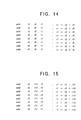
- Figure 20 is a view for explaining general-purpose registers in conventional RISC type and the CISC type microprocessors.
- a conventional microprocessor is provided with, for example, 16 general-purpose registers. Assume that these 16 general-purpose registers are referred to as r0 to r15.
- registers When these registers are mounted in a processor architecture comprised of a set of 3-operand processing instructions, three ports in total, that is, two read ports and one write port, are necessary
- the instruction shown in Fig. 21 is an instruction to execute "r2 ⁇ r3+r4".
- the registers r0 to r15 are general-purpose ones and are used for temporarily holding values.
- a load/store instruction is executed for a general-purpose register in order to realize a load/store operation on a memory.
- CISC processors it is possible to designate data in a memory as an operand of an ALU processing instruction. In this case, however, a general-purpose register is not used. A memory buffer is used directly.
- a five-stage or eight-stage pipeline structure is often used.
- the "R3000" (product name) of the MIPS Co. uses a five-stage pipeline comprising an instruction fetch (IF) stage, an instruction decode (DEC) stage, an arithmetic logic unit processing (ALU) stage, a memory (MEM) stage, and a write back (WB) stage.
- IF instruction fetch
- DEC instruction decode
- ALU arithmetic logic unit processing
- MEM memory
- WB write back
- This processor fetches (reads) an instruction in the first (IF) stage and decodes the instruction in the second (DEC) stage. Note that if the instruction designates a general-purpose register as a source register, the processor decodes the instruction in the DEC stage, then reads the data from the general-purpose register.
- the third (ALU) stage executes an ALU processing instruction. Note that when the fetched instruction is not an ALU instruction, nothing is done in the ALU stage and the data is output to the ALU output port as it is.
- the processor when the fetched instruction is a memory access instruction, the processor outputs a memory address used for memory access to a memory unit for accessing the memory.
- the processor writes back the result of the ALU processing in the general-purpose register. If the instruction is a memory read instruction (load instruction), it receives a value from the memory unit and writes it in the general-purpose register.
- load instruction a memory read instruction
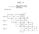
- a processor using a five-stage pipeline performs, by multiplexing, in a clock cycle X, for example, the WB stage of a code C1, the MEM stage of a code C2, the ALU stage of a code C3, the DEC stage of a code C4, and the IF stage of a code C5.
- Fig. 23 in order to multiplex the desired instruction with these instructions, for example, use of the five-stage pipeline structure shown in Fig. 23 is convenient. Namely, the memory access instruction and other instructions can be executed simultaneously. Since it is assumed that there is only one system (1 set) of paths for memory access, it is impossible to execute memory read and memory write operations at the same MEM stage simultaneously.
- unused pipeline stages end up occurring.
- the function of the MEM stage is not used.
- the function of the ALU stage is not used. Note that the address generating processing for memory access is performed in units other than the ALU.
- the processor loads the data at the memory address indicated by the register r10 to the register r2 by the instruction "1w r2, 0 (r10)”.
- the processor adds the values in the registers r2 and r9 and inserts the result in the register r3 by the instruction "addu r3, r2, r9”.
- it stores (writes back) the value in the register r3 in the memory address indicated by the register r11 by the instruction "sw r3, 0 (r11)”.
- These operations are written by three instructions. Since each instruction requires at least one clock cycle for execution, three cycles are required to execute the three instructions. In actuality, one more cycle is required because the data read (loaded) from the memory cannot be referred to by the immediately succeeding instruction.
- the starting address of the source data of the addition processing on the memory is set using the register r10, while the starting address of the destination data is set using the register r11.
- An object of the present invention is to provide a microprocessor which is improved in its processing capability, and a processing method for the same, which can effectively perform processing associated with a predetermined pattern of consecutive accesses to a memory address space.
- a microprocessor comprising: an internal memory for storing data to be processed; a data pointer register for storing an address of said internal memory and automatically updating a stored address in accordance with a predetermined pattern when there is a predetermined pattern in access to said internal memory; a decoding means for decoding instructions; a plurality of general-purpose registers including a data register for storing data read from an address, of said internal memory, stored in said data pointer register, in accordance with a request for reading out data stored in said internal memory and for writing stored data at an address, of said internal memory, stored in said data pointer register, in accordance with a request for writing data to said internal memory; and a processing means for performing processing by using data stored in said general-purpose registers and for writing the result of processing in said general-purpose registers in accordance with the result of decoding of said decoding means.
- the data register reads the data from an updated address of said memory immediately after an address stored in said data pointer register is updated.
- the data register terminates the function of reading the data from an updated address of said memory immediately after an address stored in said data pointer register is updated when continuously and repeatedly writing data in said internal memory.
- the plurality of general-purpose registers include a plurality of data registers and there are a plurality of data pointer registers corresponding to these plurality of data registers.
- the memory address space of said internal memory is divided into a plurality of banks and each of the plurality of data pointer registers stores only addresses in a corresponding bank among said plurality of banks.
- the microprocessor of the first aspect of the present invention further comprises a switching means for switching interconnections among said data register, said plurality of general-purpose registers other than said data register, and said processing means.
- a mode of connection between said data register and said processing means and a mode of connection between said plurality of general-purpose registers other than said data register and said processing means are equivalent.
- the microprocessor of a second aspect of the present invention comprises: an instruction memory for storing a plurality of instructions; a program counter for designating an address of said instruction memory where an instruction to be next executed is stored; a decoding means for decoding instructions; an internal memory for storing data to be processed; a first data pointer register and a second data pointer register for storing addresses of said internal memory; a plurality of general-purpose registers including a first data register for storing data read from an address, of said internal memory, stored in said first data pointer register, in accordance with a request for reading out data stored in said internal memory, and a second data register for writing stored data at an address, of said internal memory, stored in said second data pointer register, in accordance with a request for writing data to said internal memory; and a processing means for performing processing by using data stored in said general-purpose registers and for writing the result of processing in said general-purpose registers in accordance with the result of decoding of said decoding means, and performing four-stage pipeline processing comprising,
- the memory address space of said internal memory is divided into a plurality of banks, said first data pointer register and said second data pointer register access different banks of said internal memory, said decoding processing transfers data from said first data register to said processing means, and said write back processing transfers the results of said processing to said second data register.
- the first data pointer register and said second data pointer register automatically update an address stored in said first data pointer register and said second data pointer register in accordance with a predetermined pattern when there is a predetermined pattern in access to said internal memory.
- processing for reading data from an address of said internal memory stored in said first data pointer register and storing it in said first data register and processing for writing the data written in said second data register at an address of said internal memory stored in said second data pointer register are performed in parallel with said four-stage pipeline processing.
- a microprocessor comprising: an internal memory for storing data to be processed; a data pointer register for storing an address of said internal memory; a decoding means for decoding instructions; a data register for storing data read from an address, of said internal memory, stored in said data pointer register, in accordance with a request for reading out data stored in said internal memory, and for writing stored data at an address, of said internal memory, stored in said data pointer register, in accordance with a request for writing data to said internal memory; a plurality of general-purpose registers; and a processing means for performing processing by using data stored in at least one of said data register and said general-purpose registers and writing the result of processing in said data register or said general-purpose registers based on the result of decoding of said decoding means.
- the processing method of the present invention comprises performing four-stage pipeline processing comprising, multiplexed, instruction fetching processing for reading an instruction from an address, of an instruction memory, designated by a program counter; decoding processing for decoding said fetched instruction; processing performed using data stored in a first data register based on the result of said decoding processing; and write back processing for writing the result of processing of said processing in a second data register and performing: processing for reading data from an address, of an internal memory, stored in a first data pointer register, and storing it in said first data register and processing for writing back the data written in said second data register at an address, of said internal memory, stored in a second data pointer register, in parallel with said four-stage pipeline processing.
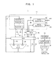
- Figure 1 is a view of the configuration of the microprocessor 1 of a first embodiment.
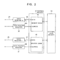
- the microprocessor 1 comprises a general-purpose register module 11, multiplexers 12 and 16, an arithmetic and logic unit (ALU) 13, an instruction page memory 35, a decoder 36, shown in Fig. 1, and DP registers 30 and 31 and an internal memory 47, shown in Fig. 2, and is configured with these included in one chip.
- ALU arithmetic and logic unit
- the general-purpose register module 11 is a set of registers comprising, for example, the 32-bit registers r0 to r15 used for general purposes.
- the number of registers constituting the general-purpose register module 11 depends largely on the set of instructions or the chip architecture. Generally, it is set in the range of 8 to 32.
- the general-purpose register module 11 is provided with seven ports W, RA, RB, MA, MB, DA, and DB as shown in Fig. 1.
- the port W is a write port.
- the data output from the port AOUT of the ALU 13 is written in the general-purpose register module 11 via a bus 23 and the port W.
- the ports MA and MB are ports between memory banks 45 and 46 in the internal memory 47. Data is transmitted between the ports of the memory banks 45 and 46 via buses 26 and 27.
- this may also be configured without providing the ports MA and MB, but by switching the ports RA, RB, and W outside the general-purpose register module 11 to realize the connection between the memory banks 45 and 46.
- ports RA and RB are read ports.
- the data read from the general-purpose register module 11 is output to the multiplexer 12 through the ports RA and RB and the buses 17 and 18.
- ports DA and DB are ports for two-way communication between the multiplexer 16 and the data registers r0 and r1, respectively.
- the ports W, RA, RB, MA, MB, DA, and DB can be used simultaneously. Namely, a read operation and a write operation can be independently carried out on the general-purpose register module 11.
- the microprocessor 1 uses the data registers r0 and r1 as buffers which serve as interfaces for communication with the memory via the buses 26 and 27.
- the registers r2 to r15 are used as ordinary general-purpose registers.
- the ALU 13 uses data stored in the internal memory 47, it reads out the data to the data register r0 via the bus 26, then accesses the data register r0. At this time, it is also possible to read data from the internal memory 47 through the bus 27 into the data register r1, and then access the data register r1.
- the microprocessor 1 when writing data to the internal memory 47, the microprocessor 1 writes the data to the data register r0 or r1, then transfers the written data to the internal memory 47 via the bus 26 or 27.
- the data registers r0 and r1 have substantially the same connection formats as the other registers r2 to r15 and can be used as general-purpose registers in the same way as the other registers r2 to r15.
- the ports DA and DB function in the same way as the ports RA and RB respectively and the buses 21 and 22 function in the same way as the buses 17 and 18, respectively. Further, when the multiplexer 16 selects connection between the bus 23 and the port DA or DB, the port DA or DB functions in the same way as the port W.
- the data registers r0 and r1 are written uniformly as part of a group of general-purpose registers including the registers r2 to r15 in the program and recognised as the same in the decoder 36 as well.
- the data pointer (DP) registers 30 and 31 store addresses in the memory address spaces of the memory banks 45 and 46 of the internal memory 47, specifically.
- the DP registers 30 and 31 are different from the registers r0 to r15 in the general-purpose register module 11. Part of the plurality of control registers is assigned for them. Therefore, the DP registers 30 and 31 cannot be designated directly using register designators of ALU processing instructions, and are designated by data transfer instructions.
- the access operation to the internal memory 47 is carried out in parallel with the pipeline processing.
- the address in the memory bank 45 of the data to be read is written in the DP register 30.
- the data stored at the address in the memory bank 45 which is written in the DP register 30 is read automatically from the memory bank 45 to the data register r0 via the bus 26 by hardware.
- the data is transferred from the data register r0 to the port AIN or BIN of the ALU 13 via the multiplexer 16.
- the microprocessor 1 when the microprocessor 1, for example, reads the data stored in the memory bank 46 in the internal memory 47 shown in Fig. 2, it writes the address of the data to be read in the memory bank 46 in the register 31.
- the data stored at the address in the memory bank 46 which is written in the DP register 31 is read automatically through the bus 27 from the memory bank 46 to the data register r1 by hardware. Then, the data is transferred from the data register r1 via the multiplexer 16 to the port AIN or BIN of the ALU 13.
- the microprocessor 1 automatically reads the data stored at the corresponding addresses to the data registers r0 and r1, respectively.
- the microprocessor when writing data to predetermined addresses in the memory banks 45 and 46 of the internal memory 47, the microprocessor writes the corresponding addresses to the DP registers 30 and 31, then writes the corresponding data to the data registers r0 and r1, respectively. After this, the data stored in the data registers r0 and r1 is written automatically at the addresses in the memory banks 45 and 46 stored in the DP registers 30 and 31, by hardware.
- the DP registers 30 and 31 are for example provided with the function of automatically incrementing the stored addresses by, for example, +1, -1, +4, -4, +8, or -8 for every access to the data stored in the internal memory 47 so as to improve the processing efficiency when performing video processing.
- the memory banks 45 and 46 in the internal memory 47 shown in Fig. 2 respectively store copies of the data having consecutive addresses in the memory address space of the external main memory 50.
- the ALU 13 is provided with the input ports AIN and BIN and the port AOUT. It executes arithmetic operations or logic operations on the data input from the input ports AIN and BIN based on the control signal S36 from the decoder 36 and outputs the data of the results of the processing from the port AOUT to the bus 23.
- the ALU 13 executes processing in one clock cycle. Here, depending on the type of the processing instruction, based on the control signal S36 from the decoder 36, the ALU 13 does not process the data input from the input port AIN or BIN, but outputs it from the output port AOUT as it is.
- the microprocessor due to the configuration shown in Fig. 1, structures the data paths at the time of executing instructions as a 4-stage pipeline as described below.
- Figure 4 is a view for explaining the pipeline processing of the microprocessor 1.
- the microprocessor 1 applies four-stage pipeline consisting of the IF stage, DEC stage, ALU stage, and WB stage.
- the four-stage pipeline shown in Fig. 4 does not have the MEM stage of the five-stage pipeline shown in Fig. 23.
- the IF stage, DEC stage, ALU stage, and WB stage are performed multiplexed.
- the microprocessor 1 fetches (reads) the instruction to be executed next from the address of the instruction memory 35 indicated by the program counter 34 shown in Fig. 1 at the first IF stage.
- the microprocessor reads the data from the data registers r0 to r15 via the multiplexer 12 to the ports AIN and BIN of the ALU 13 after decoding the instruction in the DEC stage. That is, the microprocessor 1 can access the data registers r0 and r1 in the same way as the other general-purpose registers r2 to r15 in accordance with the program.
- the microprocessor stores the predetermined address of the internal memory 47 to the DP registers 30 and 31 shown in Fig. 2, then accesses the data registers r0 and r1 to realize access to the internal memory 47.
- the microprocessor executes the ALU processing instruction at the third (ALU) stage. Note that if the fetched instruction is not an ALU processing instruction, nothing is performed at the ALU stage and the data input from the ports AIN and BIN is output from the port AOUT of the ALU 13 as it is.
- the result of the processing of the ALU 13 is written back to a designated register (for an instruction designating one of the data registers r0 and r1 and registers r2 to r15 as a destination register).
- a designated register for an instruction designating one of the data registers r0 and r1 and registers r2 to r15 as a destination register.
- the micro-processor 1 is provided with the data registers r0 and r1 which serve as buffers for accessing the internal memory 47 and are provided with two systems of access paths to the internal memory 47, if the banks of the internal memory 47 to be accessed by the codes C1 and C3 are different, as shown in Fig. 5, the WB stage 41 of the code C1 and the DEC stage 42 of the code C3 can be multiplexed and the pipeline processing will not be disturbed (will not stall).
- the data register r1 when the data register r1 is designated as a destination register in a two-operand processing instruction, the data is read from an address of the internal memory 47 stored in the DP register 31 to the data register r1, then the data stored in the data register r1 and the data stored in the register r5 are added and the result of the addition is written to the data register r1. After this, the data stored in the data register r1 is written in the internal memory 47 at an address stored in the DP register 31.
- the data register r0 is designated as a source register and the data register r1 is designated as a destination register in a two-operand processing instruction
- the data is read from addresses in the internal memory 47 stored in the DP registers 30 and 31 to the data registers r0 and r1, then the data stored in the data register r0 and the data stored in the data register r1 are added and the result of the addition is written in the register r1. Then, the data stored in the data register r1 is written at the address in the internal memory 47 stored in the DP register 31.
- the decoder 36 shown in Fig. 1 recognises that the code C1 is a load/store instruction and locks it within the register r1.
- the code C1 proceeds to the WB stage at the clock cycle T+3, the lock is released. Namely, the read-modify-write operation to the internal memory 47 is locked until the write back operation. Even if an instruction tries to access the locked register, the access is delayed until the lock is released.
- the output of the ALU 13 is written in the data register r1 at the clock cycle T+3, a decision is made to release the lock, and the DP register 31 is updated.
- the data is read from the internal memory 47 to the data register r1 in response to the code C2, then the same processing as the case of the code C1 is repeated.
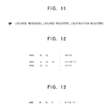
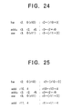
- the program when executing the program shown in Fig. 24 for the conventional microprocessor, the program can be written as shown in Fig. 12.
- the instruction "mov r0, r2" indicates to transfer data of the internal memory 47 stored in the data register r0 to the register r2.
- the instruction "add r2, r9, r3" indicates to add the data stored in the register r2 and the data stored in the register r9 and store the result to the register r3.
- the data stored in the register r2 is output to the port AIN of the ALU 13
- the data stored in the register r9 is output to the port BIN
- the ALU 13 adds the same.
- the result of the addition is written from the port AOUT through the bus 23 into the register r3 in the general-purpose register module 11.
- the instruction "mov r3, r1" indicates to transfer the data stored in the register r3 to the data register r1.
- the data stored in the register r3 is transferred to the register r1 through for example the bus 17, multiplexer 12, bus 23, multiplexer 16, and bus 25. After this, the data stored in the data register r1 is automatically written by the hardware via the bus 27 to the address, of the internal memory 47, stored in the DP register 31.
- the program shown in Fig. 12 can be written, for example, as shown in Fig. 13.
- the data registers r0 and r9 are designated as the source registers of the instruction "add”, and the data register r1 is designated as a destination address.
- the program shown in Fig. 13 is executed by the microprocessor 1 in one clock cycle.
- the addresses stored in the DP registers 30 and 31 shown in Fig. 2 are successively updated by for example adding "+4" so as to successively access the addresses at "+4" intervals in the internal memory 47 via the data registers r0 and r1.
- the instruction "add r0, r9, r1" indicates to add the data stored in the data register r0 and the data stored in the register r9 and store the result of the addition in the data register r1.
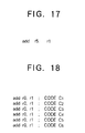
- the microprocessor 1 for example, by treating the register r14 in the general-purpose register module 11 shown in Fig. 3 as a data register and further providing a DP register corresponding to the register r14, it is possible to establish three systems of paths for the memory access. In this case, by writing a program as shown in Fig. 15, it is possible to designate the data registers r0, r14, and r1 in all of the three operands of the addition instruction "add".
- the access to the internal memory 47 is treated as an extension of the access to the general-purpose registers, and the data registers r0 and r1 can be used as memory windows by software.
- the microprocessor 1 when the addresses in the internal memory 47 to be accessed and the order of accessing are predetermined, by using the address updating function of the DP registers 30 and 31 to automatically update the addresses stored in the DP registers 30 and 31, it is not necessary to write the procedure for the memory access in the program distinctly every time.
- microprocessor 1 by providing two DP (data pointer) registers 30 and 31 and executing the ALU processing instructions directly on the data in the internal memory 47, for example, it is possible to write the processing for reading and processing the data on the internal memory 47, then write it back to the internal memory 47 in one instruction.
- DP data pointer
- both of the DP registers 30 and 31 are capable of designating all of the addresses in the internal memory 47, if the address of data to be read from the internal memory 47 and the address of the data to be written in the internal memory 47 are different, the instruction can be executed within one clock cycle.
- microprocessor 1 when repeatedly (consecutively) executing an instruction to write back data to the internal memory 47 (data transfer instruction designating the data register r0 or r1 as a destination register), it is possible to stop the automatic read function of the DP registers 30 and 31 to eliminate wasteful memory read operations. As a result, it is possible to consecutively execute memory write operations and realize multiplexing of instructions.
- the MEM stage in the conventional five-stage pipeline processing shown in Fig. 23 becomes unnecessary and the four-stage pipeline configuration as shown in Fig. 4 can be applied.
- the read operation to the internal memory 47 is carried out using the data registers r0 and r1
- the write operation to the internal memory 47 can be performed by the register write operation performed at the WB stage. Therefore, it is not necessary to separately provide the stage for memory access processing in the pipeline processing.
- the control circuit of the processor as a whole can be simplified, and it is possible to flexibly deal with exceptional processing including external interruption processing.
- the microprocessor 81 of the present embodiment has basically the same configuration as the microprocessor 1 of the above-mentioned microprocessor 1 except for the number of the banks in the internal memory, the numbers of data registers and DP registers, and the provision of a multiplexer 82 in place of the multiplexers 12 and 16 shown in Fig. 1.
- Figure 16 is a view of the configuration around the internal memory 87 of the microprocessor 81 of the present embodiment.
- the microprocessor 1 comprises an internal memory 87, DP registers 91, 92, and 93, data registers r0, r1-R, and r1-W, a multiplexer 82, and buses 101 to 106.
- microprocessor 81 in the same way as the microprocessor 1 shown in Fig. 1, comprises the ALU 13, program counter 34, instruction page memory 35, decoder 36, and buses 17, 18, 19, 20, and 23.
- the microprocessor 81 uses the register r1 shown in Fig. 1 as the register r1-R and uses the register r2 as the register r1-W. Namely, the microprocessor 81 comprises the registers r2 to r15 in addition to the registers r0, r1-R, and r1-W.
- the physical data register r1-R and data register r1-W are treated as one data register r1 logically in writing a program.
- the microprocessor 81 reads data from an address, of the memory bank 110 in the internal memory 47, stored in the DP register, and stores it in the data register r0.
- the data register r1-R is exclusively for read operations of the data from the memory bank 111 of the internal memory 87.
- the address of the logical data register r1 serving as a destination register is designated in the two-operand processing instruction written in the program, it stores the data read from the address, of the memory bank 111, stored in the DP register 92.
- the data register r1-W is exclusively for write operations of data to the memory bank 112 of the internal memory 87.
- an address of the logical data register r1 serving as a destination register is designated in the two-operand processing instruction written in the program, it writes the data stored in the data register r1-W to the address, of the memory bank 112, stored in the DP register 93.
- the address of the logical data register r1 can be indirectly designated, for example, by a logical address via a logical register name, other than being designated directly by a logical address.
- the microprocessor 81 executes a two-operand processing instruction having, for example, the format shown in Fig. 6.
- the microprocessor 81 When the microprocessor 81, for example, as shown in Fig. 17, executes an instruction which designates the data register r1 as a destination address, it first writes to the DP register 92 the address of the memory bank 111 at which the data to be added is stored, then reads, to the data register r1-R via the bus 102, the data to be added.
- the ALU 13 shown in Fig. 1 performs the processing for adding the data stored in the register r5 and the data stored in the data register r1-R and stores the result in the data register r1-W via the bus 106. Further, it writes in the DP register 93 the address of the memory bank 112 to which the data of the result of addition is written back.
- the data of the result of addition stored in the data register r1-W is written back to the memory bank 112 via the bus 103, by hardware.
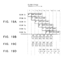
- microprocessor 81 When the microprocessor 81, for example, executes the program shown in Fig. 18 by the four-stage pipeline processing shown in Fig. 4, the processing becomes as shown in Fig. 19(A).
- the instruction "add r0, r1" is fetched at the IF stage, one of the data to be added which is read from the address, of the memory bank 110, stored in the DP register 91, to the data register r0, is output from the data register r0 to the port AIN of the ALU 13 at the DEC stage.
- the other data to be added which is read from the address, of the memory bank 111, stored in the DP register 92, to the data register r1-R, is output from the data register r1-R to the port BIN of the ALU 13.
- the IF stage of the code C1 is performed at the clock cycle T.
- the memory read operations (decode stage) to the data register r0 by the codes C1 to C6 are carried out in turn at the clock cycles T+1 to T+6.
- the memory read operations (decode stage) to the data register r1-R by the codes C1 to C6 are carried out in turn at the clock cycles T+1 to T+6.
- the memory write operations (WB stage) to the data register r1-W by the codes C1 to C6 are carried out in turn at the clock cycles T+3 to T+8.
- the microprocessor 81 by providing the data registers r1-R and r1-W, it is possible to perform the memory read operation and the memory write operation to the data register r1 simultaneously. As a result, the codes C1 to C6 shown in Fig. 18 can be executed within one clock cycle.
- microprocessor 81 it is possible to access three different bits of data in the internal memory 87 in the same clock cycle, using a two-operand processing instruction, and to realise processing substantially similar to three-operand processing.
- the present invention is not limited to the above embodiments.
- the example was given of the case of using two general-purpose registers as the data registers r0 and r1 in the general-purpose register module 11, but any number of registers can be used so long as it is one or more.
- the data registers r0 and r1 can be used as first-in-first-out (FIFO) memories for communication between microprocessors in a parallel processing processor having a plurality of microprocessors.
- the data registers r0 and r1 can be used as local memories or stack memories.
- the multiplexers 12 and 16 are provided independently, however, the function of the multiplexer 16 can be included in the multiplexer 12.
- the internal memory was configured separated into two banks, however, the internal memory may also be configured separated into three or more banks or configured without being separated into banks.
- the data registers r0 and r1 are provided as part of the plurality of general-purpose registers in the general-purpose register module 11, however, the data registers r0 and r1 can be provided outside the general-purpose register module 11 and treated as separate from the general-purpose registers.
- microprocessor 81 having the memory configuration shown in Fig. 16, it is also possible to provide three FIFO memories instead of the internal memory 87, connecting the input use FIFO memory to the data register r1-R, and connecting the output use FIFO memory to the data register r1-W.
- microprocessor of the present invention by using the general-purpose registers as data pointer registers, it is possible to treat access to the internal memory in the same way as access to the general-purpose registers.
- the microprocessor of the present invention since the write operation to the internal memory is performed using a second data register, it is possible to perform the write operation to the internal memory by a register write operation performed in the write back operation. As a result, there is no need to separately provide a memory access stage in the pipeline processing and it is possible to perform four-stage pipeline processing. As a result, effective processing can be realised by a simple hardware configuration.
- the read operation and write operation of data between a first data register, second data register, and internal memory can be performed in parallel with the pipeline processing, thus the pipeline processing can be performed smoothly without stalling and a high processing capability can be brought out.
Applications Claiming Priority (2)
| Application Number | Priority Date | Filing Date | Title |
|---|---|---|---|
| JP9216827A JPH1165840A (ja) | 1997-08-11 | 1997-08-11 | 演算処理装置およびその方法 |
| JP216827/97 | 1997-08-11 |
Publications (1)
| Publication Number | Publication Date |
|---|---|
| EP0897146A2 true EP0897146A2 (fr) | 1999-02-17 |
Family
ID=16694525
Family Applications (1)
| Application Number | Title | Priority Date | Filing Date |
|---|---|---|---|
| EP98402033A Withdrawn EP0897146A2 (fr) | 1997-08-11 | 1998-08-11 | Appareil de traitement arithmétique et procédé du même |
Country Status (3)
| Country | Link |
|---|---|
| US (1) | US6725355B1 (fr) |
| EP (1) | EP0897146A2 (fr) |
| JP (1) | JPH1165840A (fr) |
Cited By (1)
| Publication number | Priority date | Publication date | Assignee | Title |
|---|---|---|---|---|
| EP0969357A2 (fr) * | 1998-06-30 | 2000-01-05 | Sun Microsystems, Inc. | Exécution d'instructions avec un compteur de programme et un ou plusieurs compteurs de données |
Families Citing this family (7)
| Publication number | Priority date | Publication date | Assignee | Title |
|---|---|---|---|---|
| US7587582B1 (en) * | 1998-12-03 | 2009-09-08 | Sun Microsystems, Inc. | Method and apparatus for parallel arithmetic operations |
| AU2597401A (en) * | 1999-12-22 | 2001-07-03 | Ubicom, Inc. | System and method for instruction level multithreading in an embedded processor using zero-time context switching |
| US7047396B1 (en) * | 2000-06-22 | 2006-05-16 | Ubicom, Inc. | Fixed length memory to memory arithmetic and architecture for a communications embedded processor system |
| US7822950B1 (en) | 2003-01-22 | 2010-10-26 | Ubicom, Inc. | Thread cancellation and recirculation in a computer processor for avoiding pipeline stalls |
| US7680990B2 (en) * | 2003-05-30 | 2010-03-16 | Hewlett-Packard Development Company, L.P. | Superword memory-access instructions for data processor |
| JP2008129667A (ja) * | 2006-11-17 | 2008-06-05 | Meidensha Corp | プログラマブルコントローラ |
| KR102534825B1 (ko) * | 2016-04-19 | 2023-05-22 | 에스케이하이닉스 주식회사 | 메모리 제어장치 및 이를 포함하는 데이터 저장 장치 |
Family Cites Families (12)
| Publication number | Priority date | Publication date | Assignee | Title |
|---|---|---|---|---|
| US4777587A (en) * | 1985-08-30 | 1988-10-11 | Advanced Micro Devices, Inc. | System for processing single-cycle branch instruction in a pipeline having relative, absolute, indirect and trap addresses |
| DE3782819D1 (de) * | 1987-06-02 | 1993-01-07 | Itt Ind Gmbh Deutsche | Steuerprozessor. |
| US5187799A (en) * | 1988-05-17 | 1993-02-16 | Calif. Institute Of Technology | Arithmetic-stack processor which precalculates external stack address before needed by CPU for building high level language executing computers |
| JPH04275628A (ja) * | 1991-03-01 | 1992-10-01 | Mitsubishi Electric Corp | 演算処理装置 |
| JP2665081B2 (ja) * | 1991-07-08 | 1997-10-22 | 三菱電機株式会社 | マイクロコンピュータのレジスタ間データ転送方式 |
| US5685005A (en) * | 1994-10-04 | 1997-11-04 | Analog Devices, Inc. | Digital signal processor configured for multiprocessing |
| US5619720A (en) * | 1994-10-04 | 1997-04-08 | Analog Devices, Inc. | Digital signal processor having link ports for point-to-point communication |
| US5692207A (en) * | 1994-12-14 | 1997-11-25 | International Business Machines Corporation | Digital signal processing system with dual memory structures for performing simplex operations in parallel |
| US6029242A (en) * | 1995-08-16 | 2000-02-22 | Sharp Electronics Corporation | Data processing system using a shared register bank and a plurality of processors |
| JP3510729B2 (ja) * | 1996-02-29 | 2004-03-29 | 三洋電機株式会社 | 命令実行方法および命令実行装置 |
| US5854939A (en) * | 1996-11-07 | 1998-12-29 | Atmel Corporation | Eight-bit microcontroller having a risc architecture |
| US6425070B1 (en) * | 1998-03-18 | 2002-07-23 | Qualcomm, Inc. | Variable length instruction decoder |
-
1997
- 1997-08-11 JP JP9216827A patent/JPH1165840A/ja active Pending
-
1998
- 1998-08-11 EP EP98402033A patent/EP0897146A2/fr not_active Withdrawn
- 1998-08-11 US US09/132,413 patent/US6725355B1/en not_active Expired - Fee Related
Cited By (3)
| Publication number | Priority date | Publication date | Assignee | Title |
|---|---|---|---|---|
| EP0969357A2 (fr) * | 1998-06-30 | 2000-01-05 | Sun Microsystems, Inc. | Exécution d'instructions avec un compteur de programme et un ou plusieurs compteurs de données |
| EP0969357A3 (fr) * | 1998-06-30 | 2000-09-13 | Sun Microsystems, Inc. | Exécution d'instructions avec un compteur de programme et un ou plusieurs compteurs de données |
| US6467037B1 (en) | 1998-06-30 | 2002-10-15 | Sun Microsystems, Inc. | Utilizing a program counter with one or more data counters for executing instructions |
Also Published As
| Publication number | Publication date |
|---|---|
| US6725355B1 (en) | 2004-04-20 |
| JPH1165840A (ja) | 1999-03-09 |
Similar Documents
| Publication | Publication Date | Title |
|---|---|---|
| US5706490A (en) | Method of processing conditional branch instructions in scalar/vector processor | |
| US7020763B2 (en) | Computer processing architecture having a scalable number of processing paths and pipelines | |
| US6434689B2 (en) | Data processing unit with interface for sharing registers by a processor and a coprocessor | |
| US5067069A (en) | Control of multiple functional units with parallel operation in a microcoded execution unit | |
| US6058465A (en) | Single-instruction-multiple-data processing in a multimedia signal processor | |
| US5881307A (en) | Deferred store data read with simple anti-dependency pipeline inter-lock control in superscalar processor | |
| JP3864160B2 (ja) | 複数型レジスタ・セットを採用したriscマイクロプロセッサ・アーキテクチャ | |
| US5185872A (en) | System for executing different cycle instructions by selectively bypassing scoreboard register and canceling the execution of conditionally issued instruction if needed resources are busy | |
| EP2176741A1 (fr) | Procédé et système d'expansion d'une instruction conditionnelle en une instruction inconditionnelle et une instruction de sélection | |
| US5544337A (en) | Vector processor having registers for control by vector resisters | |
| US7139899B2 (en) | Selected register decode values for pipeline stage register addressing | |
| EP1446717A1 (fr) | Procede et dispositif d'interfa age d'un processeur et d'un coprocesseur | |
| US5623650A (en) | Method of processing a sequence of conditional vector IF statements | |
| US6035388A (en) | Method and apparatus for dual issue of program instructions to symmetric multifunctional execution units | |
| US6725355B1 (en) | Arithmetic processing architecture having a portion of general-purpose registers directly coupled to a plurality of memory banks | |
| JP3790626B2 (ja) | デュアルワードまたは複数命令をフェッチしかつ発行する方法および装置 | |
| US7237088B2 (en) | Methods and apparatus for providing context switching between software tasks with reconfigurable control | |
| US6704857B2 (en) | Methods and apparatus for loading a very long instruction word memory | |
| US7024540B2 (en) | Methods and apparatus for establishing port priority functions in a VLIW processor | |
| US5598547A (en) | Vector processor having functional unit paths of differing pipeline lengths | |
| US7080234B2 (en) | VLIW computer processing architecture having the problem counter stored in a register file register | |
| US20020087821A1 (en) | VLIW computer processing architecture with on-chip DRAM usable as physical memory or cache memory | |
| EP1050800A1 (fr) | Unité d'exécution en pipeline | |
| JPH02211534A (ja) | 並列処理装置 | |
| JPH1165841A (ja) | 演算処理装置およびその方法 |
Legal Events
| Date | Code | Title | Description |
|---|---|---|---|
| PUAI | Public reference made under article 153(3) epc to a published international application that has entered the european phase |
Free format text: ORIGINAL CODE: 0009012 |
|
| AK | Designated contracting states |
Kind code of ref document: A2 Designated state(s): AT BE CH CY DE DK ES FI FR GB GR IE IT LI LU MC NL PT SE |
|
| AX | Request for extension of the european patent |
Free format text: AL;LT;LV;MK;RO;SI |
|
| STAA | Information on the status of an ep patent application or granted ep patent |
Free format text: STATUS: THE APPLICATION IS DEEMED TO BE WITHDRAWN |
|
| 18D | Application deemed to be withdrawn |
Effective date: 20030301 |